EP0285661A1 - Lagedetektor des optischen brennpunktes eines optischen daten-speicher-/lesegerätes - Google Patents
Lagedetektor des optischen brennpunktes eines optischen daten-speicher-/lesegerätes Download PDFInfo
- Publication number
- EP0285661A1 EP0285661A1 EP87905647A EP87905647A EP0285661A1 EP 0285661 A1 EP0285661 A1 EP 0285661A1 EP 87905647 A EP87905647 A EP 87905647A EP 87905647 A EP87905647 A EP 87905647A EP 0285661 A1 EP0285661 A1 EP 0285661A1
- Authority
- EP
- European Patent Office
- Prior art keywords
- light
- information recording
- recording medium
- optical sensor
- spot position
- Prior art date
- Legal status (The legal status is an assumption and is not a legal conclusion. Google has not performed a legal analysis and makes no representation as to the accuracy of the status listed.)
- Granted
Links
Images







Classifications
-
- G—PHYSICS
- G11—INFORMATION STORAGE
- G11B—INFORMATION STORAGE BASED ON RELATIVE MOVEMENT BETWEEN RECORD CARRIER AND TRANSDUCER
- G11B7/00—Recording or reproducing by optical means, e.g. recording using a thermal beam of optical radiation by modifying optical properties or the physical structure, reproducing using an optical beam at lower power by sensing optical properties; Record carriers therefor
- G11B7/12—Heads, e.g. forming of the optical beam spot or modulation of the optical beam
- G11B7/125—Optical beam sources therefor, e.g. laser control circuitry specially adapted for optical storage devices; Modulators, e.g. means for controlling the size or intensity of optical spots or optical traces
-
- G—PHYSICS
- G11—INFORMATION STORAGE
- G11B—INFORMATION STORAGE BASED ON RELATIVE MOVEMENT BETWEEN RECORD CARRIER AND TRANSDUCER
- G11B7/00—Recording or reproducing by optical means, e.g. recording using a thermal beam of optical radiation by modifying optical properties or the physical structure, reproducing using an optical beam at lower power by sensing optical properties; Record carriers therefor
- G11B7/08—Disposition or mounting of heads or light sources relatively to record carriers
- G11B7/09—Disposition or mounting of heads or light sources relatively to record carriers with provision for moving the light beam or focus plane for the purpose of maintaining alignment of the light beam relative to the record carrier during transducing operation, e.g. to compensate for surface irregularities of the latter or for track following
-
- G—PHYSICS
- G11—INFORMATION STORAGE
- G11B—INFORMATION STORAGE BASED ON RELATIVE MOVEMENT BETWEEN RECORD CARRIER AND TRANSDUCER
- G11B7/00—Recording or reproducing by optical means, e.g. recording using a thermal beam of optical radiation by modifying optical properties or the physical structure, reproducing using an optical beam at lower power by sensing optical properties; Record carriers therefor
- G11B7/08—Disposition or mounting of heads or light sources relatively to record carriers
- G11B7/09—Disposition or mounting of heads or light sources relatively to record carriers with provision for moving the light beam or focus plane for the purpose of maintaining alignment of the light beam relative to the record carrier during transducing operation, e.g. to compensate for surface irregularities of the latter or for track following
- G11B7/0908—Disposition or mounting of heads or light sources relatively to record carriers with provision for moving the light beam or focus plane for the purpose of maintaining alignment of the light beam relative to the record carrier during transducing operation, e.g. to compensate for surface irregularities of the latter or for track following for focusing only
-
- G—PHYSICS
- G11—INFORMATION STORAGE
- G11B—INFORMATION STORAGE BASED ON RELATIVE MOVEMENT BETWEEN RECORD CARRIER AND TRANSDUCER
- G11B7/00—Recording or reproducing by optical means, e.g. recording using a thermal beam of optical radiation by modifying optical properties or the physical structure, reproducing using an optical beam at lower power by sensing optical properties; Record carriers therefor
- G11B7/08—Disposition or mounting of heads or light sources relatively to record carriers
- G11B7/09—Disposition or mounting of heads or light sources relatively to record carriers with provision for moving the light beam or focus plane for the purpose of maintaining alignment of the light beam relative to the record carrier during transducing operation, e.g. to compensate for surface irregularities of the latter or for track following
- G11B7/0908—Disposition or mounting of heads or light sources relatively to record carriers with provision for moving the light beam or focus plane for the purpose of maintaining alignment of the light beam relative to the record carrier during transducing operation, e.g. to compensate for surface irregularities of the latter or for track following for focusing only
- G11B7/0917—Focus-error methods other than those covered by G11B7/0909 - G11B7/0916
-
- G—PHYSICS
- G11—INFORMATION STORAGE
- G11B—INFORMATION STORAGE BASED ON RELATIVE MOVEMENT BETWEEN RECORD CARRIER AND TRANSDUCER
- G11B7/00—Recording or reproducing by optical means, e.g. recording using a thermal beam of optical radiation by modifying optical properties or the physical structure, reproducing using an optical beam at lower power by sensing optical properties; Record carriers therefor
- G11B7/12—Heads, e.g. forming of the optical beam spot or modulation of the optical beam
Definitions
- the present invention relates to a focus spot detection device of an optical information recording and reproducing device in which an information is recorded in and reproduced from an information recording medium and erased by means of light beam and, particularly, to a focusing error and tracking error detection device.
- Figs. 10 and 11 show an example of a focusing error detection device for an optical head such as shown in Japanese Patent Application Laid-open No. 93223/1977 or J.M. Breat and G. Bouwhuis, "Position Sensing In Videodisc Read Out", Applied Optics, vol.17, No.13, p.p. 2013 - 2021, (1978).
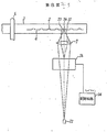
- FIG. 10 1 depicts a light source such as a HeNe laser and 2 is an auxiliary lens for expanding a diameter of light beam emitted by the light source 1.
- 3 depicts an information recording medium such as an optical disk, 4 an information recording plane of the information recording medium 3 and 5 an information track, the information recording medium 3 being rotatable around a rotary shaft 6.
- 7 depicts a half mirror for separating irradiation light to the information recording medium 3 from reflection light from the information recording medium 3, 8 a mirror for bending an optical path of the irradiation light to the information recording medium 3 and 9 an objective lens for focusing the irradiation light from the light source 1 onto the information track 5.
- FIG. 10 depicts a focusing error detection sensor which is composed of a plurality of optical detecting elements.
- 11 depicts an auxiliary lens for projecting an image formed on an exit pupil of the objective lens 9 by a reflection light from the information recording medium 3 onto the optical detecting elements in the focusing error detecting sensor 10.
- an image of a point a on the exit pulpil of the objective lens 9 is formed on the focusing error detecting sensor 10 as a point a' by the auxiliary lens 11.
- FIG. 11 depict the optical detecting elements in the focusing error detecting sensor
- 14 a subtractor for providing a difference between output signals from the optical detecting elements 12 and 13,
- an adder for adding the output signals of the detecting elements 12 and 13,
- 16 a phase shifter for shifting a phase of an output signal of the adder 15 by 90°
- 17 a multiplier for multiplying an output of the phase shifter 16 with the output signal of the subtractor 14 and 18 a low pass filter for passing a low frequency component of the output signal of the multiplier.
- This focusing error detecting device is based on the fact that, in reading an information on the information recording plane 4 which acts as a diffraction grating, there is produced a phase difference between 0 order light directly reflected by the information recording medium and the first order diffraction light reflected and diffracted by information pits on an information track thereof and the phase difference corresponds to a focusing error.
- the phase difference between the 0 order light and the first order diffraction light can be measured by analysing interference fringes in an interference region of the 0 order light and the first order diffraction light in a plane remote enough from the information recording medium, that is, a plane in which the 0 order light and the first order diffraction light can be observed with an enough distance therebetween (the latter plane will be referred to hereinafter as a plane disposed in a " remote region" of the information recording medium ) and, in the conventional device, a focusing error signal is produced by electrically processing outputs of a plurality of optical detecting elements arranged in the remote region.
- E and ⁇ axes are set on the information recording plane 4 of the information recording medium 3 in parallel with a center line of the information track 5 and orthogonally of the center line, respectively.
- the exit pupil plane of the objective lens 9 which focuses light beam onto the information recording medium 3 is referred to as XY plane, with an origin of the XY plane being made coincident with a center of the exit pupil plane and an X axis being made in parallel with then axis.
- An entrance pupil plane of the objective lens 9 in which reflection light is fallen is set as an X'Y' plane which is the same plane as the XY plane.
- Fig. 12 shows a correspondency of the above mentioned coordinate system.
- an information recording plane of an optical video disc or compact disc it is found that a plurality of information tracks are arranged on the plane equidistantly (1.6 - 1.7 ⁇ m gap).
- This means that such disc is.a diffraction grating having a single spatial frequency with respect to a direction orthogonal to the information tracks.
- a direction parallel with the information tracks an information is recorded by changing pit position, pit period and pit length etc. Therefore, spatial frequency spectrum in a direction parallel with the information tracks is not single but broadened considerably.
- Fig. 13 21 depicts information pit which, in the case of the optical video disc, is a land or recess having a physical depth in the order of 0.1 ⁇ m compared with a peripheral portion thereof. Representing a period in the track direction axis) of the information recording plane and a period in the direction-( n axis direction) perpendicular to the information track by P and Q, respectively, periods p and q for the normalized coordinates u and v shown in Fig.
- u 0 is an amount of movement of the information recording medium in the track direction in the normalized coordinates
- v o is a deviation of track in the direction perpendicular to the track
- a(x,y) is irradiation light amplitude distribution on the exit pupil of the objective lens, i.e., pupil function.
- a wavefront aberration coefficient W 20 of off-focusing corresponding to te off-focus ⁇ f is given by (cf. G.Bouwhis et al, "Principals of Optical Disc Systems", Adam Hilger,.p. 41,(1985)). Therefore, when it is assumed that an optical system from the light source 1 to the information recording plane 4 is aberration free, the irradiation light amplitude distribution a(x,y) on the objective lens can be represented bv
- the optical detecting elements 12 and 13 have rectangular light receiving surfaces such as shown in Fig. 11 or 15, respectively, the longitudinal direction thereof being transversal to the information track 5, i.e., in parallel with the y' axis. Further, since the elements 12 and 13 are arranged in an interference region of (0,0) order reflection light and (1,0) order reflection and diffraction light, the amplitude distribution A D1 (x',y') of reflection light from the information recording medium 3 on the optical sensor can be represented by using the equation (8) as follows: In this expression, (m,n) order diffraction light means, among light components of light reflected and diffracted by the information recording medium acting as the two dimensional diffraction grating, diffraction light having diffraction order of m order in the track direction and n order in the direction perpendicular thereto.
- a D1 (x' ,Y') can be written as When it is assumed that the amplitude distribution of irradiation light on the exit pupil of the objective lens is constant and A D1 (x',y') can be represented by using the equation 10 in the equation 13 as follow. Since, when the information recording medium 3 is rotating around the rotary shaft 6 at a line speed So in the normalized coordinate u, the following equation is established the equation 16 can be rewritten as follow: The meaning of the equation 18 is as follow:
- interference fringes observed on the optical sensor surface can be said as a progrresive wave propagating along the x' axis, which has a period varying depending upon an amount of W 20' i.e., off-focusing ⁇ f and a traveling direction depending upon a sign of W 20 .
- a difference signal I DF and a sum signal I SUM of the elements 12 and 13, which are derived from the subtractor 14 and the adder 15, respectively, are written as follows: Since, when the off-focusing is not considerably large, the following equation is established the equations 20 and 21 can be simplified as follows, respectively: Then, the output I SUM of the adder is supplied to the phase . shifter 16 to obtain a signal I R the phase of a.c.
- a focusing error signal Sf is obtained by passing the Signal S M through the low pass filter 18 capable of passing signal component whose angular frequency is smaller than 2w , which is as follow: Since the signal Sf is an odd function of the wavefront aberration coefficient W 20' i.e., the amount of off-focusing ⁇ f, it can be used to correct the focusing according to the known method.
- the focusing error signal is produced by a synchronous detection of the difference signal from the two optical detecting elements with using the sum signal thereof as a reference signal. Therefore, both of the difference signal and the sum signal must be single frequency signals variable with time. This means that it requires, in the information recording medium, a constant spatial frequency ina direction parallel with the information track. Therefore, since it is impossible for some information recording medium such as the compact disc in which information is recorded by modulating it to the pit length and the pit gap to derive single frequency signal to be used as the reference signal, it is impossible to produce the focusing error signal.
- the present invention was made in view of elimination of such problems as above and an object thereof is to provide a focusing error detection device capable of producing a focusing error signal even for an information recording medium having no periodicity in a direction parallel with information tracks thereof. Another object of the present invention is to provide a focusing error detection device which requires substantially no additional optical element ( cylindrical lens, prism etc.) which is the feature of the conventional device for production of such focusing error signal and in which a positional regulation of an optical sensor for focusing error detection is much facilitated.
- a focusing error detection device produces a focusing error signal by arranging an optical sensor for focusing error detection which composed of a plurality of optical detecting elements in a remote region of an information recording medium, providing a plurality of light sources for producing a plurality of condensed light spots in a direction perpendicular to information tracks thereof and processing interference fringes produced in the remote region of the information recording medium by these light sources by using the optical sensor and an operation circuit and a control circuit which are connected to an output of the optical sensor.
- the plurality of light sources juxtaposed vertically with respect to the information tracks produce interference fringes having constant phase relation to each other in the remote region of the information recording medium.
- the focusing error detection sensor having the optical elements arranged in a direction parallel with in an interference region of 0 order light reflected from the information recording medium and 1 order light reflected and diffracted by the information track detects interference fringes produced due to diffraction phenomenon by the information tracks. Further, the light sources and the operation circuit which operate in synchronism with each other analyse the interference finges to produce the focusing error signal.
- the focusing error signal is produced by scanning vertically with respect to the information track the condensed light spots on the information recording medium produced by using the plurality of light sources and analysing interference fringes resulting from diffraction by the information track by means of the optical sensor disposed in the remote region of the medium and the electronic circuits connected thereto, it is possible to produce the focusing error stably even if the information recording medium is that having spreaded pit length and/or pit distance or that having a continuous guide groove. Further, it is possible to provide a condensed light spot position-detecting device whose optical system is simplified and positional regulation of the optical sensor is much facilitated.
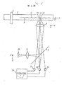
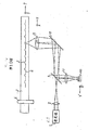
- Fig. 1 shows a construction of an optical system according to an embodiment of the present invention
- Fig. 2 shows an optical sensor and an electronic circuit for detecting a focusing error according to an embodiment of the present invention
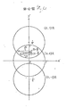
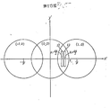
- Fig. 3 shows a coordinate system and a lateral movement of condensed light spot for explanation of the principle of the present invention
- Fig. 4 shows a positional relaion between a reflection light from an information recording medium and the optical sensor
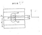
- Fig. 5 shows positions of the condensed light spots on the information recording medium
- Figs. 6 and 7 show an optical sensor and an electronic circuit necessaryto detect a tracking error
- Fig. 8 shows an optical system when an acoustooptical modulator is used as a condensed light spot scanner
- Fig. 1 shows a construction of an optical system according to an embodiment of the present invention
- Fig. 2 shows an optical sensor and an electronic circuit for detecting a focusing error according to an embodiment of the present invention
- Fig. 3 shows a coordinate system and a
- FIG. 9 shows an optical system when a diffraction gratings and wavelength variable light sources are used as the condensed light spot scanner
- Figs. 10 and 11 show a construction of a conventional focusing error detection device
- Fig. 12 shows a coordinate system useful to explan the principle of focusing error detection
- Fig. 13 shows information pits on the information recording medium
- Fig. 14 illustrates off-focusing state
- Fig. 15 shows a positional relation between reflection light from information recording medium and an optical sensor in the conventional device.
- FIGs. 1 and 2 which show a construction of an embodiment of the present invention, reference numerals 3 to 7 10 and 11 depict the same components as those of the conventional device.
- 21, 22 and 23 depict light sources such as semiconductor lasers, 24 a cntrol circuit for on-off controlling the light sources 21, 22 and 23, 25, 26 and 27 spots of lights emitted from the light sources 21, 22 and 23, respectively, and 28 an optical sensor composed of a plurality of sensor elements for focusing error detection.
- Fig. 2 29, 30, 31 and 32 depict the sensor elements of the optical sensor 28, 33 a subtractor, 34 an adder, 35 to 40 sample-hold circuits, 41 and 42 adders, 43 and 44 subtractors and 47 an adder. Reading of data by the sample-hold circuits 35 to 40 is performed in synchronism with the on-off operation of the light sources 21 to 23.
- the principle of focusing error detection of the present device is based on the fact that, when an information is read in or out from an information recording surface acting as diffraction grating as in the conventional device, there is a phase difference produced between 0 order light directly reflected by the information recording medium and ⁇ 1 order light reflected and diffracted by information tracks, which corresponds to a focusing error.
- the phase difference between ⁇ 1 order light reflected and diffracted by the row of pits and 0 order light a phase difference between 0 order light and ⁇ 1 order light reflected and diffracted by information tracks, in this embodiment. Therefore, although, in the conventional device, the row of information pits must have single spatial frequencies t least partially, there is no such requirement in this embodiment since the phase difference between 0 order light and 1 order light is detected by scanning the light spots on the information recording medium vertically with respect to the information tracks.
- an amplitude distribution a(x,y) of irradiation light on the exit pupil plane of the objective lens can be expressed as follows: Then, the amplitude distribution A D0,1 (x' ,y') of reflection light on optical elements 30 and 31 arranged in an interference region of the (0,0) order reflection light and the (0,1) order reflection and diffraction light as shown in Fig. 4 will be considered.
- the output currents I D1 and I D2 of the optical sensor elements 30 and 31 arranged along the x' direction are given as follows: where (y - ⁇ /2) and (y + ⁇ /2) are center positions of the optical sensor elements having the same light receiving areas and widths in the y' direction small enough compared with lengths in the x' direction, the width being small enough compared with the period of the interference fringes, and K 1 is a constant proportional to the sensitivity of the optical sensor and the light receiving area thereof.
- the method of obtaining the focusing error signal by varying in step the aberration coefficient W 11 of lateral image movement of light irradiation to the information recording medium i.e., by shifting the light spot on the information recording plane in a direction traversing the information tracks ) to scan the interference fringes produced in the interference region of the (0,0) order light and the (0, 1) order light will be described.
- the present device performs the following operation.
- the light source 22 is energized and a light spot is moved to a position 26.
- the spot position may differ from that in F ig. 1, needless to say.
- the differential output and the sum output of the optical sensor elements are I DF (0) and I SUM (0), respectively, at this state, which are supplie sample-hold circuits 36 and 39, respectively.
- the light source 22 is deenergized and instead thereof the light source 21 is energized to produce a light spot 25 whose position is deviated vertically upwardly from the spot position 26 by one fourth the track interval, as shown in Fig. 5.
- the differential output and the sum output of the optical sensor are I DF ( ⁇ /2) and I SUM ( ⁇ /2), respectively, which are supplied to the sample-hold circuits 37 and 40, respectively.
- the light source 21 is deenergized and the light source 23 is energized. In the latter case, Ip V (- ⁇ /2) and I SUM (- ⁇ /2) are obtained.
- ⁇ F and I SUM obtained by energizing the light sources 21, 22 and 23 sequentially are processed by an operation circuit arranged downstream of the sample-hold circuits according to the equation 55 and a focusing error signal Sf is obtained. Since the semicinductor lasers used for the light sources can be modulated at high speed, it is possible to obtain the focusing error signal which is not influenced by recording signals and stable, by on-off controlling the light sources at a frequency higher enough than a frequency band of the information signal recorded on the information recording medium.
- the present invention is described as the focuing error detection device, it is easy to apply to the present device the Radial Wobbling method which is known as the tracking error detection method (cf. G.Bouwhis et al, "Principles of Optical Disc Systems", Adam Hilger Ltd.,p.p. 73 to 75).
- Fig. 6 shows an optical sensor and an operation circuit which are necessary to detect the tracking error, as an example.
- 48 depicts the optical sensor having a light receiving region which is a peripheral region of optical sensor elements 30 and 31 for the focusing error detection and which is adapted to receive all of light component of reflection from the information recording medium 4 which passed through the objective lens 9 and reflected by the half mirror 7.
- 49 depicts an adder for summing signals from the optical sensor elements 30, 31 and the optical sensor 48, 50 a band pass filter, 51 a multiplier and 52 a low pass filter. An operation of this tracking error deyection circuit will be described.
- the light sources 21, 22 and 23 are energized sequentially repeatedly with a time interval of from 21 to 22 to 23 to 22 to 21 ( a period of 4 T ) so that a light spot on the information recording plane 4 scans the information tracks 5 traversely from 25 to 26 to 27 to 26 to 25.
- all of the component of the reflection from the information recording plane 4 which passed through the objecive lens 9 and reflected by the half mirror 7 is received by the optical sensor elements 30 and 31 and the optical sensor 48 and converted into electric signals.
- the frequency component from the band pass filter 50 is compared in phase with a reference signal having frequency f supplied from the control circuit 24 by the multiplier 51 and the tracking error signal St is obtained by removing a component of frequency 2f by the low pass filter 52.
- tracking error signal S t can be obtained by using a circuit shown in Fig. 7 which functions similarly to the twin spot method ( cf. G.Bouwhis et al, "Principals of Optical Disc Systems", Adam Hilger Ltd.,p.p. 71 -72).
- Fig. 7 53 depicts a sample-hold circuit for sampling anf holding an electric signal corresponding to a reflection light component from the information recording medium 3 when the light source 21 is energized and 54 a sample-hold circuit for sampling and holding the electric signal when the light source 23 is energized.
- the tracking error signal can be obtained by differentiating outputs of these sample-hold circuits 53 and 54 by means of a subtractor 55.
- three discrete semiconductor lasers are used as the light sources.
- a wavelength variable light source can be used, such scanning can be realized by using a diffraction grating having a large wavelength scattering as a deflection means and changing an oscillation wavelength of a light source 58, as shown in Fig. 9.
- a semiconductor laser is known whose output wavelength can be changed by an injection current ( cf. L . G oldberg et al, "Frequency Modulation Characteristics of Coupled Stripe Laser Diode Array", IEEE J.Quantum Electron., QE-22, pp. 513 - 516(1986)).
- the present invention can be applied to not only the focus spot position detector of the optical information recording and reproducing device sich as the optical disc device but also to an optial spot position detection for other optical recording medium or articles.
Landscapes
- Physics & Mathematics (AREA)
- Optics & Photonics (AREA)
- Optical Recording Or Reproduction (AREA)
- Automatic Focus Adjustment (AREA)
Applications Claiming Priority (2)
| Application Number | Priority Date | Filing Date | Title |
|---|---|---|---|
| JP204261/86 | 1986-08-29 | ||
| JP61204261A JPH0640392B2 (ja) | 1986-08-29 | 1986-08-29 | 光学式情報記録再生装置の集光スポツト位置検出装置 |
Publications (3)
| Publication Number | Publication Date |
|---|---|
| EP0285661A1 true EP0285661A1 (de) | 1988-10-12 |
| EP0285661A4 EP0285661A4 (de) | 1989-07-25 |
| EP0285661B1 EP0285661B1 (de) | 1993-02-24 |
Family
ID=16487533
Family Applications (1)
| Application Number | Title | Priority Date | Filing Date |
|---|---|---|---|
| EP87905647A Expired - Lifetime EP0285661B1 (de) | 1986-08-29 | 1987-08-26 | Lagedetektor des optischen brennpunktes eines optischen daten-speicher-/lesegerätes |
Country Status (5)
| Country | Link |
|---|---|
| US (2) | US4888757A (de) |
| EP (1) | EP0285661B1 (de) |
| JP (1) | JPH0640392B2 (de) |
| DE (1) | DE3784342T2 (de) |
| WO (1) | WO1988001784A1 (de) |
Cited By (1)
| Publication number | Priority date | Publication date | Assignee | Title |
|---|---|---|---|---|
| GB2355354A (en) * | 1999-08-03 | 2001-04-18 | Axon Instr Inc | Auto-focus method |
Families Citing this family (14)
| Publication number | Priority date | Publication date | Assignee | Title |
|---|---|---|---|---|
| JPH0640392B2 (ja) * | 1986-08-29 | 1994-05-25 | 三菱電機株式会社 | 光学式情報記録再生装置の集光スポツト位置検出装置 |
| DE3882918T2 (de) * | 1987-11-17 | 1994-01-20 | Matsushita Electric Ind Co Ltd | Fokusregelsystem für optische Scheibenvorrichtung mit lichtempfindlichen Elementen in der Fokusebene des Bildes der Informationsstruktur. |
| EP0674308B1 (de) * | 1989-02-13 | 1998-05-27 | Omron Corporation | Optisches Wiedergabegerät für eine Karte |
| JP2923331B2 (ja) * | 1990-06-12 | 1999-07-26 | オリンパス光学工業株式会社 | 光記録媒体及びその再生装置 |
| KR930009220B1 (ko) * | 1991-08-20 | 1993-09-24 | 주식회사 금성사 | 광학기기의 옵티컬 픽-업장치 |
| US5511052A (en) * | 1992-05-11 | 1996-04-23 | Eastman Kodak Company | Digital compensator for controlling a servo to correct the value of a given parameter of a system |
| JP3612385B2 (ja) * | 1995-07-07 | 2005-01-19 | 松下電器産業株式会社 | 光ディスク装置 |
| US7831518B2 (en) * | 2001-11-20 | 2010-11-09 | Psi Systems, Inc. | Systems and methods for detecting postage fraud using an indexed lookup procedure |
| US7225984B2 (en) * | 2003-02-20 | 2007-06-05 | Harris Rodney C | Systems and methods for providing multiple object planes in an optical image scanning environment |
| JP4846339B2 (ja) * | 2004-10-26 | 2011-12-28 | ダイセン・メンブレン・システムズ株式会社 | 散気装置および散気システム |
| JP4716805B2 (ja) * | 2005-06-23 | 2011-07-06 | 三菱電線工業株式会社 | 多孔膜材及び散気装置 |
| JP4704881B2 (ja) * | 2005-10-13 | 2011-06-22 | ダイセン・メンブレン・システムズ株式会社 | 散気装置 |
| JP4726253B2 (ja) * | 2006-03-30 | 2011-07-20 | パイオニア株式会社 | 光ピックアップ及び情報機器 |
| JP5207240B2 (ja) * | 2008-08-11 | 2013-06-12 | 学校法人金井学園 | 光記録再生媒体の焦点誤差検出方法、およびそれに用いる発光装置のビーム分割調節器 |
Family Cites Families (9)
| Publication number | Priority date | Publication date | Assignee | Title |
|---|---|---|---|---|
| NL177157C (nl) * | 1975-02-28 | 1985-08-01 | Philips Nv | Inrichting voor het uitlezen van een vlakke registratiedrager met een optisch uitleesbare informatiestruktuur. |
| NL8103117A (nl) * | 1981-06-29 | 1983-01-17 | Philips Nv | Inrichting voor het beschrijven en/of uitlezen van een registratiedrager. |
| US4464567A (en) * | 1981-06-30 | 1984-08-07 | Storage Technology Corporation | Photoelectric information and focus detector |
| JPS58208944A (ja) * | 1982-05-31 | 1983-12-05 | Sony Corp | 光学ヘツド制御信号発生装置 |
| US4805162A (en) * | 1982-11-01 | 1989-02-14 | Storage Technology Partners Ii | Fine and coarse servo system for access and tracking on an optical disk |
| DE3675609D1 (de) * | 1985-08-27 | 1990-12-20 | Siemens Ag | Positioniereinrichtung fuer einen optischen plattenspeicher. |
| JPH0640392B2 (ja) * | 1986-08-29 | 1994-05-25 | 三菱電機株式会社 | 光学式情報記録再生装置の集光スポツト位置検出装置 |
| JPH06102096B2 (ja) * | 1992-08-20 | 1994-12-14 | 邦雄 毒島 | 弾球遊技機 |
| JPH0773626B2 (ja) * | 1992-08-20 | 1995-08-09 | 邦雄 毒島 | 弾球遊技機 |
-
1986
- 1986-08-29 JP JP61204261A patent/JPH0640392B2/ja not_active Expired - Lifetime
-
1987
- 1987-08-26 EP EP87905647A patent/EP0285661B1/de not_active Expired - Lifetime
- 1987-08-26 DE DE8787905647T patent/DE3784342T2/de not_active Expired - Lifetime
- 1987-08-26 WO PCT/JP1987/000632 patent/WO1988001784A1/ja not_active Ceased
-
1988
- 1988-04-22 US US07/196,190 patent/US4888757A/en not_active Expired - Lifetime
-
1989
- 1989-12-04 US US07/445,298 patent/US4999826A/en not_active Expired - Lifetime
Cited By (1)
| Publication number | Priority date | Publication date | Assignee | Title |
|---|---|---|---|---|
| GB2355354A (en) * | 1999-08-03 | 2001-04-18 | Axon Instr Inc | Auto-focus method |
Also Published As
| Publication number | Publication date |
|---|---|
| DE3784342T2 (de) | 1993-08-12 |
| EP0285661B1 (de) | 1993-02-24 |
| JPS6358627A (ja) | 1988-03-14 |
| US4999826A (en) | 1991-03-12 |
| DE3784342D1 (de) | 1993-04-01 |
| EP0285661A4 (de) | 1989-07-25 |
| JPH0640392B2 (ja) | 1994-05-25 |
| US4888757A (en) | 1989-12-19 |
| WO1988001784A1 (fr) | 1988-03-10 |
Similar Documents
| Publication | Publication Date | Title |
|---|---|---|
| CA1084162A (en) | Record playback system | |
| JP3549301B2 (ja) | 光ヘッドのトラッキング誤差検出装置 | |
| EP0285661B1 (de) | Lagedetektor des optischen brennpunktes eines optischen daten-speicher-/lesegerätes | |
| EP0219170B1 (de) | Gerät zum Abspielen oder Aufnehmen einer spurweise angeordneten optisch lesbaren Informationsstruktur | |
| KR950010418B1 (ko) | 광기록재생장치 | |
| US4006293A (en) | Apparatus for reading a flat record carrier with an optically readable information structure | |
| EP0201603A1 (de) | Spurnachführungsfehlerdetektorsystem eines optischen kopfes | |
| JPS6297141A (ja) | 光学走査装置 | |
| US4695992A (en) | Optical information recording-reproducing apparatus in which the relative position of a primary beam and secondary beams on recording medium is varied during recording and reproduction of information | |
| US4525825A (en) | Method and apparatus for detecting focussing and tracking error signals | |
| CA1324516C (en) | Optical pickup apparatus | |
| EP0554087B1 (de) | Gerät für optische Platten | |
| EP0158790B1 (de) | Optische Fokussierungsermittlung gebrauchmachend von rotierenden Interferenz-Mustern | |
| EP0477847B1 (de) | Fokusfehlerdetektionsgerät | |
| KR100255264B1 (ko) | 정보 평면 광학 주사 장치 | |
| JPH08506919A (ja) | 光走査装置 | |
| JP3186841B2 (ja) | 光情報要素の読取りシステム | |
| US6657930B1 (en) | Tracking control circuit for tracking a wobbling track formed on an optical recording medium | |
| JPH08506918A (ja) | 光走査装置 | |
| JPS59231736A (ja) | フォーカスおよびトラッキング誤差検出装置 | |
| US5706263A (en) | Method and apparatus for high-density reproduction | |
| JPH03116456A (ja) | 記録キャリヤ | |
| KR100474616B1 (ko) | 트래킹제어용폐쇄루프서어보동작 | |
| JPH07105052B2 (ja) | 光ピツクアツプのトラツキング方法 | |
| KR100200807B1 (ko) | 초해상의 고밀도 광기록방법 및 이를 이용한 광픽업 |
Legal Events
| Date | Code | Title | Description |
|---|---|---|---|
| PUAI | Public reference made under article 153(3) epc to a published international application that has entered the european phase |
Free format text: ORIGINAL CODE: 0009012 |
|
| 17P | Request for examination filed |
Effective date: 19880530 |
|
| AK | Designated contracting states |
Kind code of ref document: A1 Designated state(s): DE FR |
|
| A4 | Supplementary search report drawn up and despatched |
Effective date: 19890725 |
|
| 17Q | First examination report despatched |
Effective date: 19910613 |
|
| GRAA | (expected) grant |
Free format text: ORIGINAL CODE: 0009210 |
|
| AK | Designated contracting states |
Kind code of ref document: B1 Designated state(s): DE FR |
|
| REF | Corresponds to: |
Ref document number: 3784342 Country of ref document: DE Date of ref document: 19930401 |
|
| ET | Fr: translation filed | ||
| PLBE | No opposition filed within time limit |
Free format text: ORIGINAL CODE: 0009261 |
|
| STAA | Information on the status of an ep patent application or granted ep patent |
Free format text: STATUS: NO OPPOSITION FILED WITHIN TIME LIMIT |
|
| 26N | No opposition filed | ||
| PGFP | Annual fee paid to national office [announced via postgrant information from national office to epo] |
Ref country code: FR Payment date: 20060808 Year of fee payment: 20 |
|
| PGFP | Annual fee paid to national office [announced via postgrant information from national office to epo] |
Ref country code: DE Payment date: 20060824 Year of fee payment: 20 |