EP0285820A2 - Procédé et structure pour identifier des plages de connexion non fonctionnelles pour puces - Google Patents
Procédé et structure pour identifier des plages de connexion non fonctionnelles pour puces Download PDFInfo
- Publication number
- EP0285820A2 EP0285820A2 EP88103369A EP88103369A EP0285820A2 EP 0285820 A2 EP0285820 A2 EP 0285820A2 EP 88103369 A EP88103369 A EP 88103369A EP 88103369 A EP88103369 A EP 88103369A EP 0285820 A2 EP0285820 A2 EP 0285820A2
- Authority
- EP
- European Patent Office
- Prior art keywords
- terminal
- pad
- shape
- functional
- pads
- Prior art date
- Legal status (The legal status is an assumption and is not a legal conclusion. Google has not performed a legal analysis and makes no representation as to the accuracy of the status listed.)
- Withdrawn
Links
Images
Classifications
-
- H—ELECTRICITY
- H10—SEMICONDUCTOR DEVICES; ELECTRIC SOLID-STATE DEVICES NOT OTHERWISE PROVIDED FOR
- H10W—GENERIC PACKAGES, INTERCONNECTIONS, CONNECTORS OR OTHER CONSTRUCTIONAL DETAILS OF DEVICES COVERED BY CLASS H10
- H10W72/00—Interconnections or connectors in packages
- H10W72/90—Bond pads, in general
-
- H—ELECTRICITY
- H05—ELECTRIC TECHNIQUES NOT OTHERWISE PROVIDED FOR
- H05K—PRINTED CIRCUITS; CASINGS OR CONSTRUCTIONAL DETAILS OF ELECTRIC APPARATUS; MANUFACTURE OF ASSEMBLAGES OF ELECTRICAL COMPONENTS
- H05K1/00—Printed circuits
- H05K1/02—Details
- H05K1/11—Printed elements for providing electric connections to or between printed circuits
- H05K1/111—Pads for surface mounting, e.g. lay-out
- H05K1/112—Pads for surface mounting, e.g. lay-out directly combined with via connections
-
- H—ELECTRICITY
- H10—SEMICONDUCTOR DEVICES; ELECTRIC SOLID-STATE DEVICES NOT OTHERWISE PROVIDED FOR
- H10W—GENERIC PACKAGES, INTERCONNECTIONS, CONNECTORS OR OTHER CONSTRUCTIONAL DETAILS OF DEVICES COVERED BY CLASS H10
- H10W46/00—Marks applied to devices, e.g. for alignment or identification
-
- H—ELECTRICITY
- H05—ELECTRIC TECHNIQUES NOT OTHERWISE PROVIDED FOR
- H05K—PRINTED CIRCUITS; CASINGS OR CONSTRUCTIONAL DETAILS OF ELECTRIC APPARATUS; MANUFACTURE OF ASSEMBLAGES OF ELECTRICAL COMPONENTS
- H05K1/00—Printed circuits
- H05K1/02—Details
- H05K1/0266—Marks, test patterns or identification means
- H05K1/0269—Marks, test patterns or identification means for visual or optical inspection
-
- H—ELECTRICITY
- H05—ELECTRIC TECHNIQUES NOT OTHERWISE PROVIDED FOR
- H05K—PRINTED CIRCUITS; CASINGS OR CONSTRUCTIONAL DETAILS OF ELECTRIC APPARATUS; MANUFACTURE OF ASSEMBLAGES OF ELECTRICAL COMPONENTS
- H05K1/00—Printed circuits
- H05K1/02—Details
- H05K1/03—Use of materials for the substrate
- H05K1/0393—Flexible materials
-
- H—ELECTRICITY
- H05—ELECTRIC TECHNIQUES NOT OTHERWISE PROVIDED FOR
- H05K—PRINTED CIRCUITS; CASINGS OR CONSTRUCTIONAL DETAILS OF ELECTRIC APPARATUS; MANUFACTURE OF ASSEMBLAGES OF ELECTRICAL COMPONENTS
- H05K1/00—Printed circuits
- H05K1/02—Details
- H05K1/11—Printed elements for providing electric connections to or between printed circuits
- H05K1/115—Via connections; Lands around holes or via connections
- H05K1/116—Lands, clearance holes or other lay-out details concerning the surrounding of a via
-
- H—ELECTRICITY
- H05—ELECTRIC TECHNIQUES NOT OTHERWISE PROVIDED FOR
- H05K—PRINTED CIRCUITS; CASINGS OR CONSTRUCTIONAL DETAILS OF ELECTRIC APPARATUS; MANUFACTURE OF ASSEMBLAGES OF ELECTRICAL COMPONENTS
- H05K2201/00—Indexing scheme relating to printed circuits covered by H05K1/00
- H05K2201/03—Conductive materials
- H05K2201/0332—Structure of the conductor
- H05K2201/0388—Other aspects of conductors
- H05K2201/0394—Conductor crossing over a hole in the substrate or a gap between two separate substrate parts
-
- H—ELECTRICITY
- H05—ELECTRIC TECHNIQUES NOT OTHERWISE PROVIDED FOR
- H05K—PRINTED CIRCUITS; CASINGS OR CONSTRUCTIONAL DETAILS OF ELECTRIC APPARATUS; MANUFACTURE OF ASSEMBLAGES OF ELECTRICAL COMPONENTS
- H05K2201/00—Indexing scheme relating to printed circuits covered by H05K1/00
- H05K2201/09—Shape and layout
- H05K2201/09209—Shape and layout details of conductors
- H05K2201/09372—Pads and lands
- H05K2201/09381—Shape of non-curved single flat metallic pad, land or exposed part thereof; Shape of electrode of leadless component
-
- H—ELECTRICITY
- H05—ELECTRIC TECHNIQUES NOT OTHERWISE PROVIDED FOR
- H05K—PRINTED CIRCUITS; CASINGS OR CONSTRUCTIONAL DETAILS OF ELECTRIC APPARATUS; MANUFACTURE OF ASSEMBLAGES OF ELECTRICAL COMPONENTS
- H05K2201/00—Indexing scheme relating to printed circuits covered by H05K1/00
- H05K2201/09—Shape and layout
- H05K2201/09209—Shape and layout details of conductors
- H05K2201/09372—Pads and lands
- H05K2201/09472—Recessed pad for surface mounting; Recessed electrode of component
-
- H—ELECTRICITY
- H05—ELECTRIC TECHNIQUES NOT OTHERWISE PROVIDED FOR
- H05K—PRINTED CIRCUITS; CASINGS OR CONSTRUCTIONAL DETAILS OF ELECTRIC APPARATUS; MANUFACTURE OF ASSEMBLAGES OF ELECTRICAL COMPONENTS
- H05K2201/00—Indexing scheme relating to printed circuits covered by H05K1/00
- H05K2201/09—Shape and layout
- H05K2201/09209—Shape and layout details of conductors
- H05K2201/095—Conductive through-holes or vias
- H05K2201/09509—Blind vias, i.e. vias having one side closed
-
- H—ELECTRICITY
- H05—ELECTRIC TECHNIQUES NOT OTHERWISE PROVIDED FOR
- H05K—PRINTED CIRCUITS; CASINGS OR CONSTRUCTIONAL DETAILS OF ELECTRIC APPARATUS; MANUFACTURE OF ASSEMBLAGES OF ELECTRICAL COMPONENTS
- H05K2201/00—Indexing scheme relating to printed circuits covered by H05K1/00
- H05K2201/09—Shape and layout
- H05K2201/09209—Shape and layout details of conductors
- H05K2201/09654—Shape and layout details of conductors covering at least two types of conductors provided for in H05K2201/09218 - H05K2201/095
- H05K2201/09781—Dummy conductors, i.e. not used for normal transport of current; Dummy electrodes of components
-
- H—ELECTRICITY
- H05—ELECTRIC TECHNIQUES NOT OTHERWISE PROVIDED FOR
- H05K—PRINTED CIRCUITS; CASINGS OR CONSTRUCTIONAL DETAILS OF ELECTRIC APPARATUS; MANUFACTURE OF ASSEMBLAGES OF ELECTRICAL COMPONENTS
- H05K3/00—Apparatus or processes for manufacturing printed circuits
- H05K3/30—Assembling printed circuits with electric components, e.g. with resistors
- H05K3/32—Assembling printed circuits with electric components, e.g. with resistors electrically connecting electric components or wires to printed circuits
- H05K3/34—Assembling printed circuits with electric components, e.g. with resistors electrically connecting electric components or wires to printed circuits by soldering
- H05K3/3465—Application of solder
-
- H—ELECTRICITY
- H10—SEMICONDUCTOR DEVICES; ELECTRIC SOLID-STATE DEVICES NOT OTHERWISE PROVIDED FOR
- H10W—GENERIC PACKAGES, INTERCONNECTIONS, CONNECTORS OR OTHER CONSTRUCTIONAL DETAILS OF DEVICES COVERED BY CLASS H10
- H10W46/00—Marks applied to devices, e.g. for alignment or identification
- H10W46/101—Marks applied to devices, e.g. for alignment or identification characterised by the type of information, e.g. logos or symbols
-
- H—ELECTRICITY
- H10—SEMICONDUCTOR DEVICES; ELECTRIC SOLID-STATE DEVICES NOT OTHERWISE PROVIDED FOR
- H10W—GENERIC PACKAGES, INTERCONNECTIONS, CONNECTORS OR OTHER CONSTRUCTIONAL DETAILS OF DEVICES COVERED BY CLASS H10
- H10W46/00—Marks applied to devices, e.g. for alignment or identification
- H10W46/601—Marks applied to devices, e.g. for alignment or identification for use after dicing
-
- H—ELECTRICITY
- H10—SEMICONDUCTOR DEVICES; ELECTRIC SOLID-STATE DEVICES NOT OTHERWISE PROVIDED FOR
- H10W—GENERIC PACKAGES, INTERCONNECTIONS, CONNECTORS OR OTHER CONSTRUCTIONAL DETAILS OF DEVICES COVERED BY CLASS H10
- H10W72/00—Interconnections or connectors in packages
- H10W72/20—Bump connectors, e.g. solder bumps or copper pillars; Dummy bumps; Thermal bumps
- H10W72/29—Bond pads specially adapted therefor
Definitions
- This invention relates to the field of semiconductor chip connections.
- a structure for and method of making a distinctive non-functional chip terminal pad is disclosed and claimed.
- VLSI very large scale integrated
- the last level of metal interconnect wiring of a chip is patterned to include an array of terminal pads where chip I/O are desired.
- This last level of metal is then coated with a passivation/insulation layer, such as polyimide.
- Terminal vias are then patterned and etched through the passivation/insulation layer and subsequently filled with an additional layer of metal which forms a surface metallurgy or ball limiting metallurgy (BLM).
- BBM ball limiting metallurgy
- solder balls are used for chip I/O connections, it is common to form an array of solder balls evenly distributed on the surface of the chip to facilitate mounting and distribution of stresses evenly across the chip.
- solder balls are necessarily needed for I/O purposes on a given chip. Therefore, a number of solder balls are attached to non-functional terminal pads.
- solder balls fabrication occasionally some will be malformed, missing, etc. often resulting in costly rework.
- the defective solder balls are formed on non-functional terminal pads, there is no need to go through the rework process.
- the identification of functional/non-functional solder balls has required the use of special microscopes or masking microscopes due to the small dimensions involved. This is a very costly, labor-intensive operation.
- the alternative of not depositing solder balls on non-functional pads is also not practical because this alternative would require separate deposition masks for each chip product. Furthermore, the redistribution of stresses on the functional solder balls would lead to premature failure of the solder ball connections.
- the invention as claimed solves the problem of providing a terminal pad structure that facilitates the identification of non-functional terminal pads without requiring, for instance, the use of specialized microscopes. Further, the invention provides a process for making terminal pads that can be identified without the use of specialized microscopes.
- a semiconductor chip is fabricated using standard practices up to the pad level, or last level of metal.
- the terminal pads that are to be functional are patterned in a first shape and the non-functional terminal pads are patterned in an easily distinguishable second shape. Since the final passivation layer is transparent, the two shapes can be distinguished during inspection following the fabrication of solder balls, and rework of defective solder balls on non-functional pads can be avoided.
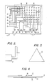
- Fig. 1 illustrates a section of the terminal pad metal layer which is deposited on a semiconductor chip 10 after the device fabrication and interconnection processes are completed.
- the type of and processes for making the semiconductor devices are not critical to this invention, nor are the methods of interconnecting the devices.
- the integrated circuit can have 1, 2, 3 or any number of metal interconnect layers under the pad level metal.
- the terminal pad metal level includes via pads 12 along the periphery of the chip 10. Via pads 12 connect through one or more underlying layers (not shown) down to underlying devices and interconnection metallurgy. Metal lines 14 carry the electrical signals from the via pads 12 to an array of terminal pads shown within the dotted area 16.
- ⁇ Within the area 16 are functional terminal pads 18 that will carry electrical signals to and from the chip 10. These functional pads 18 have a first shape which is square in the preferred embodiment. Also, within the pad array area 16 are non-functional terminal pads 20 which have a second shape which is easily distinguishable from the first square shape. In the preferred embodiment, this shape is triangular.
- Fig. 2 shows a blown-up functional terminal pad 18 with metal line 14 connecting it to a via pad (not shown).
- Fig. 3 shows a non-functional triangular terminal pad 20. Since pad 20 is non-functional, i.e., there are no inputs or outputs to it, there is no corresponding metal line attached.
- the process for depositing the pad metal level is the same as currently practiced in the art. The only difference is that the mask used to define the pad level metal has both triangular and square terminal pad shapes, rather than just one shape as currently practiced. Also, the choice of materials is the same as practiced in the art is are of no significance to This invention.
- the entire semiconductor chip is coated with a passivation/insulation layer such as polyimide.
- a passivation/insulation layer such as polyimide.
- Other passivation/insulation layers can be used, but it is preferable to use a material that is easily applied and is transparent.
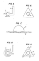
- the semiconductor chip 10 includes the terminal pad 20 which, in this case is a triangular, non-functional pad 20.
- the polyimide passivation/insulation layer 22 Applied over the pad metal layer.
- the terminal via 24 through the polyimide layer 22. The steps for this process are beyond the scope of this invention. After etching the via 24, the functional terminal pads 18 and non-functional pads 20 would appear as in Figs. 5 and 6, respectively.
- the ball limiting metallurgy 26 is deposited through appropriate masks.
- the ball limiting metallurgy which can comprise chrome, copper, titanium, gold, nickel, tungsten or any other metals conventionally used for interconnection, makes contact through the via 24 down to the underlying terminal pads 20 or 18.
- Figs. 8 and 9 illustrate the relative dimensions of the ball limiting metallurgy 24 with respect to the functional terminal pad 18 and non-functional pad 20.
- the ball limiting metallurgy 24 will define the dimensions of the solder balls which are subsequently deposited.
- the solder balls are deposited in a manner wellknown in the art, one method of which is disclosed in U.S. Patent 4,290,079, which is commonly assigned to the assignee of this invention and is hereby incorporated by reference.
- the cross-section of the semiconductor chip 10 appears as is shown in Fig. 7.
Landscapes
- Engineering & Computer Science (AREA)
- Microelectronics & Electronic Packaging (AREA)
- Internal Circuitry In Semiconductor Integrated Circuit Devices (AREA)
- Semiconductor Integrated Circuits (AREA)
Applications Claiming Priority (2)
| Application Number | Priority Date | Filing Date | Title |
|---|---|---|---|
| US3419887A | 1987-04-06 | 1987-04-06 | |
| US34198 | 1987-04-06 |
Publications (2)
| Publication Number | Publication Date |
|---|---|
| EP0285820A2 true EP0285820A2 (fr) | 1988-10-12 |
| EP0285820A3 EP0285820A3 (fr) | 1990-06-13 |
Family
ID=21874908
Family Applications (1)
| Application Number | Title | Priority Date | Filing Date |
|---|---|---|---|
| EP88103369A Withdrawn EP0285820A3 (fr) | 1987-04-06 | 1988-03-04 | Procédé et structure pour identifier des plages de connexion non fonctionnelles pour puces |
Country Status (2)
| Country | Link |
|---|---|
| EP (1) | EP0285820A3 (fr) |
| JP (1) | JPS63261842A (fr) |
Cited By (5)
| Publication number | Priority date | Publication date | Assignee | Title |
|---|---|---|---|---|
| EP0402592A3 (fr) * | 1989-06-13 | 1991-07-24 | Kabushiki Kaisha Toshiba | Dispositif semi-conducteur à circuit prédiffusé et son procédé de fabrication |
| FR2680278A1 (fr) * | 1991-08-08 | 1993-02-12 | Gemplus Card Int | Circuit integre et utilisation dans un module a plusieurs puces de circuit integre. |
| US6212077B1 (en) | 1999-01-25 | 2001-04-03 | International Business Machines Corporation | Built-in inspection template for a printed circuit |
| CN102692526A (zh) * | 2011-03-23 | 2012-09-26 | 鸿富锦精密工业(深圳)有限公司 | 辅助测试装置 |
| US20120246371A1 (en) * | 2011-03-23 | 2012-09-27 | Hon Hai Precision Industry Co., Ltd. | Test apparatus for pci card |
Family Cites Families (2)
| Publication number | Priority date | Publication date | Assignee | Title |
|---|---|---|---|---|
| FR1602834A (fr) * | 1968-12-31 | 1971-02-01 | ||
| JPS604249A (ja) * | 1983-06-22 | 1985-01-10 | Nec Corp | 半導体装置 |
-
1988
- 1988-02-03 JP JP63022181A patent/JPS63261842A/ja active Pending
- 1988-03-04 EP EP88103369A patent/EP0285820A3/fr not_active Withdrawn
Cited By (7)
| Publication number | Priority date | Publication date | Assignee | Title |
|---|---|---|---|---|
| EP0402592A3 (fr) * | 1989-06-13 | 1991-07-24 | Kabushiki Kaisha Toshiba | Dispositif semi-conducteur à circuit prédiffusé et son procédé de fabrication |
| FR2680278A1 (fr) * | 1991-08-08 | 1993-02-12 | Gemplus Card Int | Circuit integre et utilisation dans un module a plusieurs puces de circuit integre. |
| US6212077B1 (en) | 1999-01-25 | 2001-04-03 | International Business Machines Corporation | Built-in inspection template for a printed circuit |
| US6514777B2 (en) | 1999-01-25 | 2003-02-04 | International Business Machines Corporation | Built-in inspection template for a printed circuit |
| CN102692526A (zh) * | 2011-03-23 | 2012-09-26 | 鸿富锦精密工业(深圳)有限公司 | 辅助测试装置 |
| US20120246371A1 (en) * | 2011-03-23 | 2012-09-27 | Hon Hai Precision Industry Co., Ltd. | Test apparatus for pci card |
| US20120242362A1 (en) * | 2011-03-23 | 2012-09-27 | Hon Hai Precision Industry Co., Ltd. | Test apparatus |
Also Published As
| Publication number | Publication date |
|---|---|
| JPS63261842A (ja) | 1988-10-28 |
| EP0285820A3 (fr) | 1990-06-13 |
Similar Documents
| Publication | Publication Date | Title |
|---|---|---|
| US4446477A (en) | Multichip thin film module | |
| US12100679B2 (en) | Multi-pin-wafer-level-chip-scale-packaging solution for high power semiconductor devices | |
| US6277669B1 (en) | Wafer level packaging method and packages formed | |
| US5010389A (en) | Integrated circuit substrate with contacts thereon for a packaging structure | |
| US5244833A (en) | Method for manufacturing an integrated circuit chip bump electrode using a polymer layer and a photoresist layer | |
| US6221750B1 (en) | Fabrication of deformable leads of microelectronic elements | |
| EP1374306B1 (fr) | Tiges metallurgiques a bosses pour le routage de la mise a la terre et de la puissance | |
| US5847466A (en) | Semiconductor device and manufacturing method for the same | |
| DE69915299T2 (de) | Methode um lötzinn auf eine anordnung zu übertragen und/oder die anordnung zu testen | |
| EP0171662A2 (fr) | Procédé pour fabriquer des couches d'interposition pour chip | |
| KR20050085387A (ko) | 집적 회로의 검사를 수행하기 위한 소켓을 제조하는 방법및 제조된 소켓 | |
| US20100297841A1 (en) | Method for providing a redistribution metal layer in an integrated circuit | |
| EP0145862A2 (fr) | Métallisation d'un substrat céramique | |
| KR100733525B1 (ko) | 상호 접속 조립체 및 방법 | |
| EP0285820A2 (fr) | Procédé et structure pour identifier des plages de connexion non fonctionnelles pour puces | |
| US6291268B1 (en) | Low cost method of testing a cavity-up BGA substrate | |
| KR100837446B1 (ko) | 반도체 장치 및 그 제조 방법 | |
| US7411135B2 (en) | Contour structures to highlight inspection regions | |
| JP4592634B2 (ja) | 半導体装置 | |
| US6429390B1 (en) | Structure and method for forming the same of a printed wiring board having built-in inspection aids | |
| CN121547942A (zh) | 邦定线路板、邦定线路板的制作方法及显示装置 | |
| JP2006222103A (ja) | 半導体ウェハおよびその製造方法ならびに半導体ウェハの検査方法 | |
| JP3128200B2 (ja) | 電子回路基板の検査方法 | |
| JPH06326109A (ja) | 半導体装置のパッド構造およびそれを用いた特性試験方法 | |
| JPS599938A (ja) | 半導体装置 |
Legal Events
| Date | Code | Title | Description |
|---|---|---|---|
| PUAI | Public reference made under article 153(3) epc to a published international application that has entered the european phase |
Free format text: ORIGINAL CODE: 0009012 |
|
| AK | Designated contracting states |
Kind code of ref document: A2 Designated state(s): DE FR GB |
|
| 17P | Request for examination filed |
Effective date: 19890222 |
|
| PUAL | Search report despatched |
Free format text: ORIGINAL CODE: 0009013 |
|
| AK | Designated contracting states |
Kind code of ref document: A3 Designated state(s): DE FR GB |
|
| STAA | Information on the status of an ep patent application or granted ep patent |
Free format text: STATUS: THE APPLICATION IS DEEMED TO BE WITHDRAWN |
|
| 18D | Application deemed to be withdrawn |
Effective date: 19901214 |