EP0285854A1 - Condensateur à film mince - Google Patents
Condensateur à film mince Download PDFInfo
- Publication number
- EP0285854A1 EP0285854A1 EP88103915A EP88103915A EP0285854A1 EP 0285854 A1 EP0285854 A1 EP 0285854A1 EP 88103915 A EP88103915 A EP 88103915A EP 88103915 A EP88103915 A EP 88103915A EP 0285854 A1 EP0285854 A1 EP 0285854A1
- Authority
- EP
- European Patent Office
- Prior art keywords
- capacitor
- metal
- conductors
- separated
- thin film
- Prior art date
- Legal status (The legal status is an assumption and is not a legal conclusion. Google has not performed a legal analysis and makes no representation as to the accuracy of the status listed.)
- Granted
Links
- 239000003990 capacitor Substances 0.000 title claims abstract description 57
- 239000010409 thin film Substances 0.000 title claims abstract description 12
- 239000004020 conductor Substances 0.000 claims abstract description 35
- 229910052751 metal Inorganic materials 0.000 claims abstract description 29
- 239000002184 metal Substances 0.000 claims abstract description 29
- 239000010408 film Substances 0.000 claims abstract description 14
- 239000000758 substrate Substances 0.000 claims abstract description 11
- 238000000151 deposition Methods 0.000 claims abstract description 3
- 239000012212 insulator Substances 0.000 claims description 26
- 239000011248 coating agent Substances 0.000 claims description 12
- 238000000576 coating method Methods 0.000 claims description 12
- 229910052758 niobium Inorganic materials 0.000 claims description 12
- 239000010955 niobium Substances 0.000 claims description 12
- GUCVJGMIXFAOAE-UHFFFAOYSA-N niobium atom Chemical compound [Nb] GUCVJGMIXFAOAE-UHFFFAOYSA-N 0.000 claims description 12
- 238000000034 method Methods 0.000 claims description 10
- 229910052715 tantalum Inorganic materials 0.000 claims description 6
- GUVRBAGPIYLISA-UHFFFAOYSA-N tantalum atom Chemical compound [Ta] GUVRBAGPIYLISA-UHFFFAOYSA-N 0.000 claims description 6
- 238000007743 anodising Methods 0.000 claims description 2
- 239000003989 dielectric material Substances 0.000 abstract description 4
- 239000004065 semiconductor Substances 0.000 abstract description 4
- 230000007547 defect Effects 0.000 description 9
- 238000005530 etching Methods 0.000 description 4
- RYGMFSIKBFXOCR-UHFFFAOYSA-N Copper Chemical compound [Cu] RYGMFSIKBFXOCR-UHFFFAOYSA-N 0.000 description 3
- 229910052802 copper Inorganic materials 0.000 description 3
- 239000010949 copper Substances 0.000 description 3
- 229910052782 aluminium Inorganic materials 0.000 description 2
- XAGFODPZIPBFFR-UHFFFAOYSA-N aluminium Chemical compound [Al] XAGFODPZIPBFFR-UHFFFAOYSA-N 0.000 description 2
- 238000004519 manufacturing process Methods 0.000 description 2
- BPUBBGLMJRNUCC-UHFFFAOYSA-N oxygen(2-);tantalum(5+) Chemical compound [O-2].[O-2].[O-2].[O-2].[O-2].[Ta+5].[Ta+5] BPUBBGLMJRNUCC-UHFFFAOYSA-N 0.000 description 2
- 229910001936 tantalum oxide Inorganic materials 0.000 description 2
- LFQSCWFLJHTTHZ-UHFFFAOYSA-N Ethanol Chemical compound CCO LFQSCWFLJHTTHZ-UHFFFAOYSA-N 0.000 description 1
- 238000010276 construction Methods 0.000 description 1
- 230000000694 effects Effects 0.000 description 1
- 230000000873 masking effect Effects 0.000 description 1
- 150000002739 metals Chemical class 0.000 description 1
- 229910000484 niobium oxide Inorganic materials 0.000 description 1
- URLJKFSTXLNXLG-UHFFFAOYSA-N niobium(5+);oxygen(2-) Chemical compound [O-2].[O-2].[O-2].[O-2].[O-2].[Nb+5].[Nb+5] URLJKFSTXLNXLG-UHFFFAOYSA-N 0.000 description 1
- 230000003647 oxidation Effects 0.000 description 1
- 238000007254 oxidation reaction Methods 0.000 description 1
- TWNQGVIAIRXVLR-UHFFFAOYSA-N oxo(oxoalumanyloxy)alumane Chemical compound O=[Al]O[Al]=O TWNQGVIAIRXVLR-UHFFFAOYSA-N 0.000 description 1
- 230000003071 parasitic effect Effects 0.000 description 1
- 238000000206 photolithography Methods 0.000 description 1
- 229920002120 photoresistant polymer Polymers 0.000 description 1
- 238000000926 separation method Methods 0.000 description 1
Images


Classifications
-
- H—ELECTRICITY
- H10—SEMICONDUCTOR DEVICES; ELECTRIC SOLID-STATE DEVICES NOT OTHERWISE PROVIDED FOR
- H10D—INORGANIC ELECTRIC SEMICONDUCTOR DEVICES
- H10D1/00—Resistors, capacitors or inductors
- H10D1/60—Capacitors
- H10D1/68—Capacitors having no potential barriers
-
- Y—GENERAL TAGGING OF NEW TECHNOLOGICAL DEVELOPMENTS; GENERAL TAGGING OF CROSS-SECTIONAL TECHNOLOGIES SPANNING OVER SEVERAL SECTIONS OF THE IPC; TECHNICAL SUBJECTS COVERED BY FORMER USPC CROSS-REFERENCE ART COLLECTIONS [XRACs] AND DIGESTS
- Y10—TECHNICAL SUBJECTS COVERED BY FORMER USPC
- Y10T—TECHNICAL SUBJECTS COVERED BY FORMER US CLASSIFICATION
- Y10T29/00—Metal working
- Y10T29/43—Electric condenser making
- Y10T29/435—Solid dielectric type
Definitions
- Integrated thin film capacitors are desirable for power supply regulation of high performance electronic devices such as MOS and bipolar chips and other types of semiconductors. Specific capacitance required now is in the order of 50 nF/cm2, and is expected to increase as still higher performance electronics become available. Integrating the capacitor into the substrate (on which the chips are mounted or which provides the interconnect between chips) is desirable because it would provide more usable area for the devices and would minimize the parasitic inductance between the chips and the capacitor. Even preferable would be to integrate the capacitor directly onto the chips themselves. However, the prime problem in fabricating such a capacitor is in the presence of point defects which short out the capacitor.
- the present invention describes an apparatus and method for fabricating capacitors with specific capacitance much higher than is required near term, with high yield.
- the basic principle is to fabricate two capacitors in series: M1-I1-M2-I2-M3, where M refers to metal and I refers to a thin, high dielectric constant insulator.
- M2 refers to metal
- I refers to a thin, high dielectric constant insulator.
- the middle metal film M2 is patterned into many, for example, a million, of individual isolated regions.
- This structure then provides a plurality of small area capacitors connected in parallel in which each capacitor consists of two capacitors in series. The entire structure will then be good so long as there are no simultaneous defects in both I1 and I2 at the same small area capacitor.
- the present invention is directed to an integrated thin film capacitor which includes first, second and third metallic conductor layers in which the first and second layers are separated by a first insulator layer, and the second and third layers are separated by a second insulator layer.
- the first and third conductors are continuous conductors and the second conductor is positioned between the first and second conductors and is a plurality of separated conductors whereby the three conductor layers form a plurality of two series connected capacitors which are all connected in parallel.
- Still a further object of the present invention is wherein the integrated capacitor is formed as part of an electrical substrate wafer or directly integrated on integrated circuit chips.
- metallic conductors include niobium or tantalum.
- Yet a still further object of the present invention is the method of making a capacitor on an electronic substrate wafer including coating a substrate with a first thin film of metal, applying a first dielectric coating over the first metal film, fabricating a plurality of separated and spaced metal films on the dielectric coating, placing a second dielectric coating over the plurality of spaced metal films, and applying a second thin film of metal over the second dielectric coating.
- Still a further object is wherein the plurality of spaced metal films are formed by depositing a coating of metal and anodizing spaced portions of the coating of metal.
- the present invention will be described, for purposes of illustration only, as forming an integral part of an electronic substrate such as a semiconductor chip or an interconnect substrate, the invention may be fabricated by other methods and be used in other applications.
- the present invention is particularly advantageous in its use in the power supply of a high performance chip to provide a substantially constant voltage.
- capacitors are mounted as close as possible to the chips and the present capacitor would have the advantage of minimizing electrical noise and increasing the performance of the chip.
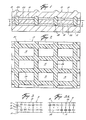
- the capacitor of the present invention is generally indicated by the reference numeral 10 and includes several thin films of alternating conductors and insulators.
- the capacitor may include a first metallic conductor layer 12 such as niobium or tantalum of a suitable thickness, for example, 5000 Angstroms.
- a middle layer 14 of a metallic conductor is provided which is formed in a plurality of spaced and separated conductors 16, for example of a thickness of 1000 Angstroms and a cross-sectional area of (40 um)2 with 10um separation between the conductors 16.
- a third metallic conductor layer 18 is provided, for example, of a thickness of 5000 Angstroms.
- a first thin high dielectric constant insulator such as niobium oxide or tantalum oxide is provided between the metallic conductors 12 and 14.
- a second high dielectric constant insulator 22 is provided between the second layer 16 and the third layer 18 of the metallic conductors.
- the layers 20 and 22 may be of a thickness of 500 Angstroms and may be an oxide of the metal conductors used.
- the discrete conductors 16 are separated from each other by a dielectric 24 such as an anodized metal.
- the cross-sectional area of the capacitor 10 could be 100 cm2.
- the first 12 and third metal layers 18 may be patterned if desired, in the same manner in which a conventional capacitor may have patterned electrodes. Furthermore, electrical connection to the first or third metal layers 12 and 18 may be made by, for example etching, through both insulator layers and the middle electrode, again in substantially the same manner by which electrial contact can be made to both layers of a conventional capacitor.
- the capacitor 10 of the present invention as best seen in the schematic in Fig. 3, consists of a plurality of two series connected capacitors in which the plurality of series connected capacitors are connected in parallel.
- the problem in fabricating such a conductor 10 is that the insulating layers 20 and 22 are very thin and it is difficult to maintain and fabricate such insulators so as to prevent shorts in the capacitor 10.
- the capacitor 10 of the present invention is defect insensitive. That is, assuming that a defect 26 and 28 or a short occurs in the capacitor 10, the defects do not short the overall capacitor 10 unless they both occur in the same two capacitors in series.
- the capacitor 10 may be formed by typical layering techniques, such as used in the semiconductor art involving alternating layers of conductors and insulators and by the use of photolithography and/or etching.
- a layer or film 12 of niobium is formed, as best seen in Fig. 4A, and as best seen in Fig. 4B is partially anodized or thermally oxidized to form a high dielectric insulator layer 20.
- the insulator 20 is then coated with a layer of niobium.
- a conventional photoresist mask (not shown) is applied to the top surface of the layer 14, and a pattern is photolithographically printed on the resist mask, the resist mask is developed and cured, all as is conventional, to cover what will be the discrete conductors 16, as best seen in Fig. 4D, and the bare portions are anodized through the entire thickness of the second niobium layer, to form the insulator portions 24. It is important that the spaces between the patterned middle electrodes 46 are filled with a thick insulator; otherwise those regions would be subject to shorts. Referring to 4E, the remaining niobium of layer 14 is partially anodized or thermally oxidized to provide the dielectric insulator layer 22. And as best seen in Fig. 4F a thin film of niobium metal 18 is applied on the top of the insulator layer 22 to complete the capacitor 10.
- metals and insulator layers may be used.
- tantalum may be used for the metallic conductor layers 12, 14 and 18 and the insulators 20, 22 and 24 may use tantalum oxide.
- other methods of forming the metal conductors and insulators may be used, such as masking, and etching.
- the layers 20 and 22 could be formed of other oxides or by other methods such as thermal oxidation.
- a capacitor 10a is fabricated using a first metallic conductor layer 40 which may be copper, a second layer of 42 of niobium whereby the layer of copper 40 could provide a low sheet resistance for the capacitor electrodes.
- An insulator layer 44 is provided which may be aluminum which can then be anodized to provide aluminum oxide.
- the second layer of metallic conductor 42 may be niobium or tantalum which may be patterned into the desired separated and spaced conductor segments 46 by etching.
- a second insulator layer 48 may be aluminum which is anodized into an oxide.
- Another layer of niobium 50 is provided and connected to a top layer of copper 52 for providing a low resistance.
Landscapes
- Fixed Capacitors And Capacitor Manufacturing Machines (AREA)
- Semiconductor Integrated Circuits (AREA)
- Parts Printed On Printed Circuit Boards (AREA)
Applications Claiming Priority (2)
| Application Number | Priority Date | Filing Date | Title |
|---|---|---|---|
| US07/036,398 US4890192A (en) | 1987-04-09 | 1987-04-09 | Thin film capacitor |
| US36398 | 1987-04-09 |
Publications (2)
| Publication Number | Publication Date |
|---|---|
| EP0285854A1 true EP0285854A1 (fr) | 1988-10-12 |
| EP0285854B1 EP0285854B1 (fr) | 1992-09-23 |
Family
ID=21888399
Family Applications (1)
| Application Number | Title | Priority Date | Filing Date |
|---|---|---|---|
| EP88103915A Expired - Lifetime EP0285854B1 (fr) | 1987-04-09 | 1988-03-11 | Condensateur à film mince |
Country Status (4)
| Country | Link |
|---|---|
| US (1) | US4890192A (fr) |
| EP (1) | EP0285854B1 (fr) |
| JP (1) | JPS63266809A (fr) |
| DE (1) | DE3874785T2 (fr) |
Cited By (1)
| Publication number | Priority date | Publication date | Assignee | Title |
|---|---|---|---|---|
| US6933551B1 (en) | 2002-04-05 | 2005-08-23 | Zarlink Semiconductor Limited | Large value, compact, high yielding integrated circuit capacitors |
Families Citing this family (18)
| Publication number | Priority date | Publication date | Assignee | Title |
|---|---|---|---|---|
| US5027253A (en) * | 1990-04-09 | 1991-06-25 | Ibm Corporation | Printed circuit boards and cards having buried thin film capacitors and processing techniques for fabricating said boards and cards |
| US5120572A (en) * | 1990-10-30 | 1992-06-09 | Microelectronics And Computer Technology Corporation | Method of fabricating electrical components in high density substrates |
| US5254493A (en) * | 1990-10-30 | 1993-10-19 | Microelectronics And Computer Technology Corporation | Method of fabricating integrated resistors in high density substrates |
| US5817533A (en) * | 1996-07-29 | 1998-10-06 | Fujitsu Limited | High-yield methods of fabricating large substrate capacitors |
| US5917230A (en) * | 1997-04-09 | 1999-06-29 | United Memories, Inc. | Filter capacitor construction |
| US6137671A (en) * | 1998-01-29 | 2000-10-24 | Energenius, Inc. | Embedded energy storage device |
| US6226171B1 (en) | 1998-04-27 | 2001-05-01 | Fujitsu Limited | Power conducting substrates with high-yield integrated substrate capacitor |
| EP1123565B1 (fr) * | 1998-10-02 | 2011-08-17 | Raytheon Company | Modules multi-puce avec condensateurs enterrés |
| US6466427B1 (en) | 2000-05-31 | 2002-10-15 | Taiwan Semiconductor Manufacturing Co., Ltd. | Microelectronic capacitor structure compatible with copper containing microelectronic conductor layer processing |
| US6980414B1 (en) | 2004-06-16 | 2005-12-27 | Marvell International, Ltd. | Capacitor structure in a semiconductor device |
| US9572258B2 (en) * | 2004-12-30 | 2017-02-14 | Intel Corporation | Method of forming a substrate core with embedded capacitor and structures formed thereby |
| US7372126B2 (en) * | 2005-03-31 | 2008-05-13 | Intel Corporation | Organic substrates with embedded thin-film capacitors, methods of making same, and systems containing same |
| US7288459B2 (en) * | 2005-03-31 | 2007-10-30 | Intel Corporation | Organic substrates with integral thin-film capacitors, methods of making same, and systems containing same |
| DE102005056906B4 (de) * | 2005-11-29 | 2010-01-07 | Infineon Technologies Ag | Integrierte Schaltungsanordnung mit in Reihe geschalteten Kondensatoren und Verwendung |
| JP4973023B2 (ja) * | 2006-06-19 | 2012-07-11 | 日本電気株式会社 | 薄膜キャパシタ及びその製造方法 |
| CN102543438B (zh) * | 2011-12-07 | 2014-04-16 | 厦门法拉电子股份有限公司 | 一种叠片式金属化薄膜电容器的电极结构 |
| CN104916439A (zh) * | 2015-05-10 | 2015-09-16 | 长兴华强电子有限公司 | 耐高温微型高压电容器 |
| CN106252075A (zh) * | 2016-08-11 | 2016-12-21 | 苏州柯创电子材料有限公司 | 金属化薄膜电容的制造工艺 |
Citations (1)
| Publication number | Priority date | Publication date | Assignee | Title |
|---|---|---|---|---|
| EP0098671A1 (fr) * | 1982-07-09 | 1984-01-18 | R.T.C. LA RADIOTECHNIQUE-COMPELEC Société anonyme dite: | Procédé d'isolement par oxydation anodique de portions métalliques entre elles et dispositif obtenu par ce procédé |
Family Cites Families (17)
| Publication number | Priority date | Publication date | Assignee | Title |
|---|---|---|---|---|
| US3257592A (en) * | 1966-06-21 | Silicon monoxide | ||
| US3113253A (en) * | 1958-09-22 | 1963-12-03 | Nippon Electric Co | Capacitors |
| US3603850A (en) * | 1969-11-14 | 1971-09-07 | Mallory & Co Inc P R | Ceramic capacitor with counterelectrode |
| JPS505591B1 (fr) * | 1970-02-04 | 1975-03-05 | ||
| US3745430A (en) * | 1971-12-21 | 1973-07-10 | Motorola Inc | Thick film feed-through capacitor |
| US3778689A (en) * | 1972-05-22 | 1973-12-11 | Hewlett Packard Co | Thin film capacitors and method for manufacture |
| US3882059A (en) * | 1973-05-11 | 1975-05-06 | Technical Ceramics Inc | Method of making ceramic capacitor |
| US4238762A (en) * | 1974-04-22 | 1980-12-09 | Rockwell International Corporation | Electrically isolated semiconductor devices on common crystalline substrate |
| JPS51116967A (en) * | 1975-04-08 | 1976-10-14 | Shinnitsutoku Denki Kk | Silver mica block capacitor |
| US4074340A (en) * | 1976-10-18 | 1978-02-14 | Vitramon, Incorporated | Trimmable monolithic capacitors |
| US4136291A (en) * | 1977-05-23 | 1979-01-23 | General Electric Company | Capacitive touch-pad devices with dynamic bias |
| US4190854A (en) * | 1978-02-15 | 1980-02-26 | National Semiconductor Corporation | Trim structure for integrated capacitors |
| US4347650A (en) * | 1980-09-22 | 1982-09-07 | Avx Corporation | Method of making marginless multi-layer ceramic capacitors |
| US4401843A (en) * | 1981-03-31 | 1983-08-30 | Rogers Corporation | Miniaturized bus bars and methods of fabrication thereof |
| JPS57178353A (en) * | 1981-04-27 | 1982-11-02 | Alps Electric Co Ltd | Thick film printed circuit |
| DE3235772A1 (de) * | 1981-09-30 | 1983-06-23 | Matsushita Electric Industrial Co., Ltd., Kadoma, Osaka | Mehrschichtkondensator |
| US4527180A (en) * | 1983-01-31 | 1985-07-02 | Intel Corporation | MOS Voltage divider structure suitable for higher potential feedback regulation |
-
1987
- 1987-04-09 US US07/036,398 patent/US4890192A/en not_active Expired - Lifetime
-
1988
- 1988-03-11 EP EP88103915A patent/EP0285854B1/fr not_active Expired - Lifetime
- 1988-03-11 DE DE8888103915T patent/DE3874785T2/de not_active Expired - Fee Related
- 1988-04-08 JP JP63087058A patent/JPS63266809A/ja active Pending
Patent Citations (1)
| Publication number | Priority date | Publication date | Assignee | Title |
|---|---|---|---|---|
| EP0098671A1 (fr) * | 1982-07-09 | 1984-01-18 | R.T.C. LA RADIOTECHNIQUE-COMPELEC Société anonyme dite: | Procédé d'isolement par oxydation anodique de portions métalliques entre elles et dispositif obtenu par ce procédé |
Non-Patent Citations (2)
| Title |
|---|
| IBM TECHNICAL DISCLOSURE BULLETIN, vol. 25, no. 11A, April 1983, page 5545, New York, US; D.B. DOVE et al.: "Protective electrode for a large-area capacitor structure" * |
| IBM TECHNICAL DISCLOSURE BULLETIN, vol. 9, no. 10, March 1967, page 1266, New York, US; A.S. FARBER: "High-capacitance power distribution network" * |
Cited By (1)
| Publication number | Priority date | Publication date | Assignee | Title |
|---|---|---|---|---|
| US6933551B1 (en) | 2002-04-05 | 2005-08-23 | Zarlink Semiconductor Limited | Large value, compact, high yielding integrated circuit capacitors |
Also Published As
| Publication number | Publication date |
|---|---|
| DE3874785D1 (en) | 1992-10-29 |
| US4890192A (en) | 1989-12-26 |
| DE3874785T2 (de) | 1993-03-18 |
| EP0285854B1 (fr) | 1992-09-23 |
| JPS63266809A (ja) | 1988-11-02 |
Similar Documents
| Publication | Publication Date | Title |
|---|---|---|
| US4890192A (en) | Thin film capacitor | |
| CA1182583A (fr) | Condensateur de decouplage discret a film mince | |
| EP0899992B1 (fr) | Procédé de fabrication d'un circuit imprimé multicouches comprenant des composants encastrés passifs à couche mince | |
| JP3980658B2 (ja) | 薄膜コンデンサの形成方法、薄膜コンデンサの製造方法、薄膜バイパスコンデンサの製造方法および薄膜コンデンサ | |
| US6678144B2 (en) | Capacitor, circuit board with built-in capacitor and method for producing the same | |
| US6524352B2 (en) | Method of making a parallel capacitor laminate | |
| US6452776B1 (en) | Capacitor with defect isolation and bypass | |
| US5946600A (en) | Method for manufacturing an electronic structure | |
| GB2119570A (en) | Integrated capacitor manufacture | |
| US6262478B1 (en) | Electronic interconnect structure and method for manufacturing it | |
| JP2004507105A (ja) | 受動素子を有する半導体デバイスおよびそれを作製する方法 | |
| KR20010006086A (ko) | 집적 회로의 커패시터 | |
| KR20010039886A (ko) | 반도체 장치 | |
| JPH0878283A (ja) | 薄膜キャパシタ | |
| US7282419B2 (en) | Thin-film capacitor device, mounting module for the same, and method for fabricating the same | |
| US6830984B2 (en) | Thick traces from multiple damascene layers | |
| US7005722B2 (en) | RC terminator and production method therefor | |
| US20050056939A1 (en) | Thin-film capacitor and method of producing the capacitor | |
| JPH0247862A (ja) | 半導体集積回路装置 | |
| US5420068A (en) | Semiconductor integrated circuit and a method for manufacturing a fully planar multilayer wiring structure | |
| EP1093163A2 (fr) | Structure d'interconnexion électronique | |
| JP2003234245A (ja) | 多層キャパシタ及びその製造方法 | |
| US6645804B1 (en) | System for fabricating a metal/anti-reflective coating/insulator/metal (MAIM) capacitor | |
| US6348393B1 (en) | Capacitor in an integrated circuit and a method of manufacturing an integrated circuit | |
| KR930009579B1 (ko) | 반도체 기억장치의 적층캐패시터 제조방법 |
Legal Events
| Date | Code | Title | Description |
|---|---|---|---|
| PUAI | Public reference made under article 153(3) epc to a published international application that has entered the european phase |
Free format text: ORIGINAL CODE: 0009012 |
|
| AK | Designated contracting states |
Kind code of ref document: A1 Designated state(s): DE FR GB |
|
| 17P | Request for examination filed |
Effective date: 19890403 |
|
| 17Q | First examination report despatched |
Effective date: 19910423 |
|
| GRAA | (expected) grant |
Free format text: ORIGINAL CODE: 0009210 |
|
| AK | Designated contracting states |
Kind code of ref document: B1 Designated state(s): DE FR GB |
|
| REF | Corresponds to: |
Ref document number: 3874785 Country of ref document: DE Date of ref document: 19921029 |
|
| ET | Fr: translation filed | ||
| PLBE | No opposition filed within time limit |
Free format text: ORIGINAL CODE: 0009261 |
|
| STAA | Information on the status of an ep patent application or granted ep patent |
Free format text: STATUS: NO OPPOSITION FILED WITHIN TIME LIMIT |
|
| 26N | No opposition filed | ||
| PGFP | Annual fee paid to national office [announced via postgrant information from national office to epo] |
Ref country code: GB Payment date: 19940221 Year of fee payment: 7 |
|
| PGFP | Annual fee paid to national office [announced via postgrant information from national office to epo] |
Ref country code: FR Payment date: 19940318 Year of fee payment: 7 |
|
| PGFP | Annual fee paid to national office [announced via postgrant information from national office to epo] |
Ref country code: DE Payment date: 19940525 Year of fee payment: 7 |
|
| PG25 | Lapsed in a contracting state [announced via postgrant information from national office to epo] |
Ref country code: GB Effective date: 19950311 |
|
| GBPC | Gb: european patent ceased through non-payment of renewal fee |
Effective date: 19950311 |
|
| PG25 | Lapsed in a contracting state [announced via postgrant information from national office to epo] |
Ref country code: FR Free format text: LAPSE BECAUSE OF NON-PAYMENT OF DUE FEES Effective date: 19951130 |
|
| PG25 | Lapsed in a contracting state [announced via postgrant information from national office to epo] |
Ref country code: DE Effective date: 19951201 |
|
| REG | Reference to a national code |
Ref country code: FR Ref legal event code: ST |