EP0286106A2 - Verfahren zur Herstellung eines supraleitenden Elements - Google Patents
Verfahren zur Herstellung eines supraleitenden Elements Download PDFInfo
- Publication number
- EP0286106A2 EP0286106A2 EP88105573A EP88105573A EP0286106A2 EP 0286106 A2 EP0286106 A2 EP 0286106A2 EP 88105573 A EP88105573 A EP 88105573A EP 88105573 A EP88105573 A EP 88105573A EP 0286106 A2 EP0286106 A2 EP 0286106A2
- Authority
- EP
- European Patent Office
- Prior art keywords
- superconductive
- oxide
- oxygen
- layer
- oxides
- Prior art date
- Legal status (The legal status is an assumption and is not a legal conclusion. Google has not performed a legal analysis and makes no representation as to the accuracy of the status listed.)
- Granted
Links
Images


Classifications
-
- H—ELECTRICITY
- H10—SEMICONDUCTOR DEVICES; ELECTRIC SOLID-STATE DEVICES NOT OTHERWISE PROVIDED FOR
- H10N—ELECTRIC SOLID-STATE DEVICES NOT OTHERWISE PROVIDED FOR
- H10N60/00—Superconducting devices
- H10N60/01—Manufacture or treatment
- H10N60/0268—Manufacture or treatment of devices comprising copper oxide
- H10N60/0661—Processes performed after copper oxide formation, e.g. patterning
-
- H—ELECTRICITY
- H01—ELECTRIC ELEMENTS
- H01F—MAGNETS; INDUCTANCES; TRANSFORMERS; SELECTION OF MATERIALS FOR THEIR MAGNETIC PROPERTIES
- H01F41/00—Apparatus or processes specially adapted for manufacturing or assembling magnets, inductances or transformers; Apparatus or processes specially adapted for manufacturing materials characterised by their magnetic properties
- H01F41/02—Apparatus or processes specially adapted for manufacturing or assembling magnets, inductances or transformers; Apparatus or processes specially adapted for manufacturing materials characterised by their magnetic properties for manufacturing cores, coils, or magnets
- H01F41/04—Apparatus or processes specially adapted for manufacturing or assembling magnets, inductances or transformers; Apparatus or processes specially adapted for manufacturing materials characterised by their magnetic properties for manufacturing cores, coils, or magnets for manufacturing coils
- H01F41/048—Superconductive coils
-
- H—ELECTRICITY
- H01—ELECTRIC ELEMENTS
- H01F—MAGNETS; INDUCTANCES; TRANSFORMERS; SELECTION OF MATERIALS FOR THEIR MAGNETIC PROPERTIES
- H01F6/00—Superconducting magnets; Superconducting coils
- H01F6/06—Coils, e.g. winding, insulating, terminating or casing arrangements therefor
-
- H—ELECTRICITY
- H10—SEMICONDUCTOR DEVICES; ELECTRIC SOLID-STATE DEVICES NOT OTHERWISE PROVIDED FOR
- H10N—ELECTRIC SOLID-STATE DEVICES NOT OTHERWISE PROVIDED FOR
- H10N60/00—Superconducting devices
- H10N60/01—Manufacture or treatment
- H10N60/0884—Treatment of superconductor layers by irradiation, e.g. ion-beam, electron-beam, laser beam or X-rays
-
- H—ELECTRICITY
- H10—SEMICONDUCTOR DEVICES; ELECTRIC SOLID-STATE DEVICES NOT OTHERWISE PROVIDED FOR
- H10N—ELECTRIC SOLID-STATE DEVICES NOT OTHERWISE PROVIDED FOR
- H10N60/00—Superconducting devices
- H10N60/01—Manufacture or treatment
- H10N60/0912—Manufacture or treatment of Josephson-effect devices
- H10N60/0941—Manufacture or treatment of Josephson-effect devices comprising high-Tc ceramic materials
-
- H—ELECTRICITY
- H10—SEMICONDUCTOR DEVICES; ELECTRIC SOLID-STATE DEVICES NOT OTHERWISE PROVIDED FOR
- H10N—ELECTRIC SOLID-STATE DEVICES NOT OTHERWISE PROVIDED FOR
- H10N60/00—Superconducting devices
- H10N60/20—Permanent superconducting devices
- H10N60/203—Permanent superconducting devices comprising high-Tc ceramic materials
-
- Y—GENERAL TAGGING OF NEW TECHNOLOGICAL DEVELOPMENTS; GENERAL TAGGING OF CROSS-SECTIONAL TECHNOLOGIES SPANNING OVER SEVERAL SECTIONS OF THE IPC; TECHNICAL SUBJECTS COVERED BY FORMER USPC CROSS-REFERENCE ART COLLECTIONS [XRACs] AND DIGESTS
- Y10—TECHNICAL SUBJECTS COVERED BY FORMER USPC
- Y10S—TECHNICAL SUBJECTS COVERED BY FORMER USPC CROSS-REFERENCE ART COLLECTIONS [XRACs] AND DIGESTS
- Y10S505/00—Superconductor technology: apparatus, material, process
- Y10S505/725—Process of making or treating high tc, above 30 k, superconducting shaped material, article, or device
- Y10S505/73—Vacuum treating or coating
Definitions
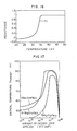
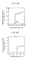
- Pellet samples of a non-superconductive YBa2Cu3O 6.2 with 25 mm in length, 6 mm in width and 3 mm in thickness were prepared by the oxide-mixing method.
- Fig. 18 is a graph showing a change of the critical temperature of the samples, as carbonic acid gas laser or electron beam is applied to the samples, with respect to the energy density applied.
- the electron beam was applied at a range of 50 to 100 keV. In both the cases of applying the electron beam and the carbonic acid gas laser, the similar results were obtained.
- the transformation from the non-superconductive form to the superconductive form began to occur at an energy density of about 1 ⁇ 102 J/cm2.
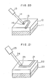
- the superconductor 13 may be used as wiring of circuits.
Landscapes
- Engineering & Computer Science (AREA)
- Power Engineering (AREA)
- Manufacturing & Machinery (AREA)
- Chemical & Material Sciences (AREA)
- Ceramic Engineering (AREA)
- Physics & Mathematics (AREA)
- Optics & Photonics (AREA)
- Inorganic Compounds Of Heavy Metals (AREA)
- Superconductor Devices And Manufacturing Methods Thereof (AREA)
- Superconductors And Manufacturing Methods Therefor (AREA)
- Compositions Of Oxide Ceramics (AREA)
- Oxygen, Ozone, And Oxides In General (AREA)
Applications Claiming Priority (8)
| Application Number | Priority Date | Filing Date | Title |
|---|---|---|---|
| JP8477087 | 1987-04-08 | ||
| JP84770/87 | 1987-04-08 | ||
| JP90762/87 | 1987-04-15 | ||
| JP9076287 | 1987-04-15 | ||
| JP93025/87 | 1987-04-17 | ||
| JP9302587 | 1987-04-17 | ||
| JP10428387 | 1987-04-30 | ||
| JP104283/87 | 1987-04-30 |
Publications (3)
| Publication Number | Publication Date |
|---|---|
| EP0286106A2 true EP0286106A2 (de) | 1988-10-12 |
| EP0286106A3 EP0286106A3 (en) | 1990-03-28 |
| EP0286106B1 EP0286106B1 (de) | 1995-08-02 |
Family
ID=27467007
Family Applications (1)
| Application Number | Title | Priority Date | Filing Date |
|---|---|---|---|
| EP88105573A Expired - Lifetime EP0286106B1 (de) | 1987-04-08 | 1988-04-07 | Verfahren zur Herstellung eines supraleitenden Elements |
Country Status (5)
| Country | Link |
|---|---|
| US (1) | US5096882A (de) |
| EP (1) | EP0286106B1 (de) |
| JP (1) | JP2876211B2 (de) |
| KR (1) | KR880013187A (de) |
| DE (1) | DE3854238T2 (de) |
Cited By (15)
| Publication number | Priority date | Publication date | Assignee | Title |
|---|---|---|---|---|
| EP0311331A3 (de) * | 1987-10-07 | 1990-02-14 | United Kingdom Atomic Energy Authority | Schaltungselemente aus supraleitender Keramik |
| EP0304807A3 (en) * | 1987-08-22 | 1990-03-21 | Sumitomo Electric Industries, Limited | Method for producing superconducting circuit |
| EP0282360A3 (en) * | 1987-03-12 | 1990-05-23 | Semiconductor Energy Laboratory Co., Ltd. | Superconducting ceramics and methods for manufacturing the same |
| FR2647266A1 (fr) * | 1989-05-17 | 1990-11-23 | Ecole Cle Arts Manufactures | Element de circuit electrique ou electronique comportant un supraconducteur sur lequel sont fixes des elements conducteurs |
| FR2670201A1 (fr) * | 1990-12-06 | 1992-06-12 | Dornier Gmbh | Procede de microstructuration de ceramiques oxydees supraconductrices. |
| US5143894A (en) * | 1987-10-14 | 1992-09-01 | Mordechai Rothschild | Formation and high resolution patterning of superconductors |
| US5194419A (en) * | 1989-07-25 | 1993-03-16 | The Furukawa Electric Co., Ltd. | Method for manufacturing an oxide superconductive multilayer circuit |
| EP0299163B1 (de) * | 1987-07-15 | 1993-12-15 | Sharp Kabushiki Kaisha | Verbindungsverfahren für Halbleiteranordnung |
| EP0292387B1 (de) * | 1987-05-18 | 1994-07-13 | Sumitomo Electric Industries Limited | Methode zur Herstellung einer supraleitenden Schaltung |
| EP0285106B1 (de) * | 1987-03-30 | 1994-08-31 | Sumitomo Electric Industries Limited | Verfahren zur Herstellung einer supraleitenden Schaltung |
| EP0290271B1 (de) * | 1987-05-08 | 1995-03-15 | Fujitsu Limited | Supraleitende Schaltungskarte und Verfahren zu ihrer Herstellung |
| WO1998024098A1 (en) * | 1996-11-27 | 1998-06-04 | British Nuclear Fuels Plc | Improvements in and relating to coils |
| WO2002027765A2 (de) | 2000-09-26 | 2002-04-04 | MAX-PLANCK-Gesellschaft zur Förderung der Wissenschaften e.V. | Stöchiometrieänderung eines ionisch aufgebauten feststoffes |
| EP1070327A4 (de) * | 1998-03-18 | 2007-05-09 | S C Power Systems Inc | Integriertes band |
| US8061016B2 (en) | 2001-08-24 | 2011-11-22 | 3-Cs Ltd | Superconducting coil fabrication |
Families Citing this family (58)
| Publication number | Priority date | Publication date | Assignee | Title |
|---|---|---|---|---|
| JPH01111702A (ja) * | 1987-10-24 | 1989-04-28 | Hiroyuki Yoshida | 複合酸化物から放射線照射を利用して室温超伝導体を製造する方法 |
| JP2965641B2 (ja) * | 1989-08-21 | 1999-10-18 | 松下電器産業株式会社 | 超伝導素子の製造方法 |
| JP2767298B2 (ja) * | 1989-09-05 | 1998-06-18 | 財団法人生産開発科学研究所 | 積層薄膜体及びその製造法 |
| JPH03151231A (ja) * | 1989-10-13 | 1991-06-27 | Internatl Business Mach Corp <Ibm> | 多層ひずみ格子銅酸化物ペロブスカイト構造体 |
| EP0478464B1 (de) * | 1990-09-27 | 1997-08-27 | Sumitomo Electric Industries, Ltd. | Herstellungsverfahren eines supraleitenden Bauelements mit extrem dünnem supraleitenden Kanal aus supraleitendem Oxidmaterial |
| DE69114435T2 (de) * | 1990-09-27 | 1996-06-13 | Sumitomo Electric Industries | Supraleitendes Bauelement und dessen Herstellungsverfahren. |
| CA2054470C (en) * | 1990-10-30 | 1997-07-01 | Takao Nakamura | Method for manufacturing superconducting device having a reduced thickness of oxide superconducting layer and superconducting device manufactured thereby |
| CA2054597C (en) * | 1990-10-31 | 1997-08-19 | Hiroshi Inada | Superconducting circuit and a process for fabricating the same |
| CA2054795C (en) * | 1990-11-01 | 1996-08-06 | Hiroshi Inada | Superconducting device having an extremely thin superconducting channel formed of oxide superconductor material and method for manufacturing the same |
| US5856275A (en) * | 1990-11-01 | 1999-01-05 | Sumitomo Electric Industries, Ltd. | Superconducting wiring lines and process for fabricating the same |
| US6308399B1 (en) * | 1991-06-18 | 2001-10-30 | Dawei Zhou | High-TC superconducting ceramic oxide products and macroscopic and microscopic methods of making the same |
| EP0591312B1 (de) * | 1991-06-24 | 1997-08-06 | Forschungszentrum Jülich Gmbh | Strukturierte leiterbahnen und verfahren zur herstellung derselben |
| JP3287028B2 (ja) * | 1991-10-25 | 2002-05-27 | 日立電線株式会社 | Tl,Pb系酸化物超電導材及びその製造方法 |
| US5747427A (en) * | 1991-11-15 | 1998-05-05 | Hokkaido Electric Power Co., Inc. | Process for forming a semiconductive thin film containing a junction |
| WO1994002862A1 (en) * | 1992-07-20 | 1994-02-03 | Superconductor Technologies, Inc. | Superconductor thin film crossovers and method |
| JPH06219736A (ja) * | 1993-01-27 | 1994-08-09 | Hitachi Ltd | 超電導体 |
| AU8070294A (en) * | 1993-07-15 | 1995-02-13 | President And Fellows Of Harvard College | Extended nitride material comprising beta -c3n4 |
| FR2714205A1 (fr) * | 1993-12-17 | 1995-06-23 | Atg Sa | Matériau composite pour l'enregistrement magnéto-optique, sa préparation et son utilisation. |
| JPH07263767A (ja) | 1994-01-14 | 1995-10-13 | Trw Inc | イオンインプランテーションを用いたプレーナ型の高温超伝導集積回路 |
| US5593918A (en) * | 1994-04-22 | 1997-01-14 | Lsi Logic Corporation | Techniques for forming superconductive lines |
| US6153561A (en) * | 1996-09-13 | 2000-11-28 | The Ohio State University | Method for oxygenating oxide superconductive materials |
| US6004508A (en) * | 1997-08-01 | 1999-12-21 | The Coca-Cola Company | Method and apparatus for super critical treatment of liquids |
| US6143366A (en) * | 1998-12-24 | 2000-11-07 | Lu; Chung Hsin | High-pressure process for crystallization of ceramic films at low temperatures |
| US6188919B1 (en) | 1999-05-19 | 2001-02-13 | Trw Inc. | Using ion implantation to create normal layers in superconducting-normal-superconducting Josephson junctions |
| US6638895B1 (en) * | 1999-10-27 | 2003-10-28 | The University Of Chicago | Method for fabricating high aspect ratio structures in perovskite material |
| JP4859165B2 (ja) * | 2004-06-07 | 2012-01-25 | 独立行政法人物質・材料研究機構 | 高臨界電流特性を有する超伝導材料及びその製造方法 |
| JPWO2006013819A1 (ja) * | 2004-08-02 | 2008-05-01 | 松下電器産業株式会社 | 抵抗変化素子とそれを用いた抵抗変化型メモリ |
| JP4431891B2 (ja) * | 2004-12-28 | 2010-03-17 | セイコーエプソン株式会社 | 圧電素子、圧電アクチュエーター、圧電ポンプ、インクジェット式記録ヘッド、インクジェットプリンター、表面弾性波素子、薄膜圧電共振子、周波数フィルタ、発振器、電子回路、および電子機器 |
| US7888290B2 (en) * | 2005-09-12 | 2011-02-15 | Armen Gulian | Material exhibiting superconductivity characteristics and method of manufacture thereof |
| JP4984466B2 (ja) * | 2005-09-21 | 2012-07-25 | 住友電気工業株式会社 | 超電導テープ線材の製造方法 |
| JP2007224747A (ja) * | 2006-02-21 | 2007-09-06 | Mitsubishi Motors Corp | ディーゼルエンジンの排ガス浄化用フィルタおよび排ガス浄化装置 |
| CN100440388C (zh) * | 2006-09-01 | 2008-12-03 | 天津理工大学 | 一种制作abo3型钙钛矿结构复氧化物离子导体的激光熔凝合成方法 |
| US7615385B2 (en) | 2006-09-20 | 2009-11-10 | Hypres, Inc | Double-masking technique for increasing fabrication yield in superconducting electronics |
| US20080146449A1 (en) * | 2006-12-14 | 2008-06-19 | Jerome Lesueur | Electrical device and method of manufacturing same |
| US8741158B2 (en) | 2010-10-08 | 2014-06-03 | Ut-Battelle, Llc | Superhydrophobic transparent glass (STG) thin film articles |
| FI126113B (fi) * | 2009-06-24 | 2016-06-30 | Johannes Frantti | Korkean lämpötilan suprajohteet |
| US20110034336A1 (en) * | 2009-08-04 | 2011-02-10 | Amit Goyal | CRITICAL CURRENT DENSITY ENHANCEMENT VIA INCORPORATION OF NANOSCALE Ba2(Y,RE)NbO6 IN REBCO FILMS |
| US20110034338A1 (en) * | 2009-08-04 | 2011-02-10 | Amit Goyal | CRITICAL CURRENT DENSITY ENHANCEMENT VIA INCORPORATION OF NANOSCALE Ba2(Y,RE)TaO6 IN REBCO FILMS |
| US9435035B2 (en) | 2010-01-15 | 2016-09-06 | Byd Company Limited | Metalized plastic articles and methods thereof |
| CN102071424B (zh) * | 2010-02-26 | 2012-05-09 | 比亚迪股份有限公司 | 一种塑料制品的制备方法及一种塑料制品 |
| US8685549B2 (en) | 2010-08-04 | 2014-04-01 | Ut-Battelle, Llc | Nanocomposites for ultra high density information storage, devices including the same, and methods of making the same |
| CN102071411B (zh) | 2010-08-19 | 2012-05-30 | 比亚迪股份有限公司 | 一种塑料制品的制备方法及一种塑料制品 |
| US11292919B2 (en) | 2010-10-08 | 2022-04-05 | Ut-Battelle, Llc | Anti-fingerprint coatings |
| US9221076B2 (en) | 2010-11-02 | 2015-12-29 | Ut-Battelle, Llc | Composition for forming an optically transparent, superhydrophobic coating |
| US8748350B2 (en) | 2011-04-15 | 2014-06-10 | Ut-Battelle | Chemical solution seed layer for rabits tapes |
| US8748349B2 (en) | 2011-04-15 | 2014-06-10 | Ut-Battelle, Llc | Buffer layers for REBCO films for use in superconducting devices |
| EP2864239B1 (de) | 2012-06-21 | 2017-12-20 | Monash University | Leitende abschnitte bei isolierenden materialien |
| CN103317240B (zh) * | 2013-07-12 | 2015-09-30 | 东明兴业科技股份有限公司 | 镁合金表面氧化层的激光蚀刻加工方法 |
| US9768370B2 (en) * | 2013-09-17 | 2017-09-19 | Varian Semiconductor Equipment Associates, Inc. | Low AC loss high temperature superconductor tape |
| US9590161B2 (en) | 2013-11-27 | 2017-03-07 | Varian Semiconductor Equipment Associates, Inc. | Laser processing of superconductor layers |
| US20150239773A1 (en) | 2014-02-21 | 2015-08-27 | Ut-Battelle, Llc | Transparent omniphobic thin film articles |
| US9543496B2 (en) * | 2014-03-17 | 2017-01-10 | Uchicago Argonne, Llc | Creation of high-pinning microstructures in post production YBCO coated conductors |
| US10283695B1 (en) * | 2016-02-29 | 2019-05-07 | The United States Of America As Represented By Secretary Of The Navy | Method for creating high-resolution micro- to nano-scale structures in high-temperature superconductor films |
| KR102145354B1 (ko) * | 2018-05-31 | 2020-08-18 | 경기대학교 산학협력단 | 양성자 빔 조사에 의한 산화 환원 사이클을 갖는 수소 생성 방법 및 이를 이용한 수소 생성 장치 |
| KR102149059B1 (ko) * | 2018-06-01 | 2020-08-28 | 경기대학교 산학협력단 | 제논광 또는 마이크로웨이브 조사에 의한 산화 환원 사이클을 갖는 수소 생성 방법 및 이를 이용한 수소 생성 장치 |
| US11783953B2 (en) * | 2018-10-02 | 2023-10-10 | Massachusetts Institute Of Technology | Cryogenic radiation enhancement of superconductors |
| CN111825444B (zh) * | 2020-08-04 | 2022-08-19 | 上海上创超导科技有限公司 | 在异位法高温超导薄膜中引入柱状缺陷的方法 |
| CN113470883B (zh) * | 2021-06-29 | 2022-11-11 | 南京大学 | 具有高临界参数无毒铜氧化物超导体及其制备方法 |
Family Cites Families (24)
| Publication number | Priority date | Publication date | Assignee | Title |
|---|---|---|---|---|
| CA631707A (en) * | 1961-11-28 | L. Ruskin Simon | Activated oxide complexes | |
| BE526937A (de) * | 1953-03-05 | 1954-09-03 | ||
| EP0008866A1 (de) * | 1978-08-11 | 1980-03-19 | LUCAS INDUSTRIES public limited company | Elektrische Schalter |
| JPS5845194B2 (ja) * | 1980-07-11 | 1983-10-07 | 日本電信電話株式会社 | 超伝導集積回路およびその製法 |
| JPS60173885A (ja) * | 1984-02-18 | 1985-09-07 | Nippon Telegr & Teleph Corp <Ntt> | 酸化物超伝導材料およびその製造方法 |
| JPS61138417A (ja) * | 1984-12-11 | 1986-06-25 | 科学技術庁金属材料技術研究所長 | A−15型超電導化合物の製造法 |
| JPS61168530A (ja) * | 1985-01-21 | 1986-07-30 | Nippon Telegr & Teleph Corp <Ntt> | 酸化物超伝導材料およびその製造方法 |
| JPS61206279A (ja) * | 1985-03-11 | 1986-09-12 | Hitachi Ltd | 超電導素子 |
| JPS62104283A (ja) * | 1985-10-31 | 1987-05-14 | Kokusai Denshin Denwa Co Ltd <Kdd> | 動画像伝送における差分復号信号の雑音低減装置 |
| JP2610613B2 (ja) * | 1986-07-22 | 1997-05-14 | 日産自動車株式会社 | 自動車用または建材用フォトクロミック材料 |
| JP2660280B2 (ja) * | 1987-02-24 | 1997-10-08 | 株式会社 半導体エネルギー研究所 | 超電導体 |
| JP2660281B2 (ja) * | 1987-02-24 | 1997-10-08 | 株式会社 半導体エネルギー研究所 | 超電導体の作製方法 |
| JPS63224116A (ja) * | 1987-03-11 | 1988-09-19 | Matsushita Electric Ind Co Ltd | 薄膜超電導体の製造方法 |
| EP0282360B1 (de) * | 1987-03-12 | 1995-11-02 | Semiconductor Energy Laboratory Co., Ltd. | Verfahren zur Herstellung von Komponenten aus supraleitenden oxidkeramischen Materialien |
| JP2645489B2 (ja) * | 1987-03-12 | 1997-08-25 | 株式会社 半導体エネルギー研究所 | 超電導体の作製方法 |
| JPS63241823A (ja) * | 1987-03-27 | 1988-10-07 | Nissin Electric Co Ltd | 超電導薄膜の製造方法 |
| JP2855614B2 (ja) * | 1987-03-30 | 1999-02-10 | 住友電気工業株式会社 | 超電導回路の形成方法 |
| JPS63250881A (ja) * | 1987-04-07 | 1988-10-18 | Semiconductor Energy Lab Co Ltd | 超電導体の作製方法 |
| JPS63250882A (ja) * | 1987-04-08 | 1988-10-18 | Semiconductor Energy Lab Co Ltd | 酸化物超電導材料の絶縁化方法 |
| US5026682A (en) * | 1987-04-13 | 1991-06-25 | International Business Machines Corporation | Devices using high Tc superconductors |
| JPS63255978A (ja) * | 1987-04-14 | 1988-10-24 | Sumitomo Electric Ind Ltd | 超電導セラミツクス基板の製造方法 |
| JPS63258082A (ja) * | 1987-04-15 | 1988-10-25 | Semiconductor Energy Lab Co Ltd | 酸化物超電導材料 |
| US4843060A (en) * | 1987-11-23 | 1989-06-27 | The United States Of America As Represented By The Secretary Of The Navy | Method for growing patterned thin films of superconductors |
| US4952556A (en) * | 1987-12-08 | 1990-08-28 | General Motors Corporation | Patterning thin film superconductors using focused beam techniques |
-
1988
- 1988-04-07 US US07/178,905 patent/US5096882A/en not_active Expired - Lifetime
- 1988-04-07 EP EP88105573A patent/EP0286106B1/de not_active Expired - Lifetime
- 1988-04-07 DE DE3854238T patent/DE3854238T2/de not_active Expired - Fee Related
- 1988-04-08 KR KR1019880003971A patent/KR880013187A/ko not_active Abandoned
- 1988-04-08 JP JP63085102A patent/JP2876211B2/ja not_active Expired - Fee Related
Cited By (16)
| Publication number | Priority date | Publication date | Assignee | Title |
|---|---|---|---|---|
| EP0282360A3 (en) * | 1987-03-12 | 1990-05-23 | Semiconductor Energy Laboratory Co., Ltd. | Superconducting ceramics and methods for manufacturing the same |
| EP0285106B1 (de) * | 1987-03-30 | 1994-08-31 | Sumitomo Electric Industries Limited | Verfahren zur Herstellung einer supraleitenden Schaltung |
| EP0290271B1 (de) * | 1987-05-08 | 1995-03-15 | Fujitsu Limited | Supraleitende Schaltungskarte und Verfahren zu ihrer Herstellung |
| EP0292387B1 (de) * | 1987-05-18 | 1994-07-13 | Sumitomo Electric Industries Limited | Methode zur Herstellung einer supraleitenden Schaltung |
| EP0299163B1 (de) * | 1987-07-15 | 1993-12-15 | Sharp Kabushiki Kaisha | Verbindungsverfahren für Halbleiteranordnung |
| EP0304807A3 (en) * | 1987-08-22 | 1990-03-21 | Sumitomo Electric Industries, Limited | Method for producing superconducting circuit |
| EP0311331A3 (de) * | 1987-10-07 | 1990-02-14 | United Kingdom Atomic Energy Authority | Schaltungselemente aus supraleitender Keramik |
| US5143894A (en) * | 1987-10-14 | 1992-09-01 | Mordechai Rothschild | Formation and high resolution patterning of superconductors |
| FR2647266A1 (fr) * | 1989-05-17 | 1990-11-23 | Ecole Cle Arts Manufactures | Element de circuit electrique ou electronique comportant un supraconducteur sur lequel sont fixes des elements conducteurs |
| US5194419A (en) * | 1989-07-25 | 1993-03-16 | The Furukawa Electric Co., Ltd. | Method for manufacturing an oxide superconductive multilayer circuit |
| FR2670201A1 (fr) * | 1990-12-06 | 1992-06-12 | Dornier Gmbh | Procede de microstructuration de ceramiques oxydees supraconductrices. |
| WO1998024098A1 (en) * | 1996-11-27 | 1998-06-04 | British Nuclear Fuels Plc | Improvements in and relating to coils |
| EP1070327A4 (de) * | 1998-03-18 | 2007-05-09 | S C Power Systems Inc | Integriertes band |
| WO2002027765A2 (de) | 2000-09-26 | 2002-04-04 | MAX-PLANCK-Gesellschaft zur Förderung der Wissenschaften e.V. | Stöchiometrieänderung eines ionisch aufgebauten feststoffes |
| WO2002027765A3 (de) * | 2000-09-26 | 2003-01-30 | Max Planck Gesellschaft | Stöchiometrieänderung eines ionisch aufgebauten feststoffes |
| US8061016B2 (en) | 2001-08-24 | 2011-11-22 | 3-Cs Ltd | Superconducting coil fabrication |
Also Published As
| Publication number | Publication date |
|---|---|
| EP0286106B1 (de) | 1995-08-02 |
| JPS6433006A (en) | 1989-02-02 |
| US5096882A (en) | 1992-03-17 |
| KR880013187A (ko) | 1988-11-30 |
| DE3854238D1 (de) | 1995-09-07 |
| EP0286106A3 (en) | 1990-03-28 |
| DE3854238T2 (de) | 1996-03-21 |
| JP2876211B2 (ja) | 1999-03-31 |
Similar Documents
| Publication | Publication Date | Title |
|---|---|---|
| EP0286106B1 (de) | Verfahren zur Herstellung eines supraleitenden Elements | |
| US5053383A (en) | Method of reducing critical current density of oxide superconductors by radiation damage | |
| DE3889160T2 (de) | Supraleitender Dünnfilm und Verfahren, um diesen zu präparieren. | |
| US5087605A (en) | Layered lattice-matched superconducting device and method of making | |
| JPH0828536B2 (ja) | 超伝導体装置及び超伝導体装置の製造方法 | |
| JP2671916B2 (ja) | 超電導体の製造方法及び超電導回路の作製方法 | |
| US5021396A (en) | Oxygen plasma treatment for producing high Tc oxide superconducting material | |
| EP0764991A1 (de) | Oxid-Supraleiter und Verfahren zu dessen Herstellung | |
| US5260251A (en) | Process for making superconducting Tl-Pb-Sr-Ca-Cu oxide films | |
| EP0342038B1 (de) | Josephson-Einrichtung | |
| HK1000630B (en) | Process for making superconducting tl-pb-sr-ca-cu oxide films and devices | |
| Higuma et al. | Synthesis of superconducting Pb‐doped HgBa2CaCu2O y films by laser ablation and post‐annealing | |
| JP2664070B2 (ja) | 複合酸化物超電導薄膜の作製方法 | |
| EP0576284B1 (de) | Supraleitendes Material aus Metalloxyd und Verfahren zu seiner Herstellung | |
| JP2713343B2 (ja) | 超電導回路の作製方法 | |
| JPH02167820A (ja) | T1系複合酸化物超電導体薄膜の成膜方法 | |
| JPH07187614A (ja) | 超電導酸化物の製造方法及び超電導体装置 | |
| US5444039A (en) | (Hg,Pb)-Ba-Ca-Cu-O superconductor and method of manufacturing the same | |
| US5206214A (en) | Method of preparing thin film of superconductor | |
| JP2645730B2 (ja) | 超電導薄膜 | |
| US6606780B1 (en) | Mercury-containing copper oxide superconductor and method of producing same | |
| EP0442210B1 (de) | Bi Oxid-Supraleiter | |
| JP2776004B2 (ja) | ジョセフソン素子の製造方法 | |
| JPH05816A (ja) | 酸化物超電導体、その製造方法及び超電導線 | |
| JPH0825744B2 (ja) | 超電導材料の製造方法 |
Legal Events
| Date | Code | Title | Description |
|---|---|---|---|
| PUAI | Public reference made under article 153(3) epc to a published international application that has entered the european phase |
Free format text: ORIGINAL CODE: 0009012 |
|
| AK | Designated contracting states |
Kind code of ref document: A2 Designated state(s): DE FR GB |
|
| PUAL | Search report despatched |
Free format text: ORIGINAL CODE: 0009013 |
|
| AK | Designated contracting states |
Kind code of ref document: A3 Designated state(s): DE FR GB |
|
| 17P | Request for examination filed |
Effective date: 19900829 |
|
| 17Q | First examination report despatched |
Effective date: 19930518 |
|
| GRAA | (expected) grant |
Free format text: ORIGINAL CODE: 0009210 |
|
| RIN1 | Information on inventor provided before grant (corrected) |
Inventor name: KAWABE, USHIO Inventor name: NISHINO, TOSHIKAZU Inventor name: OGIHARA, MASAHIRO Inventor name: WADAYAMA, YOSHIHIDE Inventor name: MISAWA, YUTAKA Inventor name: KUNIYA, JIRO Inventor name: AIHARA, KATSUZO Inventor name: KATO, TAKAHIKO |
|
| AK | Designated contracting states |
Kind code of ref document: B1 Designated state(s): DE FR GB |
|
| REF | Corresponds to: |
Ref document number: 3854238 Country of ref document: DE Date of ref document: 19950907 |
|
| ET | Fr: translation filed | ||
| PLBE | No opposition filed within time limit |
Free format text: ORIGINAL CODE: 0009261 |
|
| STAA | Information on the status of an ep patent application or granted ep patent |
Free format text: STATUS: NO OPPOSITION FILED WITHIN TIME LIMIT |
|
| 26N | No opposition filed | ||
| REG | Reference to a national code |
Ref country code: GB Ref legal event code: IF02 |
|
| PGFP | Annual fee paid to national office [announced via postgrant information from national office to epo] |
Ref country code: FR Payment date: 20040322 Year of fee payment: 17 |
|
| PGFP | Annual fee paid to national office [announced via postgrant information from national office to epo] |
Ref country code: GB Payment date: 20040324 Year of fee payment: 17 |
|
| PG25 | Lapsed in a contracting state [announced via postgrant information from national office to epo] |
Ref country code: GB Free format text: LAPSE BECAUSE OF NON-PAYMENT OF DUE FEES Effective date: 20050407 |
|
| GBPC | Gb: european patent ceased through non-payment of renewal fee |
Effective date: 20050407 |
|
| PG25 | Lapsed in a contracting state [announced via postgrant information from national office to epo] |
Ref country code: FR Free format text: LAPSE BECAUSE OF NON-PAYMENT OF DUE FEES Effective date: 20051230 |
|
| REG | Reference to a national code |
Ref country code: FR Ref legal event code: ST Effective date: 20051230 |
|
| PGFP | Annual fee paid to national office [announced via postgrant information from national office to epo] |
Ref country code: DE Payment date: 20060602 Year of fee payment: 19 |
|
| PG25 | Lapsed in a contracting state [announced via postgrant information from national office to epo] |
Ref country code: DE Free format text: LAPSE BECAUSE OF NON-PAYMENT OF DUE FEES Effective date: 20071101 |