EP0286183A1 - Système de transmission de télévision utilisant le codage par transformée - Google Patents
Système de transmission de télévision utilisant le codage par transformée Download PDFInfo
- Publication number
- EP0286183A1 EP0286183A1 EP88200639A EP88200639A EP0286183A1 EP 0286183 A1 EP0286183 A1 EP 0286183A1 EP 88200639 A EP88200639 A EP 88200639A EP 88200639 A EP88200639 A EP 88200639A EP 0286183 A1 EP0286183 A1 EP 0286183A1
- Authority
- EP
- European Patent Office
- Prior art keywords
- elements
- picture
- transform
- sub
- sum
- Prior art date
- Legal status (The legal status is an assumption and is not a legal conclusion. Google has not performed a legal analysis and makes no representation as to the accuracy of the status listed.)
- Granted
Links
Images


Classifications
-
- G—PHYSICS
- G06—COMPUTING OR CALCULATING; COUNTING
- G06F—ELECTRIC DIGITAL DATA PROCESSING
- G06F17/00—Digital computing or data processing equipment or methods, specially adapted for specific functions
- G06F17/10—Complex mathematical operations
- G06F17/14—Fourier, Walsh or analogous domain transformations, e.g. Laplace, Hilbert, Karhunen-Loeve, transforms
-
- H—ELECTRICITY
- H04—ELECTRIC COMMUNICATION TECHNIQUE
- H04N—PICTORIAL COMMUNICATION, e.g. TELEVISION
- H04N19/00—Methods or arrangements for coding, decoding, compressing or decompressing digital video signals
- H04N19/60—Methods or arrangements for coding, decoding, compressing or decompressing digital video signals using transform coding
-
- G—PHYSICS
- G06—COMPUTING OR CALCULATING; COUNTING
- G06F—ELECTRIC DIGITAL DATA PROCESSING
- G06F17/00—Digital computing or data processing equipment or methods, specially adapted for specific functions
- G06F17/10—Complex mathematical operations
- G06F17/14—Fourier, Walsh or analogous domain transformations, e.g. Laplace, Hilbert, Karhunen-Loeve, transforms
- G06F17/147—Discrete orthonormal transforms, e.g. discrete cosine transform, discrete sine transform, and variations therefrom, e.g. modified discrete cosine transform, integer transforms approximating the discrete cosine transform
Definitions
- the invention generally relates to a television system for the transmission of a digital picture signal from an encoding station to a decoding station via a transmission medium.
- the invention relates to a television system the encoding station of which is provided with a transform circuit which, for the purpose of realising a two-dimensional forward discrete cosine transform, is adapted to successively perform two one-dimensional forward discrete cosine transforms for generating basic picture weighting factors, also referred to as coefficients.
- the decoding station comprises a transform circuit which, for the purpose of realising a two-dimensional inverse discrete cosine transform, is adapted to successively perform two one-dimensional inverse discrete cosine transforms in order to recover a picture signal corresponding to the original picture signal from the received basic picture weighting factors.
- Such a television system may form part of a television broadcasting system in which case the encoding station forms part of the television broadcasting transmitter and each TV receiver is provided with a decoding station.
- the transmission medium is the atmosphere in this case and the digital picture signal is transmitted in a given TV channel.
- Such a system may alternatively form part of a video recorder in which case the transmission medium is constituted by a video tape.
- a digital picture signal can be subjected to a two-dimensional transform to reduce its bit rate.
- NxN matrix X a sub-picture of NxN pixels
- the weighting factors are also arranged in accordance with an NxN matrix Y.
- a i represents an NxN matrix in which each column is equal to i-th column of the transform matrix A and A k T represents a matrix each row of which is equal to the k-th row of the matrix A.
- a T represents the transported matrix of A.
- transforms are also referred to as one-dimensional because an element of P and Y T is only determined by the elements of only one line of the sub-picture X and P T ; respectively. Since each element of a column of P is determined by another line of the sub-picture X, Y T is referred to as a two-dimensional transform of X.
- the number of weighting factors which need not be transferred is found to be closely related to the structure of the basis pictures chosen and hence to the transform matrix A chosen.
- the most optimum and currently frequently used transform matrix is the discrete cosine transform matrix whose elements a i,k are defined as follows: and with D being a scaling constant which is equal to 2/N if the matrix is used for performing a forward transform and which is equal to 1 if it is used for performing an inverse transform.
- N2 multiplications and N(N-1) additions must be performed for obtaining an N-dimensional product vector.
- a discrete cosine transform circuit whose implementation is based on this direct method is described in, for example, Reference 3.
- the drawback of this known method is that the word length of the intermediate results must be large in order to obtain sufficiently accurate final results.
- each one-dimensional forward discrete cosine transform is performed according to the following steps:
- Fig. 1 shows diagrammatically a video recorder provided with the television system according to the invention.
- the television system comprises an encoding station 1 and a decoding station 2.
- the encoding station 1 has an input 10 for the reception of picture signals s(t) which are supplied by a picture signal source 3; for example a video camera.
- the output 11 of this encoding station is connected to a write head 4 by means of which the processed analog picture signal s(t) can be registered on a magnetic tape 5.
- a read head 6 isconnected to the input 20 of the decoding station for converting the information present on the magnetic tape 5 into electrical signals.
- the decoding station 2 supplies an analog picture signal s ⁇ (t) from its output 21, which signal can be applied to a monitor 7.
- the analog picture signal s(t) is sampled in a sampling circuit 12 at a suitably chosen sampling frequency of approximately 10 MHz so that a series of picture signal samples, also referred to as pixels, is obtained.
- These pixels are encoded in an analog-to-digital converter 13 into, for example 8-bit PCM words s(n).
- a transform circuit 14 whose structure will be described hereinafter. In this respect it is to be noted that it is adapted to perform a two-dimensional discrete cosine transform.
- the signal supplied by the read head 6 is converted in a demodulator circuit 26 into transmission words c ⁇ (j) which correspond to the transmission words c(j) which are received in the encoding station by the modulator circuit 16.
- These transmission words c ⁇ (j) are applied to a decoding circuit 25 which converts each series of transmission words into an array of weighting factors y ⁇ i,k .
- This array of weighting factors is in turn applied to an inverse discrete cosine transform circuit 24 which converts this array of weighting factors into an array of pixels x ⁇ i,k and which supplies the picture signal samples s ⁇ (n) corresponding to the picture signal samples s(n) which are supplied by the analog-to-digital converter in the encoding station.
- the picture signal source 3 supplies a picture reset pulse FRS at the end of each full picture, which pulse can be used for several purposes.
- the transform circuit 14 is adapted to subject sub-pictures of NxN pixels to a two-dimensional discrete cosine transform.
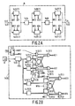
- An embodiment of such a transform circuit is shown diagrammatically in Fig. 2A. This embodiment is based on the expression (3) stated in section A(2).
- the transform circuit 14 has an input 14.01 to which the pixels s(n) are applied and an output 14.02 at which the weighting factors y i,k occur.
- Two picture memories 14.03(1) and 14.03(2) are connected to the input 14.01.
- the address AD1, AD2 applied to the address input of the relevant picture memory determines at which location in the memory a pixel is stored or which pixel is read.
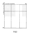
- the picture memory comprises, for example the pixels indicated by dots in Fig. 3.
- the row numbers LN of the picture memory in which visible pixels are written are shown in the vertical direction and the column numbers PN of the picture memory in which visible pixels are written are shown in the horizontal direction.
- NxN pixels 8 in Fig. 3.
- a sub-picture will hereinafter be indicated by X and a pixel thereof by x i,k .
- the pixels of such a sub-picture are applied row by row to a one-dimensional transformer 14.04.
- the sub-picture X is multiplied by the fixed transform matrix A which is also an 8x8 matrix in this case, namely a 8x8 discrete cosine transform matrix (abbreviated DCT matrix).
- the 8x8 product matrix P XA consisting of the elements P i,k is obtained thereby.
- Two sub-picture memories 14.05(.) are connected to the output of this one-dimensional transformer 14.04. Like the picture memories 14.03 (.) they have addressable memory locations and are controlled by write/read commands WR3 and WR4 in such a way that the elements of the product matrix P are written in one of the two memories, whilst the elements of the preceding product matrix P stored in the other memory are read. More particularly the elements P i,k are written row by row in such a memory and read column by column so that the transposed product matrix P T is obtained.
- the address AD3, AD4, which is applied to the address input determines at which location a product element is stored or which product element is read.
- the outputs of the sub-picture memories 14.05(.) are connected to the input of a further one- dimensional transformer 14.06 in which the transposed product matrix P T is multiplied by the said transform matrix A.
- the weighting factors obtained thereby are written in a coefficient memory 14.07(1) or in a coefficient memory 14.07(2).
- control circuit 14.08 shown in Fig. 2B receives clock pulses occurring at a rate f s from a clock pulse generator 8. It is to be noted that these clock pulses are also applied as sampling pulses to the sampling circuit 12 (see Fig. 1). In this control circuit they are applied to a pixel counter 14.10 whose counting position ranges from a zero to a number which is equal to the number of pixels constituting a full picture. This counter is reset at the commencement of each new picture by picture reset pulses FRS which are supplied by the video signal source 3 (Fig. 1).
- the counting positions of this pixel counter are applied as addresses to the address inputs of two memories 14.11(2) each in the form of a ROM. More particularly the ROM 14.11(1) supplies the addresses for the picture memories 14.03(.) in the sequence in which the pixels must be read (read addresses), whilst the ROM 14.11(2) supplies the addresses for the picture memories 14.03(.) in the sequence in which pixels must be written in the picture memory (write addresses).
- the addresses supplied by these ROMs 14.11(.) are applied via AND gate circuits 14.12(.) and OR gate circuits 14.13(.) to the address inputs of the picture memories 14.03(.).
- the picture reset pulses FRS are also applied to a T-flip-flop 14.14. Its Q output supplies the write/read command WR1 and its Q output supplies the write/read command WR2. These commands are applied to the AND gate circuits 14.12(.) in the manner shown.
- the counting positions of pixel counter 14.10 are also applied to two further memories 14.15(.) which are both in the form of ROMs and in which the ROM 14.15(1) supplies NxN read addresses for the memories 14.05(.) and 14.07(.) and the ROM 14.15(2) supplies NxN write addresses.
- a row of pixels of the sub-picture X and a column of product elements of the product matrix P is each time multiplied by the NxN DCT matrix A. Since both multiplications are of the same kind, the multiplication of an array of 1 x N data elements d o to d N-1 by the DCT matrix A will hereinafter be described in general terms. This multiplication will be referred to as transform process. In conformity with the foregoing N will be chosen to be 8. These data elements thus represent, for example the pixels of the i-th row of X. The array of 1 x N product elements obtained by this multiplication will be indicated by P o , ... P N-1 .
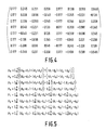
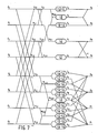
- the absolute value of each element a i,k ofthe discrete cosine transform matrix in expression (6) can be equated to such a transform element if they are defined as follows: (7) ...
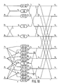
- This diagram comprises a number of combination points which are marked by dots and at which the data elements applied to such a dot are added together or subtracted from one another. In the latter case the digit - -1 is indicated next to a branch terminating at said combination point. Furthermore a plurality of nodes is present from which a given data element is applied via different branches to different combination points.
- the first-order sum elements u l,r and the first-order difference elements v l,r are obtained by performing adding and subtracting operations.
- the first-order sum elements u l,r are converted in a second iteration step into second-order sum elements u 2,r and second-order difference elements v 2,r .
- For the relationship between the q-th-order sum and difference elements which are obtained in the q-th iteration step and the q-1st-order sum elements obtained in the previous iteration step it generally holds that (8a) ... u q,r u q-1,r + u q-1,2 -q+1 N-r-1 (8b) ...
- the difference elements obtained in the q-th iteration step are subjected to a plurality of further iteration steps in which a plurality of auxiliary sum elements is obtained from the difference elements v q,r .
- the auxiliary sum element obtained in the j-th iteration step starting from the elements v q,r is generally denoted by w q,j,m in which m is the ordinal number of the auxiliary sum element in the j-th iteration step.
- w q,j,m In conformity with the foregoing w q,j,m will be referred to as j-th order auxiliary sum element.
- j-th order auxiliary sum element For the relationship between the j-th order and the j-1st order auxiliary sum elements it holds that (9) ...
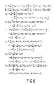
- the sum elements u 2,0 and u 2,1 (generally u Q,0 and u Q,1 ) all difference elements v q,r as well as all auxiliary sum elements w q,j,m are multiplied by a suitably chosen multiplication factor and finally the sub-products obtained thereby are selectively combined with one another. This means that each time certain sub-products are added together or subtracted from one another in order to supply a product element p k .
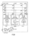
- Fig. 8 shows a one-dimensional DCT transformer 14.04 or 14.06 for performing the new DCT transform shown in Fig. 7. It has an input 14.040 and an output 14.041.
- a data bus 14.042 through which the received data elements d k are transported is connected to the input.
- the bits of these data elements are assumed to be available in parallel so that the said data bus consists of a number of parallel lines corresponding to this number of bits.
- the data buses 14.042, 14.043 and 14.044 can be connected to a column bus 14.046 by means of switching devices SW1, SW2, SW3,
- the databuses 14.042, 14.043, 14.045 can be connected to a column bus 14.047 by means of switching devices SW4, SW5, SW6.
- the data buses 14.042, 14.044, 14.045 can be connected to a column bus 14.048 by means of switching devices SW7, SW8, SW9.
- the data buses 14.043, 14.044, 14.045 can be connected to the output 14.041 via a column bus 14.049 by means of switching devices SW10, SW11, SW12.
- the column buses 14.046 and 14.048 are each connected to the inputs 14.0410, 14.0411 of arithmetic logic units 14.0412 and 14.0413, respectively.
- the column bus 14.047 is connected to the input 14.0414 of a multiplier unit 14.0415.
- the arithmetic logic units 14.0412 and 14.0413 each comprise two register banks R1, R2 and R3, R4, respectively. They comprise, for example 12 registers of 12 bits each and are more particularly constituted by a so-called multiport register bank (see, for example References 8 and 9).
- the registers of these banks are addressable for which purpose each register bank has an address input for the reception of addresses AD5, AD6, AD7, AD8.
- Each register bank has an input which is connected to the input 14.0410 and 14.0411, respectively of the relevant arithmetic logic unit. They have also outputs which are connected to inputs of an adding/subtracting unit A/S(.).
- These units receive via a further input an adding/ subtracting command +/-(.) and supply sum or difference elements which are optionally stored in a register of bank R1 or R2 or in a register of bank R3 or R4.
- Each register bank R1 and R2 has a further output which is connected to the data bus 14.045.
- Each register bank R3 and R4 also has a further output which is connected to the data bus 14.043.
- the multiplier unit 14.0415 is provided with a register bank M1 consisting of, for example, two registers of 12 bits. Its input is connected to the input 14.0414 of this unit and its output is connected to an input of a multiplier 14.0416. The latter receives the multiplication factors shown in Fig. 7 in the desired sequence at a further input.
- the products supplied by this multiplier are stored in a 12-bit register of an output register bank M2 the output of which is connected to the data bus 14.044.
- the said multiplication factors received by the multiplier 14.0416 are supplied by a memory unit 14.0417 with addressable memory locations, for example a ROM. For addressing a memory location this ROM receives an address AD11.
- the registers of the register banks, R1, R2, R3 and R4 the registers of the register banks M1 and M2 are also addressable. To this end they receive the respective addresses AD9 and AD10.
- the transformer is provided with a memory 14.0418 with addressable memory locations, such as a ROM.
- Each memory location comprises a plurality of bits which define the state of all elements to be controlled at a certain moment.
- the state of the switching devices SW the difference addresses, and so forth. It appears in practice that approximately 70 bits per instant may suffice and that not more than 16 of these 70 bits memory locations are required.
- These bits are applied by means of a bus 14.0419 of approximately 70 parallel lines to the different elements of the circuit.
- This ROM is in turn addressedby addresses which are suppliedby a modulo-16-counter 14.0420 which is reset by each FRS pulse generated by the video signal source 3 (see Fig.
- the said clock pulses occur at the sampling frequency f s and are supplied, for example by the clock pulse generator 8 (Fig. 2B).
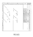
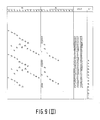
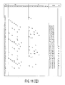
- Fig. 9 The operation of this one-dimensional DCT transformer is shown diagrammatically in Fig. 9 which is self-evident.
- column T indicates the counting positions of the modulo-16-counter.
- the columns denoted by R1, R2, R3, R4, M1, M2 relate to the contents of the different register banks. More particularly the columns r0, r1, ...,indicate the contents of the relevant registers of these register banks.
- the columns denoted by A/S (1) and A/S (2) indicate which quantities at this counting position T of counter 14.0420 are added together or are subtracted from one another in the adding/subtracting units A/S(1) and A/S(2), respectively.
- the column denoted by M2 indicates the sub-product supplied by the multiplier 14.0416 and stored in M2 with the same designation as in Fig. 7.
- the column denoted by OUT indicates the product elements p k occurring at the output 14.041.
- u 1,3 is stored in register r1 of R2 and v 1,3 is stored in register M1 and multiplied by -C516-C316 so that the sub-product z11 is obtained.
- the data element d4 is replaced by d5 in register r0 of R2 and in the adding/subtracting unit A/S(1) d5 is subtracted from d2 resulting in v 1,2 .
- u 1,2 is stored in register r2 of R2, z11 is stored in register r0 of R3, the sub-product z12 is stored in register m0 of M2. Furthermore v 1,2 is stored in register m0 of M1 and multiplied by C716 + C116 resulting in the sub-product z5. Furthermore d6 is stored in register r0 of R2 and d6 is subtracted from d1 so that v 1,1 is obtained. Corresponding operations are performed at the further counting positions of counter 14.0420.
- the decoding station 2 For regaining the original video signal samples the decoding station 2 (see Fig. 1) is provided with an inverse transform circuit 24 which is adapted to perform a two-dimensional inverse discrete cosine transform on an array of NxN basis picture weighting factors y ⁇ i,k which are presented to this circuit.
- An embodiment of such an inverse transform circuit is obtained by inverting the signal direction in the transform circuit shown in Fig. 2 and by forming the two one-dimensional inverse transformers in the way as is shown in Fig. 8 in which the contents of the ROM 14.0418 are chosen to be such that this inverse transformer operates in the desired manner.
Landscapes
- Physics & Mathematics (AREA)
- Engineering & Computer Science (AREA)
- General Physics & Mathematics (AREA)
- Mathematical Physics (AREA)
- Data Mining & Analysis (AREA)
- Mathematical Optimization (AREA)
- Mathematical Analysis (AREA)
- Pure & Applied Mathematics (AREA)
- Computational Mathematics (AREA)
- Theoretical Computer Science (AREA)
- General Engineering & Computer Science (AREA)
- Databases & Information Systems (AREA)
- Software Systems (AREA)
- Algebra (AREA)
- Discrete Mathematics (AREA)
- Multimedia (AREA)
- Signal Processing (AREA)
- Compression Or Coding Systems Of Tv Signals (AREA)
- Complex Calculations (AREA)
- Compression, Expansion, Code Conversion, And Decoders (AREA)
- Two-Way Televisions, Distribution Of Moving Picture Or The Like (AREA)
- Image Processing (AREA)
Priority Applications (1)
| Application Number | Priority Date | Filing Date | Title |
|---|---|---|---|
| AT88200639T ATE77907T1 (de) | 1987-04-10 | 1988-04-06 | Fernsehuebertragungssystem mit verwendung von transformationskodierung. |
Applications Claiming Priority (2)
| Application Number | Priority Date | Filing Date | Title |
|---|---|---|---|
| NL8700843 | 1987-04-10 | ||
| NL8700843A NL8700843A (nl) | 1987-04-10 | 1987-04-10 | Televisie-overdrachtsysteem met transformcoding. |
Publications (2)
| Publication Number | Publication Date |
|---|---|
| EP0286183A1 true EP0286183A1 (fr) | 1988-10-12 |
| EP0286183B1 EP0286183B1 (fr) | 1992-07-01 |
Family
ID=19849837
Family Applications (1)
| Application Number | Title | Priority Date | Filing Date |
|---|---|---|---|
| EP88200639A Expired - Lifetime EP0286183B1 (fr) | 1987-04-10 | 1988-04-06 | Système de transmission de télévision utilisant le codage par transformée |
Country Status (8)
| Country | Link |
|---|---|
| US (1) | US4831440A (fr) |
| EP (1) | EP0286183B1 (fr) |
| JP (1) | JP2630802B2 (fr) |
| KR (1) | KR970004533B1 (fr) |
| CN (1) | CN1009414B (fr) |
| AT (1) | ATE77907T1 (fr) |
| DE (1) | DE3872424T2 (fr) |
| NL (1) | NL8700843A (fr) |
Cited By (4)
| Publication number | Priority date | Publication date | Assignee | Title |
|---|---|---|---|---|
| GB2266208A (en) * | 1992-04-07 | 1993-10-20 | Sony Broadcast & Communication | Image data processing apparatus and method |
| EP0566184A3 (fr) * | 1992-04-13 | 1994-11-17 | Philips Electronics Nv | Transformateur d'image ainsi que système de télévision comportant un émetteur et un récepteur munis d'un transformateur. |
| US5450557A (en) * | 1989-11-07 | 1995-09-12 | Loral Aerospace Corp. | Single-chip self-configurable parallel processor |
| EP0400748B1 (fr) * | 1989-06-02 | 1997-08-20 | STMicroelectronics S.r.l. | Méthode et dispositif pour la computation de transformations bidimensionelles |
Families Citing this family (48)
| Publication number | Priority date | Publication date | Assignee | Title |
|---|---|---|---|---|
| US6336180B1 (en) | 1997-04-30 | 2002-01-01 | Canon Kabushiki Kaisha | Method, apparatus and system for managing virtual memory with virtual-physical mapping |
| EP0576749B1 (fr) * | 1992-06-30 | 1999-06-02 | Discovision Associates | Système de données en pipeline |
| GB9405914D0 (en) * | 1994-03-24 | 1994-05-11 | Discovision Ass | Video decompression |
| FR2626693B1 (fr) * | 1987-12-03 | 1990-08-10 | France Etat | Dispositif et procede a memoire tampon, notamment pour la transposition matricielle ligne-colonne de sequences de donnees |
| NL8801154A (nl) * | 1988-05-03 | 1989-12-01 | Philips Nv | Televisie-overdrachtsysteem met overdracht van basisbeeldgewichtsfaktoren. |
| NL8801207A (nl) * | 1988-05-09 | 1989-12-01 | Philips Nv | Televisie-overdrachtsysteem met differentiele kodering van transformatie coefficienten. |
| US4941043A (en) * | 1988-06-14 | 1990-07-10 | Siemens Aktiengesellschaft | Method for reducing blocking artifacts in video scene coding with discrete cosine transformation (DCT) at a low data rate |
| JP2666411B2 (ja) * | 1988-10-04 | 1997-10-22 | 三菱電機株式会社 | 二次元離散データ直交変換用集積回路装置 |
| JPH02226886A (ja) * | 1989-02-28 | 1990-09-10 | Sony Corp | データ伝送装置及び伝送方法 |
| JPH02249380A (ja) * | 1989-03-22 | 1990-10-05 | Toshiba Corp | 画像記録再生装置 |
| US5008848A (en) * | 1989-05-30 | 1991-04-16 | North American Philips Corporation | Circuit for performing S-transform |
| US5053985A (en) * | 1989-10-19 | 1991-10-01 | Zoran Corporation | Recycling dct/idct integrated circuit apparatus using a single multiplier/accumulator and a single random access memory |
| US5253275A (en) * | 1991-01-07 | 1993-10-12 | H. Lee Browne | Audio and video transmission and receiving system |
| US5649029A (en) * | 1991-03-15 | 1997-07-15 | Galbi; David E. | MPEG audio/video decoder |
| JP2530090B2 (ja) * | 1992-02-28 | 1996-09-04 | 三星電子株式会社 | 映像信号符号化装置 |
| KR0135873B1 (ko) * | 1992-03-14 | 1998-05-15 | 강진구 | 디지탈 자기기록재생방법 및 장치 |
| EP0575675B1 (fr) * | 1992-06-26 | 1998-11-25 | Discovision Associates | Procédé et appareil de transformation de signaux à partir d'un domaine de fréquence dans un domaine du temps |
| US6079009A (en) * | 1992-06-30 | 2000-06-20 | Discovision Associates | Coding standard token in a system compromising a plurality of pipeline stages |
| US5809270A (en) * | 1992-06-30 | 1998-09-15 | Discovision Associates | Inverse quantizer |
| US6435737B1 (en) | 1992-06-30 | 2002-08-20 | Discovision Associates | Data pipeline system and data encoding method |
| US5768561A (en) * | 1992-06-30 | 1998-06-16 | Discovision Associates | Tokens-based adaptive video processing arrangement |
| US6047112A (en) * | 1992-06-30 | 2000-04-04 | Discovision Associates | Technique for initiating processing of a data stream of encoded video information |
| US6330665B1 (en) | 1992-06-30 | 2001-12-11 | Discovision Associates | Video parser |
| US7095783B1 (en) | 1992-06-30 | 2006-08-22 | Discovision Associates | Multistandard video decoder and decompression system for processing encoded bit streams including start codes and methods relating thereto |
| US6067417A (en) * | 1992-06-30 | 2000-05-23 | Discovision Associates | Picture start token |
| US5784631A (en) * | 1992-06-30 | 1998-07-21 | Discovision Associates | Huffman decoder |
| US6112017A (en) * | 1992-06-30 | 2000-08-29 | Discovision Associates | Pipeline processing machine having a plurality of reconfigurable processing stages interconnected by a two-wire interface bus |
| US5339265A (en) * | 1992-08-31 | 1994-08-16 | University Of Maryland At College Park | Optimal unified architectures for the real-time computation of time-recursive discrete sinusoidal transforms |
| US5614952A (en) * | 1994-10-11 | 1997-03-25 | Hitachi America, Ltd. | Digital video decoder for decoding digital high definition and/or digital standard definition television signals |
| US5345408A (en) * | 1993-04-19 | 1994-09-06 | Gi Corporation | Inverse discrete cosine transform processor |
| US5835792A (en) * | 1993-06-24 | 1998-11-10 | Discovision Associates | Token-based adaptive video processing arrangement |
| US5699544A (en) * | 1993-06-24 | 1997-12-16 | Discovision Associates | Method and apparatus for using a fixed width word for addressing variable width data |
| US5861894A (en) * | 1993-06-24 | 1999-01-19 | Discovision Associates | Buffer manager |
| US5805914A (en) * | 1993-06-24 | 1998-09-08 | Discovision Associates | Data pipeline system and data encoding method |
| CA2145365C (fr) * | 1994-03-24 | 1999-04-27 | Anthony M. Jones | Methode d'acces a des batteries de memoires vives dynamiques |
| CA2145363C (fr) * | 1994-03-24 | 1999-07-13 | Anthony Mark Jones | Interface pour memoire vive |
| CA2145379C (fr) * | 1994-03-24 | 1999-06-08 | William P. Robbins | Methode et dispositif d'adressage memoire |
| GB9417138D0 (en) * | 1994-08-23 | 1994-10-12 | Discovision Ass | Data rate conversion |
| JP3058028B2 (ja) * | 1994-10-31 | 2000-07-04 | 三菱電機株式会社 | 画像符号化データ再符号化装置 |
| US6006245A (en) * | 1996-12-20 | 1999-12-21 | Compaq Computer Corporation | Enhanced fast fourier transform technique on vector processor with operand routing and slot-selectable operation |
| AUPO648397A0 (en) | 1997-04-30 | 1997-05-22 | Canon Information Systems Research Australia Pty Ltd | Improvements in multiprocessor architecture operation |
| US6707463B1 (en) | 1997-04-30 | 2004-03-16 | Canon Kabushiki Kaisha | Data normalization technique |
| US6195674B1 (en) | 1997-04-30 | 2001-02-27 | Canon Kabushiki Kaisha | Fast DCT apparatus |
| US6061749A (en) | 1997-04-30 | 2000-05-09 | Canon Kabushiki Kaisha | Transformation of a first dataword received from a FIFO into an input register and subsequent dataword from the FIFO into a normalized output dataword |
| AUPO647997A0 (en) | 1997-04-30 | 1997-05-22 | Canon Information Systems Research Australia Pty Ltd | Memory controller architecture |
| US6414687B1 (en) | 1997-04-30 | 2002-07-02 | Canon Kabushiki Kaisha | Register setting-micro programming system |
| CN100452880C (zh) * | 2006-06-09 | 2009-01-14 | 清华大学 | 一种用于视频编码的整数离散余弦变换方法 |
| CN101106714A (zh) * | 2007-07-29 | 2008-01-16 | 浙江大学 | 应用于视频和图像处理的变换方法 |
Citations (6)
| Publication number | Priority date | Publication date | Assignee | Title |
|---|---|---|---|---|
| US4302775A (en) * | 1978-12-15 | 1981-11-24 | Compression Labs, Inc. | Digital video compression system and methods utilizing scene adaptive coding with rate buffer feedback |
| US4385363A (en) * | 1978-12-15 | 1983-05-24 | Compression Labs, Inc. | Discrete cosine transformer |
| EP0154341A1 (fr) * | 1984-03-09 | 1985-09-11 | Alcatel Cit | Processeur de calcul d'une transformée discrète du cosinus |
| EP0154340A1 (fr) * | 1984-03-09 | 1985-09-11 | Alcatel Cit | Processeur de calcul d'une transformée discrète inverse du cosinus |
| EP0204603A1 (fr) * | 1985-05-22 | 1986-12-10 | Telecom France | Circuit de calcul rapide de la transformée en cosinus, directe ou inverse, d'un signal discret |
| EP0206847A1 (fr) * | 1985-05-03 | 1986-12-30 | Thomson Grand Public | Dispositifs de calcul de transformées cosinus, dispositif de codage et dispositif de décodage d'images comportant de tels dispositifs de calcul |
Family Cites Families (8)
| Publication number | Priority date | Publication date | Assignee | Title |
|---|---|---|---|---|
| US4293920A (en) * | 1979-09-04 | 1981-10-06 | Merola Pasquale A | Two-dimensional transform processor |
| NL8003873A (nl) * | 1980-07-04 | 1982-02-01 | Philips Nv | Werkwijze voor het digitaliseren van een tijd-discreet videosignaal met toepassing van een beeld-transformatie. |
| NL8004521A (nl) * | 1980-08-08 | 1982-03-01 | Philips Nv | Werkwijze voor het digitaliseren van een kleuren-videosignaal. |
| US4449194A (en) * | 1981-09-25 | 1984-05-15 | Motorola Inc. | Multiple point, discrete cosine processor |
| US4491937A (en) * | 1982-02-25 | 1985-01-01 | Trw Inc. | Multiport register file |
| US4554645A (en) * | 1983-03-10 | 1985-11-19 | International Business Machines Corporation | Multi-port register implementation |
| JPS6039988A (ja) * | 1983-08-15 | 1985-03-02 | Nec Corp | 画像信号変換装置 |
| JPS60220466A (ja) * | 1984-04-17 | 1985-11-05 | Fujitsu Ltd | 高速フ−リエ変換装置 |
-
1987
- 1987-04-10 NL NL8700843A patent/NL8700843A/nl not_active Application Discontinuation
-
1988
- 1988-03-24 US US07/172,603 patent/US4831440A/en not_active Expired - Fee Related
- 1988-04-04 JP JP63082872A patent/JP2630802B2/ja not_active Expired - Lifetime
- 1988-04-06 EP EP88200639A patent/EP0286183B1/fr not_active Expired - Lifetime
- 1988-04-06 DE DE8888200639T patent/DE3872424T2/de not_active Expired - Fee Related
- 1988-04-06 AT AT88200639T patent/ATE77907T1/de not_active IP Right Cessation
- 1988-04-07 CN CN88102019A patent/CN1009414B/zh not_active Expired
- 1988-04-09 KR KR88004034A patent/KR970004533B1/ko not_active Expired - Lifetime
Patent Citations (6)
| Publication number | Priority date | Publication date | Assignee | Title |
|---|---|---|---|---|
| US4302775A (en) * | 1978-12-15 | 1981-11-24 | Compression Labs, Inc. | Digital video compression system and methods utilizing scene adaptive coding with rate buffer feedback |
| US4385363A (en) * | 1978-12-15 | 1983-05-24 | Compression Labs, Inc. | Discrete cosine transformer |
| EP0154341A1 (fr) * | 1984-03-09 | 1985-09-11 | Alcatel Cit | Processeur de calcul d'une transformée discrète du cosinus |
| EP0154340A1 (fr) * | 1984-03-09 | 1985-09-11 | Alcatel Cit | Processeur de calcul d'une transformée discrète inverse du cosinus |
| EP0206847A1 (fr) * | 1985-05-03 | 1986-12-30 | Thomson Grand Public | Dispositifs de calcul de transformées cosinus, dispositif de codage et dispositif de décodage d'images comportant de tels dispositifs de calcul |
| EP0204603A1 (fr) * | 1985-05-22 | 1986-12-10 | Telecom France | Circuit de calcul rapide de la transformée en cosinus, directe ou inverse, d'un signal discret |
Non-Patent Citations (2)
| Title |
|---|
| IEEE TRANSACTIONS ON COMPUTERS, vol. c-31, no. 9, September 1982, pages 899-906, IEEE, New York, US; F. KAMANGAR et al.: "Fast algorithms for the 2-D discrete cosine transform" * |
| IEEE TRANSACTIONS ON ELECTROMAGNETIC COMPATIBILITY, vol. EMC-24, no. 2, May 1982, pages 278-286, IEEE, New York, US; A. JALALI et al.: "A high-speed FDCT processor for real-time processing of NTSC color TV signal" * |
Cited By (6)
| Publication number | Priority date | Publication date | Assignee | Title |
|---|---|---|---|---|
| EP0400748B1 (fr) * | 1989-06-02 | 1997-08-20 | STMicroelectronics S.r.l. | Méthode et dispositif pour la computation de transformations bidimensionelles |
| US5450557A (en) * | 1989-11-07 | 1995-09-12 | Loral Aerospace Corp. | Single-chip self-configurable parallel processor |
| GB2266208A (en) * | 1992-04-07 | 1993-10-20 | Sony Broadcast & Communication | Image data processing apparatus and method |
| US5450506A (en) * | 1992-04-07 | 1995-09-12 | Sony United Kingdom, Ltd. | Image data processing apparatus and method |
| GB2266208B (en) * | 1992-04-07 | 1995-10-11 | Sony Broadcast & Communication | Image data processing apparatus and method |
| EP0566184A3 (fr) * | 1992-04-13 | 1994-11-17 | Philips Electronics Nv | Transformateur d'image ainsi que système de télévision comportant un émetteur et un récepteur munis d'un transformateur. |
Also Published As
| Publication number | Publication date |
|---|---|
| CN1009414B (zh) | 1990-08-29 |
| US4831440A (en) | 1989-05-16 |
| NL8700843A (nl) | 1988-11-01 |
| EP0286183B1 (fr) | 1992-07-01 |
| JPS6419887A (en) | 1989-01-23 |
| DE3872424T2 (de) | 1993-02-18 |
| KR880013400A (ko) | 1988-11-30 |
| JP2630802B2 (ja) | 1997-07-16 |
| ATE77907T1 (de) | 1992-07-15 |
| KR970004533B1 (en) | 1997-03-28 |
| CN88102019A (zh) | 1988-12-21 |
| DE3872424D1 (de) | 1992-08-06 |
Similar Documents
| Publication | Publication Date | Title |
|---|---|---|
| EP0286183B1 (fr) | Système de transmission de télévision utilisant le codage par transformée | |
| US4912668A (en) | Mono-dimensional reverse cosine transform computing device | |
| US5345408A (en) | Inverse discrete cosine transform processor | |
| US5999957A (en) | Lossless transform coding system for digital signals | |
| US5539836A (en) | Method and apparatus for the realization of two-dimensional discrete cosine transform for an 8*8 image fragment | |
| US5815421A (en) | Method for transposing a two-dimensional array | |
| EP0353223B1 (fr) | Processeur permettant d'obtenir des transformees de cosinus discretes bidimensionnelles | |
| US5325215A (en) | Matrix multiplier and picture transforming coder using the same | |
| EP0286184B1 (fr) | Transformateur d'images linéaire unidimensionnel | |
| US5331585A (en) | Orthogonal transformation processor for compressing information | |
| US5649077A (en) | Modularized architecture for rendering scaled discrete cosine transform coefficients and inverse thereof for rapid implementation | |
| EP0013069A1 (fr) | Processeur et méthode de traitement d'information vidéo | |
| EP0245903A1 (fr) | Système de calcul d'une transformée discrète du cosinus | |
| US6421695B1 (en) | Apparatus for implementing inverse discrete cosine transform in digital image processing system | |
| US5757432A (en) | Manipulating video and audio signals using a processor which supports SIMD instructions | |
| US5528528A (en) | Method, apparatus, and system for transforming signals | |
| US4814871A (en) | Method for the transmission of a video signal | |
| US5995990A (en) | Integrated circuit discrete integral transform implementation | |
| US5291429A (en) | Circuit for matrix calculation of discrete cosine transformation | |
| EP0566184A2 (fr) | Transformateur d'image ainsi que système de télévision comportant un émetteur et un récepteur munis d'un transformateur | |
| US4860097A (en) | Transformation circuit | |
| US5555321A (en) | Image data binary coding method and apparatus | |
| EP0836322B1 (fr) | Dispositif de codage d'images utilisant un système de traitement analogique | |
| US6111989A (en) | 1/4 size real time decoding of digital video | |
| JP2946612B2 (ja) | Idct処理装置 |
Legal Events
| Date | Code | Title | Description |
|---|---|---|---|
| PUAI | Public reference made under article 153(3) epc to a published international application that has entered the european phase |
Free format text: ORIGINAL CODE: 0009012 |
|
| AK | Designated contracting states |
Kind code of ref document: A1 Designated state(s): AT DE FR GB IT |
|
| 17P | Request for examination filed |
Effective date: 19890407 |
|
| 17Q | First examination report despatched |
Effective date: 19910708 |
|
| GRAA | (expected) grant |
Free format text: ORIGINAL CODE: 0009210 |
|
| AK | Designated contracting states |
Kind code of ref document: B1 Designated state(s): AT DE FR GB IT |
|
| REF | Corresponds to: |
Ref document number: 77907 Country of ref document: AT Date of ref document: 19920715 Kind code of ref document: T |
|
| REF | Corresponds to: |
Ref document number: 3872424 Country of ref document: DE Date of ref document: 19920806 |
|
| ITF | It: translation for a ep patent filed | ||
| ET | Fr: translation filed | ||
| ITTA | It: last paid annual fee | ||
| PLBE | No opposition filed within time limit |
Free format text: ORIGINAL CODE: 0009261 |
|
| STAA | Information on the status of an ep patent application or granted ep patent |
Free format text: STATUS: NO OPPOSITION FILED WITHIN TIME LIMIT |
|
| 26N | No opposition filed | ||
| ITPR | It: changes in ownership of a european patent |
Owner name: CAMBIO RAGIONE SOCIALE;PHILIPS ELECTRONICS N.V. |
|
| REG | Reference to a national code |
Ref country code: FR Ref legal event code: CD |
|
| PGFP | Annual fee paid to national office [announced via postgrant information from national office to epo] |
Ref country code: GB Payment date: 19960329 Year of fee payment: 9 |
|
| PGFP | Annual fee paid to national office [announced via postgrant information from national office to epo] |
Ref country code: AT Payment date: 19960424 Year of fee payment: 9 |
|
| PGFP | Annual fee paid to national office [announced via postgrant information from national office to epo] |
Ref country code: FR Payment date: 19960429 Year of fee payment: 9 |
|
| PGFP | Annual fee paid to national office [announced via postgrant information from national office to epo] |
Ref country code: DE Payment date: 19960625 Year of fee payment: 9 |
|
| PG25 | Lapsed in a contracting state [announced via postgrant information from national office to epo] |
Ref country code: GB Effective date: 19970406 Ref country code: AT Effective date: 19970406 |
|
| GBPC | Gb: european patent ceased through non-payment of renewal fee |
Effective date: 19970406 |
|
| PG25 | Lapsed in a contracting state [announced via postgrant information from national office to epo] |
Ref country code: FR Free format text: LAPSE BECAUSE OF NON-PAYMENT OF DUE FEES Effective date: 19971231 |
|
| PG25 | Lapsed in a contracting state [announced via postgrant information from national office to epo] |
Ref country code: DE Free format text: LAPSE BECAUSE OF NON-PAYMENT OF DUE FEES Effective date: 19980101 |
|
| REG | Reference to a national code |
Ref country code: FR Ref legal event code: ST |
|
| PG25 | Lapsed in a contracting state [announced via postgrant information from national office to epo] |
Ref country code: IT Free format text: LAPSE BECAUSE OF NON-PAYMENT OF DUE FEES;WARNING: LAPSES OF ITALIAN PATENTS WITH EFFECTIVE DATE BEFORE 2007 MAY HAVE OCCURRED AT ANY TIME BEFORE 2007. THE CORRECT EFFECTIVE DATE MAY BE DIFFERENT FROM THE ONE RECORDED. Effective date: 20050406 |