EP0286390A2 - Amplificateur micro-ondes à FET à combinaison de puissance - Google Patents
Amplificateur micro-ondes à FET à combinaison de puissance Download PDFInfo
- Publication number
- EP0286390A2 EP0286390A2 EP88303080A EP88303080A EP0286390A2 EP 0286390 A2 EP0286390 A2 EP 0286390A2 EP 88303080 A EP88303080 A EP 88303080A EP 88303080 A EP88303080 A EP 88303080A EP 0286390 A2 EP0286390 A2 EP 0286390A2
- Authority
- EP
- European Patent Office
- Prior art keywords
- fet
- circuit
- power combining
- microwave power
- fets
- Prior art date
- Legal status (The legal status is an assumption and is not a legal conclusion. Google has not performed a legal analysis and makes no representation as to the accuracy of the status listed.)
- Granted
Links
Images

Classifications
-
- H—ELECTRICITY
- H03—ELECTRONIC CIRCUITRY
- H03F—AMPLIFIERS
- H03F3/00—Amplifiers with only discharge tubes or only semiconductor devices as amplifying elements
- H03F3/60—Amplifiers in which coupling networks have distributed constants, e.g. with waveguide resonators
- H03F3/602—Combinations of several amplifiers
- H03F3/604—Combinations of several amplifiers using FET's
Definitions
- the present invention relates to a microwave power combining FET amplifier for amplifyinq and combining power of microwave by using a microwave integrated circuit.
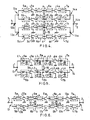
- Fig.1 is a circuit diagram of a prior art microwave power combining FET amplifier shown, for example, in the above-mentioned 1984 IEEE MTT-S Digest, pp 227 ⁇ 228, " A 1.5 Watt 28 GHz Band FET Amplifier".
- numeral 1 designates an input terminal, 2 an output terminal, 3a and 3b pre-stage FETs, 4a and 4b post-stage FETs, 5a and 5b input matching circuits, 6a and 6b interstage matching circuits, 7a and 7b output matching circuits, 8 a power splitter, and 9 a power combiner.
- the power splitter 8 and power combiner 9 in Fig.1 use branch-line type couplers or Wilkinson type couplers.
- the microwave power inputted from the input terminal 1 is split by the power splitter 8, and one of the split microwave power is supplied to the power combiner 9 through the input matching circuit 5a, pre-stage FET 3a, interstage matching circuit 6a, post-stage FET 4a, and output matching circuit 7a.
- the other of the split microwave power is also suplied to the power combiner 9 through the input matching circuit 5b, pre-stage FET 3b, interstage matching circuit 6b, post-stage FET 4b, and output matching circuit 7b.
- the split two microwave powers are matched respectively by the input matching circuits 5a, 5b, interstage matching circuits 6a, 6b, and output matching circuits 7a, 7b, and at the same time amplified by the FETs 3a, 3b, 4a, and 4b.
- the two microwave powers supplied to the power combiner 9 are combined, and amplified and combined microwave power is outputted from the output terminal 2.
- the power splitter 8 and power combiner 9 have in the inside thereof resistance circuits for isolation, and the resistance circuits for isolation serve to absorb the microwave power which propagates in a propagation mode of odd mode due to microwaves having equal amplitude and oppsite phases caused by non-uniformity of characteristics of individual FETs 3a, 3b, 4a, and 4b.
- the amplifier arranged as shown in Fig.1 can be operated stably.
- the present invention was made to solve the above problem, and it is an object of the invention to provide a microwave power combining FET amplifier without including a power splitting circuit and a power combining circuit which employ a branch-line type coupler or a Wilkinson type coupler, and yet performing equivalent function to these circuits thereby enabling to arrange in a simple structure and in a small size.
- the above object is realized by providing a microwave power combining FET amplifier which comprises T-type branch circuits for power splitting and for power combining, a plurality of multistage FETs, interstage matching circuits provided respectively corresponding to the multistage FETs, and a resistance circuit having a predetermined resistance value connected between predetermined opposing positions of the interstage matching circuits.
- Fig.2 is a circuit diagram of a microwave power combining FET amplifier according to a first embodiment of the invention.
- identical reference numerals are used to refer to corresponding elements in Fig.1, and descriptions thereof are omitted.
- input matching circuits 5a and 5b are constituted by distributed constant transmission lines 16a and 16b respectively, and interstage matching circuits 6a and 6b are respectively constituted by pairs of distributed constant transmission lines 17a, 18a, and 17b, 18b. Furthermore, output matching circuits 7a and 7b are constituted by distributed constant transmission lines 19a and 19b. Between an input terminal 1 and the input matching circuits 5a, 5b, there is provided with a T-type branch circuit 13 for performing power splitting, and a T-type branch circuit 14 is provided between an output terminal 2 and the output matching circuits 7a, 7b for performing power combining.
- the interstage matching circuits 6a and 6b are provided respectively correspondinq to a plurality of FETs (multi-stage FET amplifier) 3a and 4a and a plurality of FETs 3b and 4b, and a resistance circuit 15 having a predetermined resistance value is connected between predetermined positions a and b opposing to each other and respectively in the interstage matching circuits 6a and 6b.
- the distimped constant transmission lines 16a, 16b, 17a, 17b, 18a, 18b, 19a, and 19b are formed by microstrip lines ( line having a single conductor strip disposed in parallel and close to a flat metalic plate).
- the microwave power inputted from the input terminal 1 is split by the T-type branch circuit 13.
- One of the split microwave power is supplied to the T-type branch circuit 14 through the input matching circuit 5a, pre-stage FET 3a, interstage matching circuit 6a, post-stage FET 4a, and output matching circuit 7a.
- the other of the split microwave power is supplied to the T-type branch dircuit 14 through the input matching circuit 5b, pre-stage FET 3b, interstage metching circuit 6b, post-stage FET 4b, and output matching circuit 7b.
- Both the microwave powers split by the T-type branch circuit 13 are respectively amplified by the FETs 3a and 4a and the FETs 3b and 4b, and are combined by the T-type branch circuit 14. Accodingly, the amplified and power combined microwave power is outputted.
- the amplitudes and phases of the two microwaves which reach the T-type branch circuit 14 differ from each other.
- there are two types of transmission modes of wave that is, an odd mode in which the amplitudes of two waves are equal and the phases are opposite to each, and an even mode in which the amplitudes and phases of the two waves are equal to each other.
- Two input microwaves having the same amplitude and phase and propagating in the even propagation mode are combined in the T-type branch circuit 14 and delivered to the output terminal 2.
- two input microwaves having the same amplitude and opposite phases and propagating in the odd propagation mode are reflected at the T-type branch circuit 14.
- predetermined positions a and b opposing to each other respectively at the interstage matching circuits 6a and 6b are connected by a resistance circuit 15 to each other to eliminate the influence of the above-mentioned multiple reflection.
- FETs having a large gate width and a high output level are used in the post-stage FETs 4a and 4b as compared with the pre-stage FETs 3a and 3b.
- the FETs having a large gate width are apt to exhibit large non-uniformities in the characteristic of the FETs, the non-uniformities in the characteristic tend to become large in the post-stage FETs 4a and 4b as compared with the pre-stage FETs 3a and 3b.
- the pre-stage FETs 3a and 3b have no non-uniformities in the characteristic therebetween, and the post-stage FETs 4a and 4b have non-uniformities in the characteristic therebetween.
- Fig.3 is a circuit diagram for explaining the principles of operation when the non-uniformities in the characteristic are present in only the post-stage FETs 4a and 4b.
- distributed constant transmission lines 21a and 21b represent the pre-stage FETs 3a and 3b by regarding them approximataely as lines.
- ⁇ 1 and ⁇ 3 are respectively electrical angles due to the distributed constant transmission lines 16a, 16b, and the distributed constant transmission lines 17a and 17b
- ⁇ 2 is an electrical angle which is given by the relationship ⁇ 2 + ⁇ ⁇ S 12 ⁇ ⁇ S 21 among S parameters of the pre-stage FETs 3a and 3b.
- S12 and S21 are elements S12 , and S21 of a so-called Further, Za and Zb are impedances as viewed the sides of the post-stage FETs 4a and 4b from the points a and b.
- Numeral 15 designates a resistance circuit having an impedance Z.
- Za* and Zb* in the formula (2) represent conjugate complexes of Za and Zb.
- the circuit of Fig.3 can be regarded approximately as being equivalent to the Wilkinson type coupler. Accordingly, the microwave power having the same amplitude and opposite phases reflected due to the non-uniformities in the characteristic of the post-FETs 4a and 4b is consumed by the resistance circuit 15 according to the principles of operation similar to that of the Wilkinson type coupler.
- the microwave power split by the T-type branch circuit 13 reaches the T-type branch circuit 14, it is reflected with the same amplitude and opposite phases towards the input side, and due to this reflection, a potential difference is developed across the resistance circuit 15, and the reflected microwave power is fed to the resistance circuit 15 and consumed therein.
- the resistance circuit 15 does not affect the propagation mode in the even mode which contributes to the amplification characteristic, and the resistance circuit 15 functions as an absorbing circuit for the microwave power propagating in the propagation mode of the odd mode which is a cause of the multiple reflection.
- the power splitter and power combiner using the branch-type or Wilkinson type couples employed in the prior art amplifiers of this kind are not particulary necessary, and the structure can be simplified and the shape can be made small in size.
- Fig.4 is a circuit diagram showing a second embodiment of the present invention. ln the second embodiment, four multistage FET amplifiers are used, and corresponding constituent parts to that shown in Fig.2 are designated with identical reference numerals.
- numerals 3c and 3d designate pre-stage FETs, 4c and 4d post-stage FETs, 5c and 5d input matching circuits, 6c and 6d interstage matching circuits, 7c and 7d output matching circuits, and 13a, 13b, 13c, 14a, 14b, and 14c designate T-type branch cirvuits.
- the operation in this second embdiment is the same as the first embodiment, and the description thereof is omitted.
- three or five multistage FET amplifiers or more may be used.
- Fig.5 is a curcuit diagram showing a third embodiment.
- the characteristic features in the third embodiment reside in that each of input matching circuits 5a and 5b is formed by a coil L1 and a capacitor CI, each of interstage matching circuits 6a and 6b is formed by coils L2, L3, and capacitors C2, C3, and each of output matching circuits 7a and 7b is formed by a coil L4 and a capacitor C4.
- the input matching circuits 5a and 5b, interstage matching circuits 6a and 6b, and output matching circuits 7a and 7b are formed by concentrated constant circuit elements.
- the same operation can be performed as in the first embodiment.
- Fig.6 is a circuit diagram showinq a fourth embodiment of the present invention.
- the constituent elements corresponding to that in Fig.2 are designated by identical reference numerals and the description thereof is omitted.
- numerals 10a and 10b designate respectively pre-stage FETs
- 11a and 11b designate intermediate stage FETs
- 12a and 12b designate post-stage FETs.
- the operation is the same as in the first embodiment.
- This embodiment may be formed by four stage or more FETs.
- the present invention may be applied to a monolithic integrared circuit, and a plurality of FETs, input matching circuits, output matching circuits, interstage metching circuits, T-type branch circuits, and resiatance circuits may be formed on the same semiconductor substrate.
Landscapes
- Engineering & Computer Science (AREA)
- Power Engineering (AREA)
- Microwave Amplifiers (AREA)
- Amplifiers (AREA)
Applications Claiming Priority (2)
| Application Number | Priority Date | Filing Date | Title |
|---|---|---|---|
| JP87954/87 | 1987-04-10 | ||
| JP62087954A JPH0767057B2 (ja) | 1987-04-10 | 1987-04-10 | マイクロ波電力合成fet増幅器 |
Publications (3)
| Publication Number | Publication Date |
|---|---|
| EP0286390A2 true EP0286390A2 (fr) | 1988-10-12 |
| EP0286390A3 EP0286390A3 (en) | 1989-07-19 |
| EP0286390B1 EP0286390B1 (fr) | 1993-10-20 |
Family
ID=13929269
Family Applications (1)
| Application Number | Title | Priority Date | Filing Date |
|---|---|---|---|
| EP88303080A Expired - Lifetime EP0286390B1 (fr) | 1987-04-10 | 1988-04-06 | Amplificateur micro-ondes à FET à combinaison de puissance |
Country Status (3)
| Country | Link |
|---|---|
| US (1) | US4803443A (fr) |
| EP (1) | EP0286390B1 (fr) |
| JP (1) | JPH0767057B2 (fr) |
Cited By (3)
| Publication number | Priority date | Publication date | Assignee | Title |
|---|---|---|---|---|
| WO1992022937A1 (fr) * | 1991-06-14 | 1992-12-23 | Cambridge Computer Limited | Commutateur a isolation eleveee |
| EP1209756A1 (fr) * | 2000-11-28 | 2002-05-29 | Telefonaktiebolaget L M Ericsson (Publ) | Circuit amplificateur de fréquence radio |
| WO2002045206A1 (fr) * | 2000-11-28 | 2002-06-06 | Telefonaktiebolaget Lm Ericsson (Publ) | Circuit d'amplification haute frequence |
Families Citing this family (23)
| Publication number | Priority date | Publication date | Assignee | Title |
|---|---|---|---|---|
| US4959873A (en) * | 1988-07-08 | 1990-09-25 | The Marconi Company Limited | Transmission line switch |
| US4916410A (en) * | 1989-05-01 | 1990-04-10 | E-Systems, Inc. | Hybrid-balun for splitting/combining RF power |
| JPH0785528B2 (ja) * | 1989-12-25 | 1995-09-13 | 日本電気株式会社 | 高出力マイクロ波ミリ波トランジスタ安定化回路 |
| JPH03250807A (ja) * | 1990-02-27 | 1991-11-08 | Mitsubishi Electric Corp | 電力合成形多段増幅器 |
| US5276406A (en) * | 1992-02-13 | 1994-01-04 | Trontech, Inc. | Low noise wide dynamic range amplifiers |
| US5420541A (en) * | 1993-06-04 | 1995-05-30 | Raytheon Company | Microwave doherty amplifier |
| US5543751A (en) * | 1995-07-21 | 1996-08-06 | Motorola, Inc. | Power combiner for use in a radio frequency system and a method of constructing a power combiner |
| JPH0964758A (ja) * | 1995-08-30 | 1997-03-07 | Matsushita Electric Ind Co Ltd | ディジタル携帯無線機の送信装置とそれに用いる高周波電力増幅装置 |
| US5659267A (en) * | 1995-11-03 | 1997-08-19 | Motorola, Inc. | High gain K-band power amplifier with unconditionally stable MMIC FET cells |
| JP3336868B2 (ja) * | 1996-08-09 | 2002-10-21 | 株式会社村田製作所 | 周波数の異なる複数の信号に整合する高周波増幅器 |
| JPH10163772A (ja) * | 1996-10-04 | 1998-06-19 | Sanyo Electric Co Ltd | 電力増幅器およびチップキャリヤ |
| JPH10322147A (ja) * | 1996-10-04 | 1998-12-04 | Toshiba Corp | 高周波電力増幅器およびこれを用いた移動体通信装置 |
| JP3060981B2 (ja) * | 1997-02-21 | 2000-07-10 | 日本電気株式会社 | マイクロ波増幅器 |
| US6486749B1 (en) | 2000-05-05 | 2002-11-26 | Ophir Rf, Inc. | Four-way power combiner/splitter |
| US6954623B2 (en) * | 2003-03-18 | 2005-10-11 | Skyworks Solutions, Inc. | Load variation tolerant radio frequency (RF) amplifier |
| US7268627B2 (en) * | 2004-11-03 | 2007-09-11 | Theta Microelectronics, Inc. | Pre-matching of distributed and push-pull power transistors |
| JP4757530B2 (ja) * | 2005-04-28 | 2011-08-24 | 三菱電機株式会社 | 高周波増幅器 |
| JP5065667B2 (ja) * | 2006-12-22 | 2012-11-07 | 株式会社東芝 | 高周波電力増幅器 |
| US8592966B2 (en) * | 2007-06-22 | 2013-11-26 | Cree, Inc. | RF transistor packages with internal stability network including intra-capacitor resistors and methods of forming RF transistor packages with internal stability networks including intra-capacitor resistors |
| US7876160B2 (en) * | 2008-02-04 | 2011-01-25 | Skyworks Solutions, Inc. | Multi-mode high efficiency linear power amplifier |
| US8634789B2 (en) | 2011-11-10 | 2014-01-21 | Skyworks Solutions, Inc. | Multi-mode power amplifier |
| CN106356597B (zh) * | 2016-09-08 | 2020-07-28 | 复旦大学 | 一种带有耗散管的有源合成器电路 |
| CN115642887A (zh) * | 2022-11-02 | 2023-01-24 | 武汉大学 | 一种矩阵式功率合成毫米波放大器 |
Family Cites Families (4)
| Publication number | Priority date | Publication date | Assignee | Title |
|---|---|---|---|---|
| US3963993A (en) * | 1975-01-31 | 1976-06-15 | The Bendix Corporation | Power amplifier using a plurality of parallel connected amplifier elements and having burn-out protection |
| JPS5443662A (en) * | 1977-09-14 | 1979-04-06 | Nec Corp | Transistor amplifier |
| JPS5455349A (en) * | 1977-10-13 | 1979-05-02 | Nec Corp | Transistor amplifier |
| DE3324540C2 (de) * | 1983-07-07 | 1986-08-28 | Siemens AG, 1000 Berlin und 8000 München | Breitbandiger Mikrowellenverstärker |
-
1987
- 1987-04-10 JP JP62087954A patent/JPH0767057B2/ja not_active Expired - Lifetime
-
1988
- 1988-04-05 US US07/177,738 patent/US4803443A/en not_active Expired - Fee Related
- 1988-04-06 EP EP88303080A patent/EP0286390B1/fr not_active Expired - Lifetime
Cited By (4)
| Publication number | Priority date | Publication date | Assignee | Title |
|---|---|---|---|---|
| WO1992022937A1 (fr) * | 1991-06-14 | 1992-12-23 | Cambridge Computer Limited | Commutateur a isolation eleveee |
| EP1209756A1 (fr) * | 2000-11-28 | 2002-05-29 | Telefonaktiebolaget L M Ericsson (Publ) | Circuit amplificateur de fréquence radio |
| WO2002045206A1 (fr) * | 2000-11-28 | 2002-06-06 | Telefonaktiebolaget Lm Ericsson (Publ) | Circuit d'amplification haute frequence |
| US6794953B2 (en) | 2000-11-28 | 2004-09-21 | Telefonaktiebolaget Lm Ericsson (Publ) | Radio frequency amplifying circuit |
Also Published As
| Publication number | Publication date |
|---|---|
| US4803443A (en) | 1989-02-07 |
| EP0286390B1 (fr) | 1993-10-20 |
| JPS63253708A (ja) | 1988-10-20 |
| EP0286390A3 (en) | 1989-07-19 |
| JPH0767057B2 (ja) | 1995-07-19 |
Similar Documents
| Publication | Publication Date | Title |
|---|---|---|
| EP0286390B1 (fr) | Amplificateur micro-ondes à FET à combinaison de puissance | |
| CA2065199C (fr) | Diviseur-combinateur polyphase | |
| US9362602B2 (en) | Power dividing and/or power-combining circuits with isolation | |
| US4994755A (en) | Active balun | |
| US6236272B1 (en) | Traveling wave power combiner and radio base station | |
| EP1331689A1 (fr) | Circuit diviseur/combineur de puissance | |
| US4668920A (en) | Power divider/combiner circuit | |
| US6621374B2 (en) | Splitter/combiner using artificial transmission lines, and paralleled amplifier using same | |
| US20230261622A1 (en) | Power amplifier circuit | |
| US3789314A (en) | Amplifier utilizing input signal power | |
| JPH11330813A (ja) | 電力分配回路および電力増幅器 | |
| US9000865B2 (en) | Power dividing and power combining circuits | |
| US12456954B2 (en) | High-frequency amplifier, radio communication device, and radar device | |
| US5821815A (en) | Miniature active conversion between slotline and coplanar waveguide | |
| US4760350A (en) | Internally matched power amplifier | |
| US4635005A (en) | Quadrupole for matching of a reactance, independently of the operating frequency | |
| EP0383311B1 (fr) | Amplificateur de puissance à micro-ondes utilisant des inverseurs de phase | |
| Sanada et al. | A waveguide type power divider/combiner of double-ladder multiple-port structure | |
| US5053719A (en) | Wide-band push-pull amplifier | |
| US5008633A (en) | Cross-fed FET power-chip | |
| JPH03250807A (ja) | 電力合成形多段増幅器 | |
| EP0176331A2 (fr) | Circuit de combinaison ou de distribution de signaux | |
| US4424495A (en) | Radio power distributor and radio equipment using such a distributor, particularly in the solid state | |
| CA1079822A (fr) | Amplificateur a jonction hybride a ondes progressives | |
| US4455536A (en) | Push-pull microwave amplifier |
Legal Events
| Date | Code | Title | Description |
|---|---|---|---|
| PUAI | Public reference made under article 153(3) epc to a published international application that has entered the european phase |
Free format text: ORIGINAL CODE: 0009012 |
|
| AK | Designated contracting states |
Kind code of ref document: A2 Designated state(s): FR GB |
|
| PUAL | Search report despatched |
Free format text: ORIGINAL CODE: 0009013 |
|
| AK | Designated contracting states |
Kind code of ref document: A3 Designated state(s): FR GB |
|
| 17P | Request for examination filed |
Effective date: 19890927 |
|
| 17Q | First examination report despatched |
Effective date: 19911126 |
|
| GRAA | (expected) grant |
Free format text: ORIGINAL CODE: 0009210 |
|
| AK | Designated contracting states |
Kind code of ref document: B1 Designated state(s): FR GB |
|
| ET | Fr: translation filed | ||
| REG | Reference to a national code |
Ref country code: GB Ref legal event code: 727 |
|
| REG | Reference to a national code |
Ref country code: GB Ref legal event code: 727A |
|
| REG | Reference to a national code |
Ref country code: GB Ref legal event code: 727A |
|
| REG | Reference to a national code |
Ref country code: GB Ref legal event code: 727B |
|
| PLBE | No opposition filed within time limit |
Free format text: ORIGINAL CODE: 0009261 |
|
| STAA | Information on the status of an ep patent application or granted ep patent |
Free format text: STATUS: NO OPPOSITION FILED WITHIN TIME LIMIT |
|
| 26N | No opposition filed | ||
| REG | Reference to a national code |
Ref country code: GB Ref legal event code: SP |
|
| PGFP | Annual fee paid to national office [announced via postgrant information from national office to epo] |
Ref country code: GB Payment date: 19960328 Year of fee payment: 9 |
|
| PGFP | Annual fee paid to national office [announced via postgrant information from national office to epo] |
Ref country code: FR Payment date: 19960410 Year of fee payment: 9 |
|
| PG25 | Lapsed in a contracting state [announced via postgrant information from national office to epo] |
Ref country code: GB Effective date: 19970406 |
|
| GBPC | Gb: european patent ceased through non-payment of renewal fee |
Effective date: 19970406 |
|
| PG25 | Lapsed in a contracting state [announced via postgrant information from national office to epo] |
Ref country code: FR Free format text: LAPSE BECAUSE OF NON-PAYMENT OF DUE FEES Effective date: 19971231 |
|
| REG | Reference to a national code |
Ref country code: FR Ref legal event code: ST |