EP0286414A2 - Appareil de traitement d'images en couleurs - Google Patents
Appareil de traitement d'images en couleurs Download PDFInfo
- Publication number
- EP0286414A2 EP0286414A2 EP88303136A EP88303136A EP0286414A2 EP 0286414 A2 EP0286414 A2 EP 0286414A2 EP 88303136 A EP88303136 A EP 88303136A EP 88303136 A EP88303136 A EP 88303136A EP 0286414 A2 EP0286414 A2 EP 0286414A2
- Authority
- EP
- European Patent Office
- Prior art keywords
- image
- signal
- color
- processing
- input
- Prior art date
- Legal status (The legal status is an assumption and is not a legal conclusion. Google has not performed a legal analysis and makes no representation as to the accuracy of the status listed.)
- Withdrawn
Links
Images


Classifications
-
- H—ELECTRICITY
- H04—ELECTRIC COMMUNICATION TECHNIQUE
- H04N—PICTORIAL COMMUNICATION, e.g. TELEVISION
- H04N1/00—Scanning, transmission or reproduction of documents or the like, e.g. facsimile transmission; Details thereof
- H04N1/04—Scanning arrangements, i.e. arrangements for the displacement of active reading or reproducing elements relative to the original or reproducing medium, or vice versa
- H04N1/19—Scanning arrangements, i.e. arrangements for the displacement of active reading or reproducing elements relative to the original or reproducing medium, or vice versa using multi-element arrays
- H04N1/195—Scanning arrangements, i.e. arrangements for the displacement of active reading or reproducing elements relative to the original or reproducing medium, or vice versa using multi-element arrays the array comprising a two-dimensional [2D] array
- H04N1/19505—Scanning picture elements spaced apart from one another in at least one direction
- H04N1/19515—Scanning picture elements spaced apart from one another in at least one direction in two directions
-
- H—ELECTRICITY
- H04—ELECTRIC COMMUNICATION TECHNIQUE
- H04N—PICTORIAL COMMUNICATION, e.g. TELEVISION
- H04N1/00—Scanning, transmission or reproduction of documents or the like, e.g. facsimile transmission; Details thereof
- H04N1/04—Scanning arrangements, i.e. arrangements for the displacement of active reading or reproducing elements relative to the original or reproducing medium, or vice versa
- H04N1/19—Scanning arrangements, i.e. arrangements for the displacement of active reading or reproducing elements relative to the original or reproducing medium, or vice versa using multi-element arrays
- H04N1/195—Scanning arrangements, i.e. arrangements for the displacement of active reading or reproducing elements relative to the original or reproducing medium, or vice versa using multi-element arrays the array comprising a two-dimensional [2D] array
- H04N1/19505—Scanning picture elements spaced apart from one another in at least one direction
-
- H—ELECTRICITY
- H04—ELECTRIC COMMUNICATION TECHNIQUE
- H04N—PICTORIAL COMMUNICATION, e.g. TELEVISION
- H04N1/00—Scanning, transmission or reproduction of documents or the like, e.g. facsimile transmission; Details thereof
- H04N1/40—Picture signal circuits
- H04N1/40062—Discrimination between different image types, e.g. two-tone, continuous tone
-
- H—ELECTRICITY
- H04—ELECTRIC COMMUNICATION TECHNIQUE
- H04N—PICTORIAL COMMUNICATION, e.g. TELEVISION
- H04N1/00—Scanning, transmission or reproduction of documents or the like, e.g. facsimile transmission; Details thereof
- H04N1/40—Picture signal circuits
- H04N1/401—Compensating positionally unequal response of the pick-up or reproducing head
-
- H—ELECTRICITY
- H04—ELECTRIC COMMUNICATION TECHNIQUE
- H04N—PICTORIAL COMMUNICATION, e.g. TELEVISION
- H04N1/00—Scanning, transmission or reproduction of documents or the like, e.g. facsimile transmission; Details thereof
- H04N1/46—Colour picture communication systems
- H04N1/56—Processing of colour picture signals
- H04N1/60—Colour correction or control
- H04N1/6016—Conversion to subtractive colour signals
- H04N1/6022—Generating a fourth subtractive colour signal, e.g. under colour removal, black masking
- H04N1/6025—Generating a fourth subtractive colour signal, e.g. under colour removal, black masking using look-up tables
Definitions
- the present invention relates to an image information processing apparatus and, more particularly, to an image signal processing apparatus for processing an input image signal obtained by reading an image pattern such as a paper document using a combination of a plurality of image sensors.
- a color copying machine or copier wherein a scanning-type proximity image sensing unit for optically scanning a document image is constituted by arranging a plurality of linear image sensors in the main scanning direction.
- a combination of a plurality of color linear image sensors facilitates the manufacture of a scanning-type linear image sensing unit capable of reading a document image of a larger size. It is difficult for manufacturers to manufacture a special linear image sensor which has an increased length corresponding to a desired document size, and this results in an increase in cost.
- the color copying machine with the above arrangement has an advantage on the manufacture, uniform brightness and color reproduction characteristics of a color image read signal output from the sensing unit cannot be expected due to a variation in sensitivity among image sensor sub-units, a variation in color characteristics, and the like, even if a document image is scanned using uniform light.
- a complicated compensating circuit which includes a shading compensator and a color phase compensator is used.
- Such a color compensating circuit becomes more complex in accordance with an increase in the number of image sensors used, and this renders the entire construction of copying machine much complicated. As a result, the manufacturing cost of the copying machine is undesirably increased.
- a color image is normally processed in a digital manner.
- the digital image signal is converted to a hard copy by a thermal printer or a laser printer. Since such a printer has a limited density expression capability per pixel (called "tone"), a dither method is used to print a half-tone image such as a picture image.
- tone a limited density expression capability per pixel
- a dither method is used to print a half-tone image such as a picture image.
- dither processing of an image signal if an original image includes a screen tone image component, moire noise is inherently generated at that portion, and image quality is considerably degraded. If low-pass processing is performed to eliminate the moire noise, an image resolution density is degraded.
- the present invention is addressed to a specific image processing apparatus, which has: an image input unit for optically scanning an input original image to generate an image read signal representing the input image; and an image output unit for producing a copy image corresponding to the input image at limited print density levels.
- a first signal processing section is connected with the image input unit to receive an image read signal.
- the first signal processing section performs local picture segmentation of the input image based on a pattern matching technique, and generates a pattern matching result signal (segmentation signal) for specifying a type of image in a pixel region of a predetermined size of the input image.
- a second signal processing section is connected with the image input unit to receive the image read signal, and is also connected to the first signal processing section.
- the second signal processing section performs different image signal correction processing operations in accordance with the identified types of image of the input image in response to the output signal of the first processing section.
- the second processing section performs a selected image correction processing operation to generate a corrected image signal.
- a third signal processing section is connected with the second signal processing section to receive the corrected image signal.
- the third signal processing section performs multi-value dither processing of the corrected image signal, thereby generating a drive signal for image output unit.
- This drive signal defines a printing pixel pattern in units of pixels of the input image.
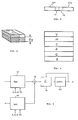
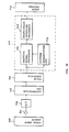
- a color copying machine or copier as an image information processing apparatus in accordance with a preferred embodiment of the present invention incorporates a color image reading device shown in Fig. 1.
- Scanning-type proximity sensor unit 10 optically reads an image of paper document 12 placed on glass document table 14.
- White reference plate 16 is provided on table 14.
- Sensor unit 10 has elongated light source 18, self-focusing rod-lens array 20, and image sensing device 22 which is constituted by a linear array of a plurality of chips of imaging devices, e.g., linear CCD image sensors.
- Light source 18 illuminates document 12.
- Light reflected by document 12 is focused on linear image sensors 22a, 22b,... through rod-lens array 20.
- Output signals of image sensors 22 are supplied to data selector 26 respectively through signal amplifiers 24.
- Data selector 26 is constituted by a switching circuit such as an analog switch circuit, and selects one of input image readout signals, which is then transferred to analog-to-digital converter (to be referred to as "A/D converter” hereinafter) 28.
- A/D converter analog-to-digital converter
- sensor unit 10 Before document 12 is read, sensor unit 10 reads black and white reference signals.
- the black reference signal is read such that image sensors 22 are operated while light source 18 is deactivated and light incident on sensor unit 10 is shielded.
- the white reference signal is read such that light emitted from light source 18 and reflected by white reference plate 16 is introduced to image sensors 22.
- an output signal of data selector 26 (i.e., an image readout signal of a selected one of two linear image sensors) is converted by A/D converter 28 into a digital signal, which is stored, through adder 30, in first line memory (“black reference line memory”) 32, the output of which is fed back to adder 30.
- the digital black reference signal contains random noise and drift noise components generated by image sensors 22 and amplifiers 24.
- the black reference signal is read several times, and the read results are averaged.
- the average signal is stored in line memory 32. In this case, if the number of times of average addition is a power of "2", an average value can be obtained by repeating shift processing. It should be noted that when specific processing is required in view of noise characteristics, the storage content of line memory 32 is read out, and resultant data may be restored in line memory 32 after the processing is completed.
- Sensor unit 10 is then moved to optically read paper document 12.
- the document image read by the linear array of image sensors 22 is amplified by amplifiers 24, and is converted to digital image data by A/D converter 28, thereby obtaining color document read signal X and white reference signal ⁇ W subjected to subtraction with the content of line memory 32.
- These signals X'and tW are supplied to multiplexer 42, as shown in Fig. 1.
- Multiplexer 42 combines these signals to produce multiplexed image signal 44.
- Multiplexed image signal 44 is input to non-linear converter 46 comprising a RAM (Random Access Memory).
- RAM 46 receives and stores data for color conversion suitable for an output printer supplied from a CPU (not shown). More specifically, if the output printer is a frame-sequential recording apparatus such as a color thermal printer or a color laser printer, suitable data is set to scan document 12 when a yellow signal is output. When magenta, cyan, and black (four color printing) signals are output, suitable data is set for every scanning, and scanning is repeated in units of colors. In this case, RAM 46 receives RGB signal 119, the non-linear content of which is switched in accordance with color separation signals R, G, and B of an input signal.
- RGB signal 119 the non-linear content of which is switched in accordance with color separation signals R, G, and B of an input signal.
- switching signal (Ch) 50 is also input to RAM 46.
- a logarithmic conversion is employed as a non-linear conversion.
- Non-linear converter 46 logarithmically converts signals X' and W', and multiplies the converted signals with a constant.
- read signal X' of document 12 is first subjected to non-linear conversion, and is stored in latch 48. Subsequently, white reference signal W' is subjected to non-linear conversion, and is transferred to adder 50.
- Adder 50 serves to subtract non-linear converted white reference signal W from the storage content (i.e., non-linear converted read signal X') of latch circuit 48.
- the output signal from adder 50 represents a document-readout image signal which is standardized (i.e., subjected to shading compensation) based on the white reference signal.
- the shading-compensated image signal is stored in one of three latch circuits 52, 54, and 56 in accordance with red, green, and blue color components.
- the output signals from latch circuits 52, 54, and 56 are supplied to adding circuit 58 to be added to each other.
- the output signal from adding circuit 58 is supplied to second non-linear converter 60 comprising a ROM, and is compensated thereby to match printing characteristics of a color printing machine or color printer unit (not shown) connected thereto.
- the output signal of second non-linear converter 60 serves as a signal for controlling color ink amounts of the printer.
- Black and white reference signals output from line sensors 22 are respectively given as B and W, a color document read signal is given as x, and respective color separation components are given by the following relations:
- Document read signal Y N from which black reference signal B is subtracted and is normalized by white reference signal IW i.e., subjected to shading compensation
- log X N log(X-B) - log (W-(B) (3)
- D is represented as follows: Equation (4) can be rewritten in units of color components as follows:
- component Dy is expressed as follows:
- input signal X is subjected to shading compensation in accordance with black and white reference signals B and W, and is then subjected to color compensation (masking processing) by matrix A.
- B is subtracted from signals X and I W, non-linear conversion aijlog is then performed, and subtraction and addition can then be performed.
- Non-linear processing for converting a color-compensated (masking-processed) signal to one suitable for a color printer will be explained below.
- a case will be described wherein a density on an ink surface is substantially constant like in a thermal color printer or a laser beam color printer, and is controlled by an ink dot area.
- Dy in equation (6) is represented as a relative density with respect to a solid yellow ink. If a reflectivity of the solid yellow ink is given as p, and a reflectivity at that time is given as R, Dy is expressed as follows: Thus, reflectivity R is expressed as: This value corresponds to reflection when ink having reflectivity p has thickness Dy in Fig. 2. In contrast to this, as shown in Fig.
- reflectivity R obtained when ink having reflectivity p is covered with dot area S is given by: If R in equation (9) is equal to R in equation (8), relative density Dy can be expressed by dot area S. More specifically, when the above relation is stored in ROM 60 serving as the second non-linear converter, data is converted to dot area S. The image signal can be output to the printer in accordance with this amount. Note that although p differs in accordance with spectral characteristics of a color separation filter, good results can be obtained if it is about 0.1. In addition, p is preferably changed in accordance with inks (Y, M, C) to perform appropriate conversion. In this case, ROM 60 requires a switching signal.
- a color compensation technique when a plurality of color line sensors are used will be described. This technique is based on the principle described in Japanese Patent Application Serial No. 60-240,974.
- two line sensors 22a and 22b are arranged adjacent to each other to read a one-line image. Assume that a color of right region 62 of line sensor 22 is slightly different from that of left region 64 of line sensor 22b.
- a color test chart of six colors (Y, M, C, R, G, B) shown in Fig. 4 is placed on document table 14, and is read.
- a signal of a j ink document obtained when it is read using a reference line sensor is given as Xoj
- a signal subjected to shading compensation of equation (3) is given as X LNoj .
- reference density signal Doi at that time is expressed as follows:
- J Matrix A 1 for minimizing error E can be obtained by: (where t indicates transposition. - 1 indicates an inverse matrix).
- a signal of sensor region 62 can be approximated to a reference signal.
- a signal of sensor region 64 can be similarly approximated to the signal of region 62 in the same manner as described above. More specifically, density signal Di j of region 62 is calculated based on A1 and X LN1j obtained by equation (13) in the same manner as in equation (11). Signal X LN2j of region 62 compensated by equation (3) is then calculated, and A 2 is calculated as follows in the same manner as in equation (13): Non-linear conversion data corresponding to matrices A 1 and A 2 (corresponding to equation (6)) are switched in accordance with read signals from line sensors 22a and 22b, thereby eliminating a difference between the two line sensors.
- Output signal Dk of a black ink output in the case of an output for a four-color printer can be obtained by the following equation in the same manner as in equation (5):
- FIG. 5 shows only a portion different from that in Fig. 1 showing the first embodiment, and other portions are the same as those in the first embodiment of Fig. 1.
- two non-linear conversion RAMs 70 and 72 are used to improve a processing speed. More specifically, read signal X' from which a black reference signal is subtracted, and white reference line memory output W ' are respectively input to RAMs 70 and 72, and are linearly converted in the same manner as in the above embodiment. The converted signals are subtracted from each other by adder 74, and the subtraction result is stored in latch circuit 78 through adding circuit 76.
- the signal is read out from latch circuit 78 in units of color separation signals in the same manner as in the first embodiment, and is subjected to the calculation of equation (5).
- adding circuit 76 and latch circuit 78 are simplified as compared to the above embodiment.
- RAMs 46, 70, and 72 can be replaced with ROMs, and ink color components of printers can be prestored therein. In this case, a switching signal must be input to the ROMs to output ink signals.
- non-linear conversion RAMs 46, 70, and 72 used in the above embodiments is limited to logarithmic conversion.
- ROMs 80 and 82 constituting a logarithmic conversion section are arranged to respectively receive document image read signal X' and white reference signal W'.
- the output signals from these ROMs are supplied to adder 84, and are subtracted from each other.
- the subtraction result is supplied to calculation circuit 86 which comprises a ROM to calculate equation (5).
- the output signal of RAM 86 is stored In latch 92 through sum calculator 90. According to this circuit arrangement, RAM 86 must have a larger capacity than the above embodiments in order to perform calculations with high precision.
- the characteristic feature of this embodiment is as follows: in an apparatus for reading a color image using a plurality of image sensors and color separation filters, a light source having a discontinuous light emission spectrum is used in place of a light source having a continuous light emission spectrum.
- a plurality of array elements CCD color sensors
- a coefficient of a matrix circuit is changed for each array element to perform compensation.
- a transmittance in two wavelength ranges excluding a main transmission wavelength is sufficiently low.
- a discontinuous 3-wavelength type light source since a discontinuous 3-wavelength type light source is used, an unstable portion with variations of the spectral distribution of a color separation filter is not used but a relatively stable portion is selectively used. Thus, if the entire spectral distribution of the color separation filters varies, relatively stable color signals can be obtained.
- the spectral distribution of the three wave lengths is appropriately determined to improve color separation characteristics.
- a coefficient of a matrix circuit is changed for each array element to perform compensation, so that color ununiformity can be compensated to a level that cannot be visually distinguished.
- a variation in spectral distribution of a color separation system can be equivalent to a sensitivity variation (brightness variation).
- a color read signal is divided by a signal obtained by reading a white reference plate (corresponding to shading compensation), thereby compensating for the variation, and eliminating color ununiformity.
- Fig. 7 shows a circuit arrangement for embodying the above principle of color compensation technique.
- Elongated light source 96 comprises a 3-wavelength type light source which has discontinuous spectral distribution characteristics.
- Light emitted from light source 96 and reflected by paper document 12 is guided to linear image sensor unit 108 through an optical path constituted by mirrors 98, 100, and 102, lens 104, and mirror 106, and is then focused thereonto.
- Image sensor unit 108 has four color CCD image sensor chips, as shown in Fig. 7.
- Each color linear image sensor has a color filter in which R, G, and B color filter elements are sequentially arranged, as shown in Fig. 8.
- image sensor unit 108 i.e., image read signals are supplied through amplifier 110 and A/D converter 112 to shading compensator 114, which standardizes (normalizes) a document image readout signal using a black reference signal and a white reference signal obtained by optically reading a white reference plate (see Fig. 1), thereby compensating for sensitivity ununiformity among sensors of sensor unit 108 and illumination ununiformity of light source 98, as disclosed in Japanese Patent Application No. 59-192663.
- a matrix compensating circuit disclosed in, e.g., Japanese Patent Application No. 60-240,974 is used to optimize a coefficient of a matrix for each sensor element.
- a solid curve represents spectral distribution characteristics (including spectral sensitivity of a sensor) of color separation filters Fr( ⁇ ), Fg( ⁇ ), and Fb(X) which are arranged on color light receiving sensor 108.
- a broken curve in Fig. 9 represents spectral distribution L( ⁇ ) of 3-wavelength type light source 96.
- sensor output Oij is expressed as follows: Since the reflection spectral characteristics of the white reference plate are substantially 1, output Oiw obtained by reading the white reference plate is expressed as: Therefore, if the light emission spectra of the 3-wavelength type light source are respectively given as linear spectra Xr, ⁇ g, and ⁇ b, and a light emission intensity thereof is set to be 1, signal Xri of an r sensor normalized by the white reference signal is given by: If Fr( ⁇ g)/Fr( ⁇ r) and Fr( ⁇ b)/Fr( ⁇ r) are sufficiently smaller than 1 and can be ignored, equation (18) can be rewritten as follows: As can be understood from equation (19), the sensor signal is not affected by color separation filters (including spectral sensitivity of the sensor).
- color separation filters when the spectral characteristics of color separation filters have sufficiently low transmittance in two wave length ranges (e.g., ⁇ g and Xb) excluding a main transmission wavelength (e.g., ⁇ r) in spectra of three wavelengths, color ununiformity can be removed. In this case, the color variation among color light receiving elements (e.g., color CCD sensors) and the color ununiformity in color light receiving elements can also be removed. For this reason, matrix circuit 116 shown in Fig. 7 may be omitted.
- the linear light emission spectra are assumed for the sake of simplicity. However, the present invention is not limited to the linear light emission spectra. In this case, a transmittance in other two wavelength ranges excluding the main transmission wavelength must be sufficiently decreased.
- the light emission intensity is not limited to 1, either.
- the color separation output signals are preferably substantially equal to each other.
- color separation signal Xrj is influenced by the color separation filter.
- Fig. 9 if light emission spectra are set in a relatively small variation portion of the spectral distribution, color ununiformity caused by the color separation filter can be eliminated. In this case, since the color ununiformity is large among the color light receiving elements (chips), a matrix circuit shown in Fig. 7 is necessary.
- the shading compensation for compensating for noise components caused by sensitivity variations of light receiving sensors, the illumination ununiformity, the matrix compensation for performing color compensation among a plurality of image sensors, and masking processing for performing color compensation for obtaining outputs to a color printer are achieved not by individual circuit elements but by non-linear conversion and addition/subtraction. Therefore, a complicated circuit such as multipliers need not be used, and a circuit arrangement can be greatly simplified. Since non-linear conversion can be achieved by almost one-dimensional conversion, precise calculation can be performed by a small-capacity memory, thus allowing fine color compensation and color reproduction with high fidelity.
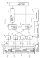
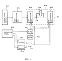
- An image reading device shown in Fig. 10 can be applied to the color copying machine of the present invention, wherein proximity color image sensing unit 200 has a plurality of chips of color linear CCD image sensors 202a, 202b, 202c, and 202d, which are zig-zag arrayed along main scanning direction X on mother plate 204.
- each image sensor chip 202 has an array of 1,024 photosensing elements or pixels, each of which has a size of 62.5 ⁇ m x 62.5 ⁇ m.
- Image sensing unit 200 can read an image on a B5-sized paper document at a resolution of 16 dots/mm.
- Image sensors 202 are associated with analog line memories 206a, 206b, 206c, and 206d, respectively. As shown in Fig. 10, adjacent sensor sub-units of image sensors 202 and analog line memories 206 have reversed arrangements, thereby preventing generation of nonphotosensitlve cell regions in the sensor sub-units along main scanning direction X.
- Analog line memories 206 are provided to compensate for a read delay time in sub-scanning direction Y.
- Each image sensor 202 of linear image sensing unit 200 receives a clock signal generated by clock generator 208 through CCD driver circuit 210.
- Linear image sensing unit 200 is connected to amplifier circuit 212.
- Amplifier circuit 212 includes amplifiers 212a, 212b, 212c, and 212d, which are respectively connected to the outputs of image sensors 202a, 202b, 202c, and 202d of unit 200.
- Amplifier circuit 212 is connected to analog data selectors 214 and 216 in such a manner that two amplifiers 212a and 212c are connected to selector 214, whereas the remaining amplifiers 212b and 212d are connected to selector 216.
- Image read signals are subjected to delay compensation by analog line memories 206, and are then supplied to data selectors 214 and 216.
- Data selectors 214 and 216 each select one of CCD output signals (document image read signals) input from image sensing unit 200, which is sequentially supplied to 8-bit A/D converters 218 and 220.
- A/D converters 218 and 220 perform analog-to-digital conversion in synchronism with the clock signal from clock generator 208.
- A/D converters 218 and 220 e.g., converter 218, is connected to image signal output circuit 224 through digital delay line memory 222.
- Delay line memory 222 can perform 2,048-byte data delay compensation under the control of controller 226, if required.
- Circuit 224 receives delay-compensated digital image signals, and arranges these input signals to generate one line of time-sequential image signals along main scanning direction X as a color video output signal.
- Controller 226 serves to control the overall image processing described above. In particular, when delay compensation is executed in line memory 222, controller 26 sets an appropriate number of lines in analog line memories 202 included in image sensing unit 200, and additionally provided digital delay line memory 222 in accordance with the required number of lines to be compensated.
- Figs. 11 and 12 show modifications of the circuit arrangement of Fig. 10, wherein the same reference numerals denote the same parts as in Fig. 10, and a detailed description thereof will be omitted.
- a modification circuit of Fig. 11 is different from the embodiment of Fig. 10 in that A/D converters 230, 232, 234, and 236 corresponding to the number of CCD image sensors 202 of linear image sensing unit 200 are provided between amplifier circuit 212 and data selectors 214 and 216. More specifically, a CCD output signal of each image sensor sub-unit 206 is supplied to the A/D converter associated therewith through the corresponding one of the amplifiers.
- the circuit arrangement shown in Fig. 12 is suitable for a system in which image read signals requiring delay compensation and ones requiring no delay compensation are not separately processed.
- two neighboring amplifiers 212a and 212b of amplifier circuit 212 are connected to A/D converter 240, whereas the remaining two neighboring amplifiers 212c and 212d are connected to A/D converter 242.
- A/D converters 240 and 242 are respectively connected to digital data selectors 244 and 246.
- Digital data selector 244 has a first output connected to a first input of digital data selector 250 through delay line memory 248, and a second output directly connected to a second input of selector 250.
- selector 246 has a first output connected to a first input of digital data selector 254 through delay line memory 252, and a second output directly connected to a second input of selector 254.
- the outputs of selectors 250 and 254 are connected to image signal output circuit 224.
- read delay components which are generated in sub-scanning direction Y among linear CCD image sensors 202a, 202b, 202c, and 202d zig-zag arrayed along main scanning direction X, can be effectively compensated at high speed by delay line memory 222 or delay line memories 248 and 252 separately provided from image sensing unit 200.
- a required memory capacity (which defines the number of lines to be compensated) of linear image sensing unit 200 is determined on the basis of a variable range of a sampling pitch in sub scanning direction Y, and a delay amount of zig-zag arrayed linear image sensors 202 in sub-scanning direction Y.
- delay line memory 222 or delay line memories 248 and 252 which are externally arranged to unit 200 can meet the remaining capacity. Therefore, a magnification changing range of an image expansion/reduction function of image sensing unit 200 can be widened.
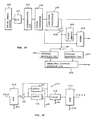
- a color phase compensating device shown in Fig. 13 can be applied to the color copying machine of the present invention: this color phase compensating device separates a compensation matrix into a unit matrix and a difference component matrix having a relatively small absolute value of each component, and performs a multiplication of the difference component matrix separately from the calculation of the unit matrix.
- a proximity sensor scanner unit which is generally designated by reference numeral "300"
- the CCD output signals of these image sensors of image sensing unit 306 are time-sequentially read out. These image sensor outputs are supplied through amplifiers 308 to analog multiplexer circuit 310.
- Analog multiplexer 310 multiplexes and combines the CCD output signals, each pixel signal of which includes R, G, and B color components, from the image sensors of image sensing unit 306, thereby producing one image read signal, which is then supplied to A/D converter 312 to be converted to a digital signal.
- shading compensator 3114 performs shading compensation so as to compensate for variations in brightness components included in the digital image signal, which inevitably occur due to brightness ununiformity of a document surface, sensitivity variations of color image sensors 306, and variations in color characteristics of color filters even if a document is scanned using uniform light source light.
- shading compensator 314 includes a line memory, which stores predetermined white and black reference signal data before a document is scanned. When a document image is read optically, the black reference signal is subtracted from a read image signal, and the subtraction result signal is divided by the corresponding white reference signal.
- a basic circuit arrangement therefor is disclosed in detail in Japanese Patent Application Serial No. 59-192,663.
- Shading compensator 314 compensates for illuminance ununiformity, a sensitivity variation of each light receiving element, and offset components. White balance compensation is performed at the same time. When a document is achromatic, compensated RGB signals are thus equal to each other. In particular, when a document image color is reference white or black, compensated RGB signals are 1 or 0.
- Shading compensator 314 can compensate for brightness components but cannot always compensate for a variation in color phase components.
- the variation in color phase components is mainly caused by a variation in color characteristics of the color filters, and hence, the variation occurs in units of sensor chips.
- the variation in color phase components is compensated by color phase compensator 316, which is connected to the output of compensator 314. More specifically, color phase compensation is performed such that RGB signals are multiplied with a compensation matrix corresponding to color characteristics of each sensor chip.
- RGB signals of each pixel are given by R, G, and B
- compensated RGB signals R', G', and B'
- Mn is a color phase compensation matrix for sensor chip n.
- color phase compensator 316 The operation principle of color phase compensator 316 according to the present invention will be described below.
- Color phase compensation can be performed by multiplying color image signals R, G, and B with compensation matrix Mn in the same manner as in the aforementioned embodiments.
- Color phase compensator 316 according to the present invention performs color phase compensation in accordance with equation (21).
- Fig. 14 shows the internal circuit arrangement of color phase compensator 316 of this embodiment.
- Calculator 320 may be constituted by adders and inverters.
- Color difference signals U and V output onto signal line 322 are supplied to matrix circuit 326 through register 324.
- Matrix circuit 326 calculates compensation difference RGB signal (AR, ⁇ G, ⁇ B) in accordance with the following equation:
- Chip selection signal 328 is a signal indicating a chip sensor by which color image signal 318 is being currently generated.
- RGB selection signal 330 is a signal which controls not to perform addition with corresponding RGB components when the compensation difference RGB signal (the output signal of this table) is subjected to addition in adder 334.
- the output signal of matrix circuit 326 is supplied to adder 334 as compensation difference RGB signal (AR, AG, AB) 332.
- Original RGB signal 318 is supplied to adder 334 through register 336.
- Adder 334 adds input signals 332 and 318 to obtain signal signal 338 representing compensated RGB signal (R', G', B').
- the signal transmission timing between registers 334 and 336 is synchronized so that a calculation is performed between signals of identical pixels.
- compensated RGB signal 338 is equivalent to the execution result of compensation calculation (equation (20), and color phase ununiformity among chips can be compensated.
- the absolute value of each component of matrix is sufficiently smaller than 1. For example, if each component is smaller than 1/16 (
- the circuit arrangement of color phase compensator 216 may be modified as shown in Fig. 15.
- R, G, B (1, 1, 1).
- optimal compensation matrix Mn does not always satisfy:
- the color phase compensator shown in Fig. 14 cannot realize such matrix compensation.
- color phase compensation which does not satisfy the white balance condition can also be realized.
- compensation difference RGB signal (AR, AG, AB) 342 is calculated by matrix circuit 340 in accordance with the following equation: where ⁇ " is a matrix obtained by subtracting unit matrix (I) from compensation matrix Mn as in the above embodiment of Fig. 14.
- this circuit is constituted by a look-up table.
- input RGB signal 318, chip selection signal 328, and selection signal 344 for designating one of AR, ⁇ G, and AB are used as an input address, and compensation difference signals ⁇ R, ⁇ G, and AB serve as output data.
- the size of this table is larger than that of the circuit of Fig. 14 since the number of input signals is increased.
- Compensation difference signals ⁇ R, ⁇ G, and AB output from the matrix circuit are added by adder 334 to original RGB signal 318, to obtain compensated RGB signal (R', G', B') 346.
- the signal transmission timing between registers 334 and 336 is synchronized so that a calculation is performed between signals of identical pixels in the same manner as in the embodiment of Fig. 14.
- Compensated RGB signal 346 thus corresponds to the execution result of the compensation calculation defined by equation (20) described above, and hence, color phase ununiformity among chips can be compensated effectively.
- an RGB filter such as a primary color filter is used as a color filter for each color sensor.
- the present invention may be also applied to other known color systems including a system employing CG and filters.
- the color difference signals may have any definition if color difference signals becomes 0 when an input signal represents an achromatic color, i.e., three color signals are equal to each other.
- a compensation matrix is separated into a unit matrix and a compensation difference matrix in which an absolute value of each component is small, and a color signal is multiplied with only the compensation difference matrix.
- a low-precision multiplier can be adopted, and circuit cost can be reduced.
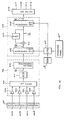
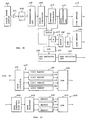
- scanning-type linear image sensing unit 400 has, e.g., four linear CCD image sensors 402a, 402b, 402c, and 402d, which are arrayed linearly or in a zig-zag manner along the main scanning direction of unit 400.
- CCD output signals (document image read signals) of these image sensors are supplied to pre-processing circuit 404.
- Pre-processor 404 includes amplifiers 406a, 406b, 406c, and 406d for respectively receiving and amplifying the CCD outputs.
- the output signals of the amplifiers are sequentially selected by switch circuit 408, and the selected signals are supplied to A/D converter 410 in a serial transfer manner.
- Digital color image signal Si obtained by A/D converter 410 includes R, G, and B components of a color separation filter (not shown in Fig. 16) used in each image sensor 402.
- Digital color image signal Si is supplied to shading compensating circuit 412, and is subjected to shading compensation processing (i.e., compensation processing of sensitivity ununiformity of image sensors 402, intensity ununiformity of document scanning light, and the like).
- the output signal of circuit 412 is normalized such that a signal level corresponding to a white region of a paper document (not shown in Fig. 16) is at logic "1" level, and a signal level corresponding to a black region of the paper document is at logic "0" level.
- the output signal of pre-processor 404 is generated in such a manner that R, G, and B signal components are generated in a time-sequential order, and these signals are supplied to color conversion circuit 414 of the present invention.
- Color conversion circuit 414 is a circuit for performing color conversion processing for optimizing hue and density of an input digital image signal to match with printing of a color hard copy using different color systems, such as yellow (Y), magenta (M), and cyan (C) inks, and further black (K) inks, if necessary, in a color printer (which comprises a known thermal transfer printer or laser printer) connected thereto.
- color conversion circuit 414 performs "two-step color adjustment processing" so as to prevent a problem in which the other parameter is changed and accurate adjustment of both the parameters cannot be performed.
- first color conversion circuit 416 is connected through adder 418 to second color conversion circuit 420.
- the output of adder 418 is fed back to the second input of adder 418 through latch circuit 422.
- Second color conversion circuit 420 produces frame-sequential ink amount signals Tj for designating amounts of Y, M, and C inks in printing a color hard copy by the printer (not shown).
- the output signal of second color conversion circuit 420 is supplied to switch circuit 424.
- First and second color conversion circuits 416 and 420 are connected to CPU 426.
- CPU 426 is connected to a table look-up memory such as RAM 428, and operation panel 430.
- Image signal Si input to color conversion circuit 414 is converted to intermediate color signal Dij as a third-system color signal.
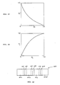
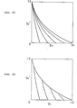
- Fig. 17 illustrates the relationship between parameters Si and Si" in equation (25).
- Function log (Si(1 - p) + p ⁇ /logp in equation (25) can be obtained such that storage data of table look-up memory 428 is read out in response to the operation of operation panel 430 by an operator under the control of CPU 426.
- Color conversion signals Dij output from first conversion circuit 416 include three color signal components DjR, DjG, and DjB, which are time-sequentially supplied to adder 418.
- Adder 418 sequentially adds signal components DjR, DjG, and DjB, and a sum signal is latched and stored in latch circuit 422, thereby obtaining color signal Dj.
- Color signal Dj is therefore represented by the following equation: According to equation (26), yellow signal DY can be obtained by "DYR + DYG + DYB", magenta signal DM can be obtained by "DMR + DMG + DMB”, and cyan signal DC can be obtained by "DCR + DCG + DCB". These color signals Dj (hue-compensated signals) are then supplied to second conversion circuit 420.
- Second conversion circuit 420 converts input signal Dj into ink amount designation signal Tj in accordance with an equation defined as follows:
- Fig. 18 shows the relationship between parameters Dj and Tj in equation (27).
- Function (1 - pDj)/(1 - p) in equation (27) can also be obtained such that storage data of table look-up memory 428 is read out in response to the operation of operation panel 430 by an operator under the control of CPU 426.
- ink amount designation signal Tj is output in such a manner that Y, M, C, and K ink components are time-sequentially generated.
- Ink color component signals are separated by switch circuit 424, and are supplied to a printer unit (not shown).
- the above-mentioned color conversion processing is based on the principle of a well-known "masking equation” described below.
- the following “masking equation” presented below is established between R, G, and B components of a read color (i.e., corresponding to signals Si), and Y, M, and C ink densities DY, DM, and DC for reproducing the colors upon printing: where M: 3 x 3 matrix coefficient
- M 3 x 3 matrix coefficient
- equation (28) requires high precision in a conversion circuit, and as a result, circuit cost is increased.
- equation (25) is used in place of the log function, and equation (27) is used so as to convert ink density signals DY, DM, and DC into ink amount designation signals Tj.
- intermediate color signal DKi for a black ink is calculated in accordance with input color signal Si: for ni >; 0
- Color signal DKi is supplied to adder 418, and its linear sum DK is calculated in the same manner as in DY, DM, and DC.
- Output color signal DK of adder 418 is converted to black-plate ink amount signal TK expressed by the following equation: for nK > ; 1 Ink amount signal TK obtained in this manner satisfies the above-mentioned conditions (a), (b), and (c), and assures reproduction of a good image with high contrast.
- functions of first and second conversion circuits 416 and 420 are switched or written upon only calculation of the black-plate signal.
- signal values of four colors, i.e., Y, M, C, and K can be calculated by an identical circuit.
- linear CCD image sensors 402a, 402b, 402c, and 402d in the embodiment described above have slightly different sensitivities and hue characteristics due to limitations on manufacture. (It is undesirable that if selection is performed to cause their sensitivities and color characteristics to strictly coincide with each other, manufacturing yield of products is decreased, resulting in an increase in cost of the apparatus.)
- "two-step color modulation" by first and second conversion circuits 416 and 420 of the present invention is important.
- first conversion circuit 416 contains four table look-up data tables therein. While a CCD output signal of first image sensor 402a is transferred to pre-processor 404, a first data table therefor is set in first conversion circuit 416 under the control of CPU 426. While a CCD output signal from second image sensor 402b is transferred to pre-processor 404, a second data table therefor is set in first conversion circuit 416.
- Matrix coefficient M is appropriately selected according to the following procedures so as to decrease or compensate for color ununiformity (difference in color tones) caused by a difference in color characteristics at boundary regions 430 and 432 of two adjacent ones of four CCD image sensors 402 in sensing unit 400, as shown in Fig. 19:
- a reference color k Y, M, C, R, G, B is read by image sensing unit 400 to obtain color signal Si.
- Average value Pkm of read signals Si of reference colors obtained at boundary pixel regions 430, 431, 432, 433, 434, and 435 (each of which has a size of 64 pixels or less) of two neighboring sensors 402a and 402b, 402b and 402c, and 402c and 402d of four image sensors 402 is calculated.
- P is a vector quantity consisting of three colors, i.e., R, G, and B.
- "k” is a suffix indicating Y, M, C, R, G, or B.
- "m” is a number for specifying a boundary pixel region at an end portion of each sensor.
- matrix coefficient M3 for a CCD output signal of third image sensor 402c is calculated so that color signal Si obtained in a pixel region located at substantially the center of image sensing unit 400, e.g., pixel region 433 at the left end region of third image sensor 402c, coincides with the reference color signal.
- color signal Dj corresponding to a reference color is given as target value Qk.
- Target value Qk can be calculated from ink dot area Qk' (which corresponds to ink amount designation signal Tj) in accordance with the following equation (31), which is an inverse conversion of equation (27):
- Matrix coefficient M3 can be calculated from value Qk and average value Pk4 from pixel region 433 (the suffix is 4, since pixel region 433 is a fourth end pixel region of image sensing unit 400 counted from the left) in accordance with the following equation: where "t": transpose
- a CCD output signal of second image sensor 402b i.e., matrix coefficient M2 for color signals, which optimizes average value Pk3 of produced color signals in pixel region 432 at the right end portion of second sensor 402b, is calculated using average value Pk4 of color signals from pixel region 433 and a value converted by matrix coefficient M3 for color signals from third image sensor 402c as a target value in accordance with the following equation:
- a CCD output signal of first image sensor 402a i.e., matrix coefficient M1 for color signals, which optimizes average value Pk1 of color signals produced in pixel region 430 at the right end portion of second sensor 402a, is calculated based on matrix coefficient M2 for color signals from second sensor 402b, color signals Pk2 from pixel region 431 at the left end portion of second sensor 402b, and color signals Pk1 from pixel region 431 at the right end region of first sensor 402a, in accordance with the following equation:
- matrix coefficient M4 for color signals from fourth sensor 402d is calculated in the same manner as described above in accordance with the following equation: where "Pk5" represents a color signal from pixel region 434 at the right end portion of third sensor 402c, and "Pk6" represents a color signal from pixel region 435 at the left end portion of fourth sensor 402d. It should be noted that the step of calculating matrix coefficient M4 may be performed between the step of calculating the average value and the step of determining matrix coefficient M3.
- Matrix coefficients M1 to M4 are stored in four table look-up table memory areas formed in first conversion circuit 416.
- Circuit 416 compensates for a difference or variation in color characteristics for each linear CCD image sensor 402 of image sensing unit 400, and performs color conversion processing free from color ununiformity.
- Fig. 20 shows the front view of operation panel 430, which comprises hue adjusting knob 440, saturation adjusting knob 442, density level selection switches 444, and background ununiformity reduction level selection switches 446.
- a hue rotational angle is set to be a given value by hue adjusting knob 440.
- This set value is transmitted to CPU 426.
- CPU 426 reads out basic data from ROM 428, and processes the basic data in accordance with the set hue rotational angle. Thereafter, CPU 426 writes the processed data in the table look-up memory of first conversion circuit 416.
- Fig. 21 shows a combination of 1/O characteristics in the conversion between Dj and Tj when five levels can be selected by density level selection switches 444, as shown in Fig. 21.
- the density conversion is performed by rewriting the table look-up memory in second conversion circuit 420, it does not affect a conversion operation of hue information in first conversion circuit 416 upon density conversion. Therefore, optimal I/O characteristics suitable for tone characteristics of an output apparatus such as a color printer can be obtained, and accurate color reproduction can be performed for any output apparatus.
- Figs. 22 and 23 show I/O characteristics in Si ⁇ - Si" conversion by equations (37) and (38) when five levels can be selected by background ununiformity reduction level selection switches 446, as shown in Fig. 21.
- the color adjustment for each color can be independently and easily performed.
- output signals Y, M, C, and K are output one by one in a frame-sequential manner.
- a means for storing color data may be additionally provided to adder 418, so that color signals Y, M, C, and K can be output simultaneously.
- Fig. 24 shows an embodiment wherein the contents of first and second conversion circuits 416 and 420 are switched to change output colors of a designated region.
- X- and Y-coordinate positions of a region for which output colors are to be changed are designated at operation panel 430, values indicating these coordinate positions are set in X- and Y-counters 450 and 452 before color signals are input.
- control signals ("1" level) are input from counters 450 and 452 to AND gate 454, and the contents of first and second conversion circuits 416 and 420 are respectively switched in response to the output signal from AND gate 454.
- the output colors are changed to those predetermined by the switched table look-up memory regardless of colors read by color image sensor 1.
- the output color signals are Y, M, C, and K but may be R, G, and B as in input color signals.
- the conversion equations in first and second conversion circuits 416 and 420 may adopt linear conversion. This embodiment is effective for an output apparatus such as a color CRT display which utilizes an additive mixture.
- a color image processing apparatus suitable for a color copying machine of the present invention, for changing spatial frequency characteristics and performing region detection processing based on image characteristics.
- the circuit arrangement is simplified as much as possible, and image regions such as color character patterns which have substantially the same luminance and have different hues can be effectively detected.
- color linear image sensing unit 500 is constituted by a combination of a plurality of the same linear CCD image sensors (not shown in Fig. 25) as in the above embodiments.
- Color image read signals from image sensing unit 500 are subjected to A/D conversion by A/D converter 502.
- the output signals of A/D converter 502, i.e., digital image signals, are supplied to compensation circuit 504.
- Circuit 504 normalizes the input image signals to compensate for variations in sensitivity and a difference in color characteristics among image sensors.
- the output signals from compensation circuit 504 are supplied to color converting circuit 506.
- Color converting circuit 506 has basically the same arrangement as that in the embodiment shown in Fig. 16 described above.
- circuit 506 converts input image color signals R, G, and B into ink amount designation signals Y, M, C, and K in a color printer unit such as a laser printer or thermal printer (not shown) in accordance with equations (39) presented below: In color converting circuit 506, calculations of ink amount signals Y, M, C, and K are independently performed.
- Color converting circuit 506 includes ROM 508 for sequentially receiving R, G, and B signals, as shown in Fig. 26.
- ROM 508 stores nine functions f YR , f vG , f YB , f MR , f MG , f MB , f cR , f cG , and fcB in the form of a table.
- One function is selected in response to switching control signal 510, and density function conversion is performed for an input color signal, e.g., an R signal.
- the output signal of ROM 508 is stored in latch circuit 514 through adder 512.
- the converted data is supplied to adder 512.
- Adder 512 calculates f YR (R) + f ⁇ c (G) + fy B (B).
- the calculation result is stored in latch circuit 518 in response to control signal 520. In this case, latch circuit 514 is reset.
- conversion function gy is selected in ROM 522, and ink amount designation signal Y is produced for a set of color signals R, G, and B in accordance with equation (39).
- Other ink amount signals M, C, and K are also produced in the same manner as described above.
- Ink amount designation signals Y, M, C, and K output from color converting circuit 506 are supplied to low-pass processor 528 of the present invention.
- Low-pass processor 528 performs 3 x 3 pixel averaging processing, and outputs signals (called “low-pass signals") from which high-frequency signal components are removed.
- Fig. 27 shows the internal circuit arrangement of low-pass processor 528 in detail.
- the three outputs of analog switch 530 are respectively connected to line memories 532, 534, and 536.
- Line memories 532 and 534 are connected through adder 538 to the first input of adder 540.
- Line memory 536 is connected to the second input of adder 540.
- the sum data from adder 540 is sequentially supplied to latches 542, 544, and 546.
- the storage data in latches 542 and 544 are added by adder 548, and the sum data is supplied to adder 550.
- Adder 550 adds the output data from adder 548 to the storage data in latch 546, thus obtaining the sum data of a given pixel and a 3 x 3 pixel region adjacent thereto.
- the output data from adder 550 is supplied to data converting circuit 552 including a ROM.
- the sum data of the 3 x 3 pixel region is divided by "9" by circuit 552, thus obtaining
- the output data of low-pass processor 528 is supplied to adder 554, which calculates a difference between the average data from circuit 528 and an original signal so as to obtain a so-called "Laplacian signal".
- the Laplacian signal is supplied to table memory 556 such as a ROM, and is multiplied with predetermined constant K. If original data is given as Y, and averaged data is given as Y, output signal X from adder 558 is defined by the following equation: Therefore, output signal X from adder 558 is a signal whose high-frequency components are emphasized.
- the output signal of adder 554, i.e., the Laplacian signal, is supplied to pattern matching circuit 560 for performing character region discrimination.
- Circuit 560 performs bi-level pattern matching of a 3 x 3 pixel region based on the input Laplacian signal when the ink amount designation signals after color conversion processing are obtained, thereby discriminating a character region.
- Fig. 28 shows an internal circuit arrangement of pattern matching circuit 560.
- the Laplacian signal from adder 554 is supplied to bi-level processor 562 including a ROM.
- Bi-level processor 562 binarizes the Laplacian signal at a predetermined level or more to produce a bi-level data signal.
- the bi-level data signal is stored in three 1-bit line memories 566,568, and 570 through multiplexer 564.
- the data signals stored in line memories 566, 568, and 570 are read out in units of thee pixels, and are input to character discrimination circuit 572 including a ROM.
- Circuit 572 produces a character discrimination signal when the input data signal in units of 3 pixels has a combination as a portion of a character pattern.
- processing of spatial frequency characteristics and region detection processing are performed for color signals of one or two colors which are obtained by color conversion from the read color image signals and include color components which are time-sequentially produced.
- a circuit for the processing of spatial frequency characteristics and region detection processing can correspond to every ink color (Y, M, C, and K) when parameters are changed upon each scanning, and can be commonly used for all the color signals. Therefore, a processing circuit need not be arranged for each color signal, and hence, the circuit arrangement can be simplified.
- region discrimination is performed based on a Laplacian signal of a color signal amount signal whose high-frequency components are emphasized by low-pass processor 528. In this manner, characters having an identical brightness (luminance) and different colors can be effectively discriminated.
- Fig. 29 shows a modification of the circuit shown in Fig. 25 (the same reference numerals in Fig. 29 denote the same parts as in Fig. 25).
- color conversion circuit 574 is different from that circuit 506 of Fig. 25 in that color signals R, G, and B and luminance signal I are calculated simultaneously.
- Luminance signal I is calculated by: The calculation data is stored in additional latch circuit 576 arranged in parallel with latch circuit 514 in color conversion circuit 574 shown in Fig. 30.
- the low-pass processed signal is converted to an ink amount signal whose high-frequency components are emphasized, by adder 554, constant multiplier 556 including a table memory, and adder 558 in the same manner as in the embodiment shown in Fig. 25.
- the Laplacian signal output from adder 554 is supplied to data selector 580.
- Data selector 580 separates signal components for designating an ink amount and signal components indicating a luminance from the Laplacian signal.
- the ink amount designation signal components are supplied to pattern matching circuit 560 in the same manner as in the embodiment shown in Fig. 25.
- Pattern matching circuit 560 performs character discrimination processing for the input color ink amount signal components.
- the luminance signal components of the Laplacian signal are supplied to another pattern matching circuit 582.
- Pattern matching circuit 582 performs character discrimination processing for the input luminance signal components.
- the output signals of these pattern matching circuits 560 and 582 are supplied to character pattern decision circuit 584, which performs total character region discrimination using a combination of the character region discrimination results of circuits 560 and 582, in other words, the character discrimination result for the color ink amount signal components and the character discrimination result for the luminance signal components. Therefore, discrimination precision can be improved.
- a color image processing apparatus shown in Fig. 31 suitable for a color copying machine of the present invention is featured in that "two-step picture segmentation processing" including rough and accurate picture segmentation operations is performed in order to allow a wide-range, high-precision picture segmentation of a read color image without requiring a large-capacity memory.
- output signals of scanning-type proximity image sensing unit 500 having linear CCD sensors are amplified by signal amplifier 602, and are then converted by A/D converter 604 to digital image signals.
- the output signals of A/D converter 604 are normalized by compensation circuit 606 which performs shading compensation processing.
- Color converter 608 receives the normalized color signals, and produces signals Y, M, C, and K for designating Y, M, C, and K ink amounts in the same manner as described above.
- Ink amount designation signals Y, M, C, and K are sequentially input to low-pass processor 610, and are subjected to 4 x 4 pixel averaging processing.
- the output signals of low-pass processor 610 are subjected to pixel thin-out processing by data compression circuit 612, thereby producing 1/16 pixel compressed signals. These signals are stored in multi-value line memory 614. Since 1/16 image compression processing is performed, the memory capacity of line memory 614 can be reduced to 1/16.
- Adder 616 calculates a difference between the output signal (original color image signal) from color converter 608 and the output signal (low-pass signals) from low-pass processor 610 to obtain a Laplacian signal representing a difference from the average value.
- This signal is supplied to adder 620 through ROM table memory 618 which multiplies an input with given constant K.
- Adder 620 adds this signal to the output signal (original color image signal) of color converter 608, and produces a color signal whose high-frequency components are emphasized.
- the output signal of adder 620 is binarized by bi-level ROM 622, and the bi-level signal is stored in bi-level image line memory 624.
- the output signal from adder 616 is supplied to a character discrimination unit which is constituted by bi-level ROM 626 and first and second decision circuits 628 and 630 so as to perform "two-step picture segmentation processing" of the present invention.
- the Laplacian signal output from adder 616 is binarized by bi-level ROM 626, and is supplied to first decision circuit 628 which performs local character decision.
- First decision circuit 628 performs primary character decision using a pattern matching technique based on a bi-level pattern of the Laplacian signal of a 4 x 4 pixel region consisting of a given pixel and pixels around it.
- first decision circuit 628 has data selector 632, the outputs of which are respectively connected to 1-bit line memories 634, 636, 638, and 640.
- the bi-level Laplacian pattern signals are sequentially selected by data selector 632 in units of 4 pixels, and are stored in the corresponding line memories.
- the storage contents of line memories 634, 636, 638, and 640 are supplied to pattern matching circuit 642 including a ROM.
- Circuit 642 produces a signal "1" when it detects a combination of data like a character in input data; otherwise, produces a signal "0".
- the output signal of first decision circuit 628 is then supplied to second decision circuit 630, which includes data compression circuit 644 (which is arranged to perform the same pixel thin-out processing as that in circuit 610 shown in Fig. 31), as shown in Fig. 33.
- the output signal of circuit 644 is sequentially selected in units of 4 x 4 pixels by data selector 646, and the selected signals are sequentially stored in 1-bit line memories 648, 650, and 652.
- the storage contents of line memories 648, 650, and 652 are supplied to pattern matching circuit 654 including a ROM in units of, e.g., 3 pixels.
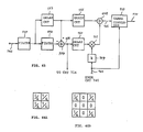
- ROM 654 stores pattern decision data shown in, e.g., Figs. 34A to 34F.
- ROM 654 discriminates that the input data (for pixel points indicated by marks " * " in Figs. 34A to 34C) is a character. If the input data coincides with any one of patterns shown in Figs. 34D to 34F, ROM 654 performs statistical processing as disclosed in, e.g., Japanese Patent Disclosure (Kokai) No. 60-204,177, thus performing rough character decision.
- Fig. 35 shows a modification of the circuit arrangement of Fig. 31, wherein the same reference numerals in Fig. 35 denote the same parts as in Fig. 31, and a detailed description thereof will be omitted.
- the circuit arrangement shown in Fig. 35 is featured in that a high-frequency emphasized signal is simultaneously subjected to binarization and Dither processing operations. More specifically, the output signal from adder 620 is supplied to dithering circuit 660 and binarization circuit 662.
- the dithered signal from circuit 660 is stored in 1-bit memory 664.
- the binarized signal from circuit 662 is stored in 1-bit memory 666.
- Data selector 668 selectively outputs binarized and dithered data in accordance with the decision result of second decision circuit 630.
- pattern matching circuit 630 discriminates three levels of pixel patterns: a signal for distinguishing a bi-level image of a character or line image from other images is produced onto first output signal line 670; a signal for designating whether a half-tone image pattern is subjected to multi-value or bi-level representation is produced onto second output signal line 672. For example, for the pixel pattern shown in Fig.
- a signal for specifying that dithered image data stored in memory 664 is employed is produced onto signal line 670, whereas a signal for specifying binarized image data is produced onto signal line 672.
- dithered image data is present between half-tone and bi-level image data, continuity of image data can be improved.
- a color image processing apparatus shown in Fig. 36 suitable for a color copying machine of the present invention, is featured in that optimal image processing (e.g., for a screen-tone image region, a high-frequency range is suppressed; for a bi-level image region, a filter gain is increased to perform high-frequency emphasis and the inclination of gamma characteristics is increased; and for a half-tone image, intermediate processing of the above two types of image regions is performed) is performed for discriminated various image components so as to allow outputting of a high-quality image (with low moire noise and high image resolution density) in which bi-level image, screen-tone image, and half-tone image (e.g., photograph image) components are mixed.
- a pattern matching process for image discrimination an input image is subjected to pattern matching to discriminate image types in units of pixel pattern regions having a size larger than a size 1/2 a dither matrix.
- color read image signals output from scanning-type proximity linear image sensing unit 700 are supplied to A/D converter 704 through amplifier 702.
- the digital image signals output from A/D converter 704 are supplied to color compensation circuit 706.
- the normalized image signals output from circuit 706 are supplied to color converter 708 which is arranged in the same manner as those in the above embodiments.
- Color converter 708 converts input image signals R, G, and B into ink amount designation signals Y, M, C, and K in the same manner as in the above embodiments.
- the ink amount designation signals are supplied to signal processing unit 710 of the present invention.
- Signal processing unit 710 modifies the input ink amount signals, and thus allows to produce a color hard copy so that a resolution and color tone of an input original image can be appropriately expressed in accordance with different types of image components included in the ink amount signals of an input image such as bi-level image components, screen-tone image components, and half-tone image components in image output unit 712 including a color printer such as a laser printer or thermal printer. More specifically, signal processing unit 710 performs signal processing for maximizing a resolution for bi-level image components included in the input image; and performs signal processing for improving tone characteristics and minimizing moire noise for screen-tone or half-tone image (photograph image) components included in the input image.
- Signal processing unit 710 has picture segmentation circuit 714, which performs, based on a character pattern matching technique, local picture segmentation processing for the ink amount signals of the input image, thereby extracting image regions corresponding to the bi-level image components, screen-tone image components, and half-tone image components included therein.
- a discrimination result signal (pattern matching result signal) generated from circuit 714 is supplied to adaptive signal processor 716.
- Circuit 716 serves to perform appropriate signal processing in accordance with the types of image components included in the input image.
- the optimized input image ink amount signals produced by circuit 716 are supplied to multi-level dithering processor 718.
- Picture segmentation circuit 714 has basically the same arrangement as that disclosed in Japanese Patent Disclosure (Kokai) No. 60-304,177. The operation of circuit 714 will be described below.
- Each ink amount signal input to circuit 714 is supplied to a low-pass processor (although not shown in Fig. 36) so that its low-frequency components are removed, thereby producing a Laplacian signal whose high-frequency components are emphasized.
- the Laplacian signal is binarized using an appropriate threshold value so as to obtain a Laplacian pattern having a two-dimensional pixel region pattern consisting of a given pixel of interest and pixels around it. Since the Laplacian pattern changes largely depending on the types of image, the pattern is checked to discriminate the type of input image with high probability.
- Figs. 37A and 37B exemplify such a Laplacian pattern.
- Figs. 37A and 37B "0"- and “1 "-level pixels of a bi-level signal are respectively indicated by marks " ⁇ " and "M”.
- Figs. 37C and 37D exemplify such a Laplacian pattern.
- the Laplacian pattern size resembles a distribution period of dots. If a wider pixel region is extracted, this tendency is enhanced.
- a half-tone image such as a photograph image
- a background portion of a character image a solid portion of a screen-tone image
- the Laplacian signal is substantially represented by "0" levels.
- Figs. 37E and 37F exemplify such a Laplacian pattern.
- a frequency of generation of a Laplacian pattern of each of the bi-level and screen-tone images in the input image changes as shown in Fig. 38.
- a Laplacian pattern is plotted along the abscissa of the graph in Fig. 38; a relative frequency is plotted along the ordinate.
- the Laplacian pattern has a pattern region generated for only a bi-level image (typically, region A), and a pattern region generated for only a screen-tone image (typically, region E).
- the types of an input image can be discriminated with high precision.
- the data shown in Fig. 38 is stored in a memory (not shown) included in picture segmentation circuit 714 shown in Fig. 36 in the form of a data table. The picture segmentation processing performed in circuit 714 can be effectively performed with reference this data table.
- Segmentation circuit 714 shown in Fig. 36 performs pattern matching in units of a pattern region of an input image having a size larger than a size at least 1/2 a dither matrix used in multi-value dithering processor 718, thereby detecting an image type.
- the pattern size of an input image to be subjected to pattern matching is set to be larger than a size 1/2 the dither matrix. This allows suppression or minimization of moire noise in an execution process of dither processing of an input screen-tone image.
- the Laplacian pattern of the screen-tone image is a repetitive pattern of pixels at a duty ratio of about 500/0, as shown in Fig. 39A.
- a high-density pixel region at least locally continues, as shown in Fig. 39B.
- Fig. 39D shows a case wherein a unit pattern size subjected to pattern matching is set to be 3/4 dither matrix p. If the pattern matching unit pattern size is increased to this size, pattern matching result data obtained in this region can have a sufficient content enough to determine whether the image pattern corresponds to either bi-level or screen-tone image. In other words, the pattern matching result data can have a sufficient content that can satisfactorily specify the feature patterns of various types of images. If the pattern matching unit pattern size is increased to be equal to a size 1/1 dither matrix p, as shown in Fig. 39E, the reliability of the pattern matching result can be further improved, and precision of picture segmentation can also be improved.
- segmentation circuit 714 of the present invention does not output a completely definite image type discrimination signal for specifying a single type of image based on the pattern matching result.
- segmentation circuit 714 of the present invention when a pattern matching result indicating that the input image pattern region is a bi-level image at a probability of 600/0 and is a screen-tone image at a probability of 400/0 is obtained (it may occur when the Laplacian pattern is included in region C of the graph shown in Fig. 38), segmentation circuit 714 of the present invention outputs a multi-value discrimination result signal in accordance with the probabilities of the image components. This multi-value discrimination result signal is called a "character-likelihood signal".
- a character-likelihood signal for each pattern is determined as follows. If relative frequencies for generation of pattern k in bi-level and screen-tone images are respectively given as Hc(k) and Hs(k), posterior probabilities Pc(k) and Ps(k) with which the pixels of pattern k correspond to a bi-level image and a screen-tone image (to be referred to simply as probabilities hereinafter) are respectively expressed as follows based on the Bayes theorem: where PcO, PsO, and P(k) are respectively probabilities of bi-level and screen-tone images in all the images, and a frequency of appearance of pattern k.
- Character-likelihood signal Q(k) of pattern is determined as follows as a logarithm of a ratio of Pc(k) to Ps(k) : (c: constant)
- a value near 0 is assigned as a character likelihood.
- Such assignment is effective since (1) relative frequencies of both a character image and a screen-tone image are high in the background portion, (2) intermediate processing between those for the character image and the screen-tone image is preferably performed as adaptive processing of the background portion, and so on.
- the character-likelihood signal obtained in this manner does not always have high discrimination precision, and randomly causes a discrimination error.
- causes therefor are (1) a Laplacian pattern is modified due to noise added to an input image signal, (2) patterns having high frequencies of appearance are present in both the bi-level image and the screen-tone image, and so on. For this reason, the discrimination precision of the character-likelihood signal is improved by the following large-area processor.
- a bi-level image region, a screen-tone image region, and a photograph image region are not mixed in a complicated manner.
- a given pixel is present in a bi-level image region, the possibility that the adjacent pixel is a bi-level image region is very high. Therefore, if a character-likelihood signal of the given pixel is very large, and all the character-likelihood signals of adjacent pixels are small, the character-likelihood signal of the pixel can be considered to be small.
- the large-area processor performs correction like this. As described above, the large-area processor also has an effect of smoothing a periodicity of the discrimination result of a screen-tone image.
- the large-area processor is realized by spatial smoothing of the character-likelihood signal. More specifically, if a characterlikelihood signal of pixel x is given as Q(x), Q'(x) is calculated as follows: (where y is a vector indicating a surrounding region)
- a signal obtained by appropriately quantizing Q'(x) is used as discrimination signal R as a final output of picture segmentation circuit 714.
- Q probability Pac that the region corresponds to a bi-level image and probability Pas that the region is a screen-tone image are respectively given by: Therefore, logarithm Qa of the ratio of these probabilities is as follows: That is, Q' represents a character likelihood in the smoothed region as in equation (44). If the type of pixel is discriminated in accordance with the level of character-likelihood signal Q', the discrimination result can be an optimal estimation under the above assumption, and high discrimination precision can be obtained.
- Fig. 40 shows a detailed internal arrangement of picture segmentation circuit 714 based on the above principle.
- Image signal 720 which is compensated/normalized by compensation circuit 706 for performing shading compensation shown in Fig. 36 is input to digital filter 722.
- Figs. 41 and 42 show the kernel and frequency response of digital filter 722.
- Filter 722 is one kind of Laplacian filter, and its output signal 724 serves as a Laplacian signal representing high-frequency components of an image.
- Laplacian signal 724 is binarized by binarization circuit 726 using threshold value T, which is set to be slightly larger than zero to provide a noise non-sensitive range for removing small noise components included in the input image.
- T threshold value
- the binarized signal output from binarization circuit 726 is supplied to pattern matching circuit 728.
- Pattern matching circuit 728 includes line memory section 730 and table memory 732.
- Table memory 732 stores reference decision data of Laplacian patterns.
- the binarized signal is transferred to line memory section 730, and is converted thereby to a two-dimensional Laplacian pattern.
- Pattern matching circuit 728 compares and collates the Laplacian pattern thus obtained with the storage pattern data in memory 732 to perform pattern matching processing, and specifies an image type (i.e., one of a screen-tone image, a bi-level image, and a half-tone image) of a pixel pattern region consisting of a pixel of interest and pixels around it. Circuit 728 then produces pattern matching result signal 734 for each pixel as the above-mentioned "character-likelihood signal".
- pattern matching result signal 734 is a 3-bit digital signal, which is obtained by quantizing a value calculated by equation (43) using seven threshold values at equal intervals (or can be at different intervals).
- the 3-bit digital signal is a multi-value signal which can have eight different signal levels. Use of a digital signal having such a number of bits contributes to save the capacity of pattern table memory 732.
- 3-bit digital signal 734 representing the pattern matching result is supplied to averaging circuit 736 including a smoothing circuit.
- Averaging circuit 736 performs averaging (smoothing) based on a convolutive addition for the 3-bit digital pattern matching result signal which is obtained for nine pixels consisting of a pixel of interest and eight adjacent pixels.
- the output signal from averaging circuit 736 is quantized by quantizer 740, thus producing 3-bit discrimination signal 742. Since discrimination signal 742 is a multi-value signal having eight levels of 0 to 7, a probability that an image component is a character for each level is defined as shown in Fig. 43. The probability data shown in Fig.
- discrimination signal 742 is level "2"
- a probability that the image is a character is 3 to 100/o
- discrimination signal 742 has level "7” it can be determined that the image is a character.
- multi-value discrimination signal 742 is supplied from segmentation circuit 714 to adaptive signal processor 716.
- Processor 716 performs optimal image processing corresponding to the decided type of image for ink amount signals Y, M, C, and K of an input original image in response to discrimination signal 742, thereby improving quality of an output image at thermal color printer 712 through multi-value dithering processor 718.
- Printer 712 produces a hard copy of a multi-tone color image based on an "area modulation method", and more preferably, a "multi-value dither method" as an extended version of an ordered dither method.
- Multi-value dithering processor 718 receives the adaptive-processed signal output from adaptive signal processor 716, and converts it into an n-value signal using (n-1) threshold values t1 to t(n-1), thereby producing a drive signal for a thermal printing head of printer 712.
- the drive signal is a signal for designating a pulse width to be supplied to heat-generation resistive elements (not shown) serving as recording elements of the thermal head of the printer.
- a heating amount of the thermal head is controlled to have n different levels for colors Y, M, C, and K, thus modulating recording ink amounts of a hard copy.
- the head drive signal is controlled to constitute one tone pattern using a set of a predetermined number of pixels corresponding to one dither threshold value matrix of a hard copy.
- the tone pattern is selected from six tone patterns a1 to a6 shown in Fig. 44 in accordance with a recording density of an image to be output. In this case, one tone pattern has 4 x 4 pixels. For example, in tone pattern a3, seven pixels arrayed in a cross shape are recorded upon application of appropriate current pulses, and the remaining nine pixels are not recorded at all.
- These tone patterns a1 to a6 have good tone characteristics in the corresponding density regions, and suppress noise caused by undesirable attachment of an ink to hard copy paper. Use of these tone patterns a1 to a6 allows printing of a high-quality hard copy. In particular, in generation of a hard copy of half-tone image components included in an input image whose image density changes moderately, natural print quality can be obtained.
- adaptive signal processor 716 compensates for a decrease in high-frequency components at the image sensor by high-frequency emphasis processing, and performs gamma conversion processing to make an edge portion of a character or line sharp, thereby preventing an unclear edge or a dotted edge caused by dithering.
- an original image is a screen-tone image
- a read image signal is passed through a low-pass filter for removing dither periodic components to prevent generation of moire noise caused by dither processing. Since gamma conversion processing impairs tone reproducibility, it is not performed when an original image is a tone image, i.e., a screen-tone image or a photograph image.
- the multi-value dither method can inherently assure certain image quality for both the bi-level and screen-tone images; moire noise is not caused for the screen-tone image unless a region which cannot be discriminated continues in a large area.
- pixels which cannot be discriminated are pixels having small features of the bi-level or screen-tone image. In this case, image degradation does not occur even if processing is performed using intermediate parameters.
- Image signal 746 supplied from shading compensation circuit 706 shown in Fig. 36 is input to first filter 748, and is subjected to 2 x 2 smoothing processing.
- the output signal from first filter 748 is supplied to second filter 750.
- Figs. 46A and 46B respectively show kernels of these filters 748 and 750.
- the output signal from first filter circuit 748 is also supplied to delay circuit 752.
- Delay circuit 752 performs delay processing, and produces a delay signal which is delayed by one pixel in both main scanning and sub-scanning directions.
- the delay signal and the output signal from second filter 750 are supplied to subtractor 754.
- Subtractor 754 calculates a difference between the input signals, and produces difference signal 756.
- Difference signal 756 represents high-frequency components of an original image signal. The calculation of the high-frequency components is common to that in digital filter (serving as Laplacian filter) 722 in Fig. 40, which has been described with reference to Figs. 41 and 42. Therefore, difference signal 756 is commonly used in picture segmentation circuit 714 shown in Fig. 36.
- the output signal of delay circuit 752 is delayed by a certain number of pixels by delay circuit 758. Difference signal 714 is delayed by a certain number of pixels by delay circuit 760. Signal delay processing in delay circuits 758 and 760 is to compensate for a delay time in signal transmission due to execution of pattern matching processing for discriminating types of image.
- the output signal of delay circuit 760 is a delay signal representing high-frequency components. This signal is supplied to multiplier 762. When multiplier 762 receives a signal obtained by multiplying discrimination signal 742 supplied from quantizer 740 with constant k by constant memory 764, it multiplies the k-times discrimination signal with the output signal from delay circuit 760. The output signal of multiplier 762 is supplied to adder 764.
- Adder 764 adds the output signals of delay circuit 758 and multiplier 762 to produce high-frequency modulated signal 766.
- Gamma converter 768 is provided to receive high-frequency modulated signal 766 and discrimination signal 742.
- Gamma converter 768 performs gamma conversion processing of high-frequency modulated signal 766 in accordance with the discrimination result represented by discrimination signal 742.
- the output signal of gamma converter 768 is supplied as high-frequency modulated signal to adaptive signal processor 716 shown in Fig. 36.
- Gamma converter 768 performs conversion of input signal x (i.e., output signal 766 from adder 764) represented by the following equation:
- Processing parameters such as k, a, and b are switched in accordance with the discrimination result of the image type represented by discrimination signal 742 shown in Fig. 40, which is output from picture segmentation circuit 714.
- parameters k and a are respectively set to be -1 and 1 to remove components causing moire noise due to dither processing, and an inclination of gamma conversion curve is set to be 1 to assure tone characteristics.
- optimal processing can be performed if the original image is any of a bi-level image such as a character image, a line image or the like, a screen-tone image, and a photograph image, and a high-quality image output can be obtained. Even if a discrimination error occurs or a portion which cannot be discriminated is present, degradation in image quality can be minimized.
- averaging of 3-bit digital pattern-matching result signal 734 output from pattern matching circuit 728 shown in Fig. 40 is not limited to smoothing of signal 734 by averaging circuit 736.
- a background portion is regarded to have an intermediate characteristic between bi-level and screen-tone images, and a value approximate to 0 is assigned to the character-likelihood signal.
- the character-likelihood signal tends to be a value approximate to 0 at a boundary of regions (in particular at an edge portion of a bi-level image). More specifically, the background portion tends to be recognized as an intermediate image between bi-level and screen-tone images.
- the background portion is not regarded to be an intermediate region between bi-level and screen-tone images, and is regarded to be another dimension.
- a value corresponding to levels of probabilities of bi-level and screen-tone images is not assigned to the background portion as the character-likelihood signal; an independent code as the background portion is assigned thereto as a discrimination result.
- the large-area processor performs averaging, while pixels discriminated as the background portion are ignored. More specifically, character-likelihood addition is made excluding pixels as a background portion of those around a pixel of interest; division is made with the number of pixels including the pixels as the background portion.
- Another discrimination processing method as an extended version of this method may be proposed which is based on the fact that a background portion frequently appears in a photograph image region and appears around bi-level and screen-tone images and which does not ignore the background portion.
- background portion patterns if a very large number of patterns (background portion patterns) are generated in a background portion, they are discriminated as a photograph image region or an intermediate region.
- bi-level patterns are present to a certain degree or more and background portion patterns are also present, these patterns are discriminated as a bi-level image by a simple smoothing method.
- screen-tone patterns are present to a certain degree or more and background portion patterns are also present, these patterns are discriminated as a screen-tone image.
- bi-level and screen-tone image patterns are present to about the same degree, substantially the same discrimination as in smoothing is performed.
- This processing can be realized by performing. Addition for each pattern assigned to 3 bits of character-likelihood signal 734 shown in Fig. 40, and by making decision by majority after the sum is non-linearly weighted.
- a discrimination signal obtained based on such large-area processing is used, binarization can be reliably performed at an edge portion of a bi-level image, and a sharp output image can be obtained.
- An image around a screen-tone image and a photograph image can be smoothed, and a natural image can be obtained.
- signal processing unit 710 shown in Fig. 36 When signal processing unit 710 shown in Fig. 36 is applied to a conventional monochrome copying machine, color converting circuit 708 shown in Fig. 36 is omitted. In this case, signal processing unit 710 directly receives the output signal from compensation circuit 706 for performing shading compensation, i.e., a sensitivity-compensated image signal, and performs the same operation as described above.
- shading compensation i.e., a sensitivity-compensated image signal
Landscapes
- Engineering & Computer Science (AREA)
- Multimedia (AREA)
- Signal Processing (AREA)
- Facsimile Image Signal Circuits (AREA)
- Color Image Communication Systems (AREA)
- Image Processing (AREA)
Applications Claiming Priority (14)
| Application Number | Priority Date | Filing Date | Title |
|---|---|---|---|
| JP62083814A JPS63250281A (ja) | 1987-04-07 | 1987-04-07 | カラ−画像読み取り装置 |
| JP83814/87 | 1987-04-07 | ||
| JP62-156532A JPH012467A (ja) | 1987-06-25 | 画像読取り装置 | |
| JP62156531A JPS642477A (en) | 1987-06-25 | 1987-06-25 | Hue correcting device |
| JP156532/87 | 1987-06-25 | ||
| JP156530/87 | 1987-06-25 | ||
| JP62156530A JP2618893B2 (ja) | 1987-06-25 | 1987-06-25 | カラー画像処理装置 |
| JP156531/87 | 1987-06-25 | ||
| JP157933/87 | 1987-06-26 | ||
| JP62157933A JP2618894B2 (ja) | 1987-06-26 | 1987-06-26 | 画像信号処理装置 |
| JP62213534A JPS6455245A (en) | 1987-08-27 | 1987-08-27 | Color conversion device |
| JP213534/87 | 1987-08-27 | ||
| JP50189/88 | 1988-03-03 | ||
| JP63050189A JPH01222964A (ja) | 1988-03-03 | 1988-03-03 | 画像処理装置 |
Publications (2)
| Publication Number | Publication Date |
|---|---|
| EP0286414A2 true EP0286414A2 (fr) | 1988-10-12 |
| EP0286414A3 EP0286414A3 (fr) | 1990-01-17 |
Family
ID=27564735
Family Applications (1)
| Application Number | Title | Priority Date | Filing Date |
|---|---|---|---|
| EP88303136A Withdrawn EP0286414A3 (fr) | 1987-04-07 | 1988-04-07 | Appareil de traitement d'images en couleurs |
Country Status (2)
| Country | Link |
|---|---|
| US (1) | US4926251A (fr) |
| EP (1) | EP0286414A3 (fr) |
Cited By (9)
| Publication number | Priority date | Publication date | Assignee | Title |
|---|---|---|---|---|
| DE3843999A1 (de) * | 1987-12-25 | 1989-08-03 | Fuji Xerox Co Ltd | Bildlesevorrichtung |
| EP0395032A3 (fr) * | 1989-04-28 | 1991-04-03 | Konica Corporation | Appareil de traitement d'images en couleurs |
| WO1991015078A1 (fr) * | 1990-03-19 | 1991-10-03 | Eastman Kodak Company | Procede et appareil pour ameliorer le rendu des couleurs des images sur papier realisees a partir de cameras electroniques |
| EP0449528A3 (en) * | 1990-03-26 | 1992-02-19 | Canon Kabushiki Kaisha | Image processing apparatus and the method thereof |
| EP0463844A3 (en) * | 1990-06-25 | 1992-10-14 | Canon Kabushiki Kaisha | Image processing apparatus |
| EP0488724A3 (en) * | 1990-11-30 | 1992-12-16 | Canon Kabushiki Kaisha | Ink jet recording apparatus and method |
| EP1515537A3 (fr) * | 2003-09-11 | 2006-07-26 | Dainippon Screen Mfg. Co., Ltd. | Processeur de traitement d'images avec association d'information, système d'impression, procédé permettant la sortie de données de présentation, et programme |
| EP1806913A4 (fr) * | 2004-10-29 | 2008-08-20 | Seiko I Infotech Inc | Méthode de lecture de document, lecteur de document, dispositif de formation d image et scanner d image |
| EP1835723A3 (fr) * | 2006-03-17 | 2008-10-15 | Ricoh Company, Ltd. | Lecteur d'image, processeur d'image et programme informatique |
Families Citing this family (57)
| Publication number | Priority date | Publication date | Assignee | Title |
|---|---|---|---|---|
| JPH0614685B2 (ja) * | 1984-03-29 | 1994-02-23 | 株式会社東芝 | 画像信号処理装置 |
| US4876610A (en) * | 1986-12-25 | 1989-10-24 | Canon Kabushiki Kaisha | Image processing apparatus with binarization-error dispersal |
| US5225915A (en) * | 1989-06-09 | 1993-07-06 | Xerox Corporation | Image processing with noise enhancing operators for moire reduction and/or random dot generation |
| US5223922A (en) * | 1989-06-26 | 1993-06-29 | Seiko Instruments Inc. | Color picture image reading device with color correction function |
| JP2505889B2 (ja) * | 1989-08-31 | 1996-06-12 | キヤノン株式会社 | 画像処理装置 |
| US5189523A (en) * | 1989-11-27 | 1993-02-23 | Canon Kabushiki Kaisha | Image processing apparatus |
| JPH03230683A (ja) * | 1990-02-05 | 1991-10-14 | Konica Corp | 複写機 |
| US5270808A (en) * | 1990-08-03 | 1993-12-14 | Canon Kabushiki Kaisha | Color image processing with adjustment of computed recording color to match original color |
| US5283668A (en) * | 1990-08-28 | 1994-02-01 | Canon Kabushiki Kaisha | Image reading apparatus with image sensor having selectively readable segments |
| JPH05336373A (ja) * | 1992-06-04 | 1993-12-17 | Toshiba Corp | 画像記録装置 |
| EP0587450B1 (fr) | 1992-09-11 | 2004-11-17 | Canon Kabushiki Kaisha | Méthode et appareil de traitement d'image |
| US5523849A (en) * | 1993-06-17 | 1996-06-04 | Eastman Kodak Company | Optimizing edge enhancement for electrographic color prints |
| JP3262414B2 (ja) * | 1993-07-19 | 2002-03-04 | キヤノン株式会社 | 画像処理装置及び画像処理方法 |
| US6081254A (en) * | 1993-08-12 | 2000-06-27 | Hitachi, Ltd. | Color correction system of imaging apparatus |
| JPH07221889A (ja) * | 1994-02-09 | 1995-08-18 | Mita Ind Co Ltd | 画像形成装置 |
| JPH0818785A (ja) * | 1994-04-28 | 1996-01-19 | Ricoh Co Ltd | 画像出力装置 |
| US5587728A (en) * | 1994-04-29 | 1996-12-24 | International Business Machines Corporation | Optical feedback printer |
| JP3542685B2 (ja) * | 1995-06-27 | 2004-07-14 | セイコーエプソン株式会社 | マルチトーンをもつバイナリ画像の圧縮及び復元のための装置及び方法 |
| US6646759B1 (en) * | 1996-05-15 | 2003-11-11 | Canon Kabushiki Kaisha | Printing apparatus and image output control apparatus for processing image data using a dither pattern |
| JP3696345B2 (ja) * | 1996-10-03 | 2005-09-14 | 富士写真フイルム株式会社 | 画像処理方法及び装置 |
| JP3706708B2 (ja) * | 1997-01-31 | 2005-10-19 | キヤノン株式会社 | 画像形成システム及び画像形成方法 |
| JPH10222663A (ja) * | 1997-01-31 | 1998-08-21 | Yamaha Motor Co Ltd | 画像認識システム及び装置 |
| US6108442A (en) * | 1997-06-27 | 2000-08-22 | Minnesota Mining And Manufacturing Company | Characterization of color imaging systems |
| JPH1125222A (ja) * | 1997-07-08 | 1999-01-29 | Sharp Corp | 文字切り出し方法及び文字切り出し装置 |
| JPH1155534A (ja) * | 1997-07-29 | 1999-02-26 | Fuji Photo Film Co Ltd | 色変換・濃度階調補正方法およびそのカラープリンター |
| US6381349B1 (en) * | 1997-11-12 | 2002-04-30 | The University Of Utah | Projector/backprojector with slice-to-slice blurring for efficient 3D scatter modeling |
| US6791711B1 (en) * | 1998-06-24 | 2004-09-14 | Canon Kabushiki Kaisha | Image processing method, image processing apparatus, and recording medium |
| US6567571B1 (en) * | 1998-06-24 | 2003-05-20 | Canon Kabushiki Kaisha | Image sensing device capable of outputting image signals by blocks and processing circuit which processes image signals by blocks |
| AUPP702498A0 (en) * | 1998-11-09 | 1998-12-03 | Silverbrook Research Pty Ltd | Image creation method and apparatus (ART77) |
| KR100291192B1 (ko) | 1999-06-28 | 2001-05-15 | 박종섭 | 파이프라인된 부분 선형 근사 방식을 이용한 감마 보정 장치 |
| JP3973340B2 (ja) * | 1999-10-05 | 2007-09-12 | Necエレクトロニクス株式会社 | 半導体装置、配線基板、及び、それらの製造方法 |
| US6646763B1 (en) * | 1999-11-12 | 2003-11-11 | Adobe Systems Incorporated | Spectral color matching to a device-independent color value |
| US6624911B1 (en) * | 1999-11-17 | 2003-09-23 | Lexmark International, Inc. | Method and apparatus for correcting unadjusted threshold arrays for halftoning by use of transfer function tables |
| US6987576B2 (en) * | 2000-03-06 | 2006-01-17 | Canon Kabushiki Kaisha | Image forming apparatus with gamma conversion means |
| US6816284B1 (en) * | 2000-04-07 | 2004-11-09 | Color Aix Perts Gmbh | Multispectral color reproduction system with nonlinear coding |
| JP2003032542A (ja) * | 2001-07-19 | 2003-01-31 | Mitsubishi Electric Corp | 撮像装置 |
| US6900908B1 (en) * | 2000-09-20 | 2005-05-31 | International Business Machines Corporation | Method, system, and program for halftoning data for rendering in a multitone output device |
| US7006253B2 (en) * | 2001-04-30 | 2006-02-28 | Kabushiki Kaisha Toshiba | Image processing apparatus |
| US6987587B2 (en) * | 2001-09-19 | 2006-01-17 | Kabushiki Kaisha Toshiba | Multiple recognition image processing apparatus |
| US7636636B2 (en) * | 2001-10-12 | 2009-12-22 | Abbott Laboratories | Imaging microarrays |
| JP2004157858A (ja) * | 2002-11-07 | 2004-06-03 | Baldwin Japan Ltd | 読取装置 |
| US20040101208A1 (en) * | 2002-11-27 | 2004-05-27 | Vidar Systems Corporation | Apparatus and methods for averaging image signals in a media processor |
| US7324244B2 (en) * | 2003-03-20 | 2008-01-29 | Kabushiki Kaisha Toshiba | Image forming apparatus and image forming method |
| US7365880B2 (en) * | 2003-04-04 | 2008-04-29 | Kabushiki Kaisha Toshiba | Image processing apparatus and image processing method |
| US20050264849A1 (en) * | 2004-05-28 | 2005-12-01 | Kabushiki Kaisha Toshiba | Printer |
| GB2415566B (en) * | 2004-06-24 | 2006-09-20 | Hewlett Packard Development Co | Image processing |
| JP4365735B2 (ja) * | 2004-06-25 | 2009-11-18 | 大日本スクリーン製造株式会社 | 印刷物測定装置 |
| JP4247993B2 (ja) * | 2004-11-05 | 2009-04-02 | シャープ株式会社 | 画像検査装置、画像検査方法、制御プログラムおよび可読記憶媒体 |
| US7869094B2 (en) * | 2005-01-07 | 2011-01-11 | Mitcham Global Investments Ltd. | Selective dithering |
| US7515307B2 (en) * | 2005-07-26 | 2009-04-07 | Konica Minolta Systems Laboratory, Inc. | Enhanced image printing system |
| US7599556B2 (en) * | 2005-08-25 | 2009-10-06 | Joseph Stanley Czyszczewski | Apparatus, system, and method for scanning segmentation |
| US7586521B2 (en) * | 2006-01-27 | 2009-09-08 | Nethra Imaging Inc. | Automatic color calibration of an image sensor |
| US7616343B2 (en) * | 2006-04-06 | 2009-11-10 | Kabushiki Kaisha Toshiba | Image data conversion apparatus, image forming apparatus, image data conversion method and program |
| JP5147641B2 (ja) * | 2008-10-24 | 2013-02-20 | キヤノン株式会社 | 原稿読取装置 |
| JP6472336B2 (ja) * | 2014-06-18 | 2019-02-20 | キヤノン株式会社 | 画像処理装置、画像処理方法およびプログラム |
| JP6823962B2 (ja) * | 2016-07-27 | 2021-02-03 | 株式会社Screenホールディングス | インク消費量見積もり方法、インク消費量見積もり装置、および印刷システム |
| JP7543719B2 (ja) * | 2020-06-23 | 2024-09-03 | 株式会社リコー | シェーディング補正装置、読取装置、画像形成装置、及び方法 |
Family Cites Families (22)
| Publication number | Priority date | Publication date | Assignee | Title |
|---|---|---|---|---|
| US4194221A (en) * | 1978-12-26 | 1980-03-18 | Xerox Corporation | Automatic multimode continuous halftone line copy reproduction |
| JPS58105007A (ja) * | 1981-12-17 | 1983-06-22 | Toshiba Corp | 画像面積測定装置 |
| JPH0683371B2 (ja) * | 1982-10-20 | 1994-10-19 | キヤノン株式会社 | 情報読取り装置 |
| US4514738A (en) * | 1982-11-22 | 1985-04-30 | Tokyo Shibaura Denki Kabushiki Kaisha | Thermal recording system |
| EP0110353B2 (fr) * | 1982-11-30 | 1990-03-21 | Kabushiki Kaisha Toshiba | Système de traitement de signal d'image approprié à affichage d'images en demi-teinte |
| JPH0685186B2 (ja) * | 1983-01-25 | 1994-10-26 | 利之 坂井 | 写真領域識別装置 |
| JPS59156070A (ja) * | 1983-02-25 | 1984-09-05 | Canon Inc | 画像処理装置 |
| US4631578A (en) * | 1983-03-04 | 1986-12-23 | Canon Kabushiki Kaisha | Method of and apparatus for forming a color picture using a plurality of color correction processings |
| JPS6051816A (ja) * | 1983-08-31 | 1985-03-23 | Toshiba Corp | 読取装置 |
| JPS6091762A (ja) * | 1983-10-26 | 1985-05-23 | Canon Inc | 画像処理装置 |
| JPS60204170A (ja) * | 1984-03-29 | 1985-10-15 | Toshiba Corp | 画像読取り装置 |
| JPH0614685B2 (ja) * | 1984-03-29 | 1994-02-23 | 株式会社東芝 | 画像信号処理装置 |
| US4723173A (en) * | 1984-05-31 | 1988-02-02 | Canon Kabushiki Kaisha | Image processing apparatus |
| US4661843A (en) * | 1984-07-16 | 1987-04-28 | Kabushiki Kaisha Toshiba | Color image copying apparatus |
| JPS6180969A (ja) * | 1984-09-28 | 1986-04-24 | Fuji Xerox Co Ltd | 画信号処理装置 |
| US4821334A (en) * | 1984-12-28 | 1989-04-11 | Canon Kabushiki Kaisha | Image processing apparatus |
| US4724446A (en) * | 1985-01-31 | 1988-02-09 | Kabushiki Kaisha Toshiba | Thermal transfer printing apparatus |
| JPH0618414B2 (ja) * | 1985-03-30 | 1994-03-09 | 株式会社東芝 | カラ−画像読み取り装置 |
| JPS61285867A (ja) * | 1985-06-12 | 1986-12-16 | Dainippon Screen Mfg Co Ltd | 網点画像記録方法並びに装置 |
| US4745467A (en) * | 1985-10-28 | 1988-05-17 | Kabushiki Kaisha Toshiba | Color image-processing apparatus |
| JPS62111570A (ja) * | 1985-11-09 | 1987-05-22 | Fuji Photo Film Co Ltd | 画像入出力システムにおける出力信号処理条件の自動設定方法 |
| US4782398A (en) * | 1986-02-14 | 1988-11-01 | Canon Kabushiki Kaisha | Image processing apparatus |
-
1988
- 1988-04-06 US US07/178,431 patent/US4926251A/en not_active Expired - Fee Related
- 1988-04-07 EP EP88303136A patent/EP0286414A3/fr not_active Withdrawn
Cited By (15)
| Publication number | Priority date | Publication date | Assignee | Title |
|---|---|---|---|---|
| DE3843999A1 (de) * | 1987-12-25 | 1989-08-03 | Fuji Xerox Co Ltd | Bildlesevorrichtung |
| EP0395032A3 (fr) * | 1989-04-28 | 1991-04-03 | Konica Corporation | Appareil de traitement d'images en couleurs |
| WO1991015078A1 (fr) * | 1990-03-19 | 1991-10-03 | Eastman Kodak Company | Procede et appareil pour ameliorer le rendu des couleurs des images sur papier realisees a partir de cameras electroniques |
| US5245444A (en) * | 1990-03-26 | 1993-09-14 | Canon Kabushiki Kaisha | Image reproduction using error diffusion or dither matrix |
| EP0449528A3 (en) * | 1990-03-26 | 1992-02-19 | Canon Kabushiki Kaisha | Image processing apparatus and the method thereof |
| EP0463844A3 (en) * | 1990-06-25 | 1992-10-14 | Canon Kabushiki Kaisha | Image processing apparatus |
| EP0488724A3 (en) * | 1990-11-30 | 1992-12-16 | Canon Kabushiki Kaisha | Ink jet recording apparatus and method |
| EP0706889A1 (fr) * | 1990-11-30 | 1996-04-17 | Canon Kabushiki Kaisha | Appareil d'enregistrement à jet d'encre et méthode |
| US5745145A (en) * | 1990-11-30 | 1998-04-28 | Canon Kabushiki Kaisha | Ink jet recording apparatus and method |
| EP1515537A3 (fr) * | 2003-09-11 | 2006-07-26 | Dainippon Screen Mfg. Co., Ltd. | Processeur de traitement d'images avec association d'information, système d'impression, procédé permettant la sortie de données de présentation, et programme |
| US7903282B2 (en) | 2003-09-11 | 2011-03-08 | Dainippon Screen Mfg. Co., Ltd. | Image processing information association processor, printing system, method of enabling layout data output, and program |
| EP1806913A4 (fr) * | 2004-10-29 | 2008-08-20 | Seiko I Infotech Inc | Méthode de lecture de document, lecteur de document, dispositif de formation d image et scanner d image |
| US8054510B2 (en) | 2004-10-29 | 2011-11-08 | Seiko I Infotech Inc. | Document reading method, document reader, image forming device, and image scanner |
| EP1835723A3 (fr) * | 2006-03-17 | 2008-10-15 | Ricoh Company, Ltd. | Lecteur d'image, processeur d'image et programme informatique |
| US8159726B2 (en) | 2006-03-17 | 2012-04-17 | Ricoh Company, Limited | Image reader, image processor, and computer program product |
Also Published As
| Publication number | Publication date |
|---|---|
| US4926251A (en) | 1990-05-15 |
| EP0286414A3 (fr) | 1990-01-17 |
Similar Documents
| Publication | Publication Date | Title |
|---|---|---|
| US4926251A (en) | Color image processing apparatus with image corrector | |
| US5341226A (en) | Automatic image segmentation for color documents | |
| US6449060B1 (en) | Image processing apparatus and method | |
| US4876610A (en) | Image processing apparatus with binarization-error dispersal | |
| US6118547A (en) | Image processing method and apparatus | |
| US5565994A (en) | Multiple separation error diffusion, with cross separation correlation control for color images | |
| US5734801A (en) | Method of and apparatus for producing color proof | |
| US5325448A (en) | Image treatment method and apparatus with error dispersion and controllable quantization | |
| EP0702482B1 (fr) | Obtention de demi-teintes par diffusion d'erreurs avec réponse homogène dans des régions d'images de forte/faible intensité | |
| JP4213230B2 (ja) | カラードキュメントプリント方法 | |
| US5325211A (en) | Error diffusion with output and input based feedback | |
| US5321525A (en) | Clustered halftoning with dot-to-dot error diffusion | |
| KR100405226B1 (ko) | 다중레벨복수컬러입력이미지재생방법 | |
| US6192152B1 (en) | Image processing apparatus | |
| US8259357B2 (en) | Image processing apparatus, image forming apparatus, image processing method, and computer readable recording medium | |
| US4745467A (en) | Color image-processing apparatus | |
| GB2273017A (en) | Colour error diffusion dependent on neighbouring pixel gradation | |
| JPH05336373A (ja) | 画像記録装置 | |
| EP1366618B1 (fr) | Procede et systeme de diffusion d'erreur par points partiels | |
| US5157741A (en) | Image processing method and apparatus for out-putting dot-processed data with suppression of false contours and other noise | |
| EP0542513B1 (fr) | Appareil de lecture d'images en couleurs | |
| US6744921B1 (en) | Image processing apparatus and method that determines the thickness of characters and lines | |
| US5253083A (en) | Image reading apparatus having improved shading correction | |
| JPS62149258A (ja) | 画像処理方式 | |
| US6134355A (en) | Binarization using a local average, and using error diffusion |
Legal Events
| Date | Code | Title | Description |
|---|---|---|---|
| PUAI | Public reference made under article 153(3) epc to a published international application that has entered the european phase |
Free format text: ORIGINAL CODE: 0009012 |
|
| 17P | Request for examination filed |
Effective date: 19880420 |
|
| AK | Designated contracting states |
Kind code of ref document: A2 Designated state(s): DE FR GB IT |
|
| PUAL | Search report despatched |
Free format text: ORIGINAL CODE: 0009013 |
|
| AK | Designated contracting states |
Kind code of ref document: A3 Designated state(s): DE FR GB IT |
|
| 17Q | First examination report despatched |
Effective date: 19920214 |
|
| STAA | Information on the status of an ep patent application or granted ep patent |
Free format text: STATUS: THE APPLICATION IS DEEMED TO BE WITHDRAWN |
|
| 18D | Application deemed to be withdrawn |
Effective date: 19920625 |