EP0287031A2 - Hohe Durchbruchspannung aufweisende isolierende Schicht, die zwischen Polysilizium-Schichten liegt - Google Patents
Hohe Durchbruchspannung aufweisende isolierende Schicht, die zwischen Polysilizium-Schichten liegt Download PDFInfo
- Publication number
- EP0287031A2 EP0287031A2 EP88105805A EP88105805A EP0287031A2 EP 0287031 A2 EP0287031 A2 EP 0287031A2 EP 88105805 A EP88105805 A EP 88105805A EP 88105805 A EP88105805 A EP 88105805A EP 0287031 A2 EP0287031 A2 EP 0287031A2
- Authority
- EP
- European Patent Office
- Prior art keywords
- poly
- film
- layer
- impurity
- insulating film
- Prior art date
- Legal status (The legal status is an assumption and is not a legal conclusion. Google has not performed a legal analysis and makes no representation as to the accuracy of the status listed.)
- Granted
Links
Images


Classifications
-
- H—ELECTRICITY
- H10—SEMICONDUCTOR DEVICES; ELECTRIC SOLID-STATE DEVICES NOT OTHERWISE PROVIDED FOR
- H10D—INORGANIC ELECTRIC SEMICONDUCTOR DEVICES
- H10D64/00—Electrodes of devices having potential barriers
- H10D64/60—Electrodes characterised by their materials
-
- H—ELECTRICITY
- H10—SEMICONDUCTOR DEVICES; ELECTRIC SOLID-STATE DEVICES NOT OTHERWISE PROVIDED FOR
- H10D—INORGANIC ELECTRIC SEMICONDUCTOR DEVICES
- H10D64/00—Electrodes of devices having potential barriers
- H10D64/01—Manufacture or treatment
- H10D64/031—Manufacture or treatment of data-storage electrodes
- H10D64/035—Manufacture or treatment of data-storage electrodes comprising conductor-insulator-conductor-insulator-semiconductor structures
-
- H—ELECTRICITY
- H10—SEMICONDUCTOR DEVICES; ELECTRIC SOLID-STATE DEVICES NOT OTHERWISE PROVIDED FOR
- H10D—INORGANIC ELECTRIC SEMICONDUCTOR DEVICES
- H10D64/00—Electrodes of devices having potential barriers
- H10D64/60—Electrodes characterised by their materials
- H10D64/66—Electrodes having a conductor capacitively coupled to a semiconductor by an insulator, e.g. MIS electrodes
- H10D64/661—Electrodes having a conductor capacitively coupled to a semiconductor by an insulator, e.g. MIS electrodes the conductor comprising a layer of silicon contacting the insulator, e.g. polysilicon having vertical doping variation
- H10D64/662—Electrodes having a conductor capacitively coupled to a semiconductor by an insulator, e.g. MIS electrodes the conductor comprising a layer of silicon contacting the insulator, e.g. polysilicon having vertical doping variation the conductor further comprising additional layers, e.g. multiple silicon layers having different crystal structures
Definitions
- the present invention relates to a semiconductor device capable of improving a breakdown voltage on a thin insulating film formed between poly-Si layers, and to a method for manufacturing the same.
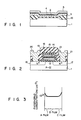
- FIG. 1 is a cross-sectional view showing one of manufacturing steps of a conventional EPROM.
- first thermal oxide film 2 of 500 ⁇ in thickness and field oxide film are formed over the surface of P ⁇ type silicon substrate 1, the field oxide film surrounding an element area.
- First poly-Si layer 3 of 1000 ⁇ in thickness, which is used as a floating gate electrode formation layer, is formed by means of a low-pressure chemical vapor deposition (CVD) method on field oxide film 1 and on first thermal oxide film 2.
- CVD low-pressure chemical vapor deposition
- Phosphorus are doped by means of a thermal diffusion method into first poly-Si silicon film 3.
- the surface of first poly-Si film 3 is thermally oxidized at about 1000°C, thereby forming second thermal oxide film 4 having a thickness of 500 ⁇ .
- Second poly-Si film 5 for control gate electrode formation is formed on the surface of a resultant structure by means of a low-pressure CVD method. Phosphorus are doped by means of a thermal diffusion method into second poly-Si film 5.
- Fig. 2 is a cross-sectional view showing a model of a conventional EPROM. An explanation will be given below of the process for manufacturing a conventional EPROM, by referring to Figs. 1 and 2 (a complete view).
- Second poly-Si film 5, second thermal oxide film 4, first poly-Si film 3 and first thermal oxidation film 2 are sequentially etched by means of a photoetching method.
- control gate electrode 15, second gate oxide film 14, floating gate electrode 13 and first gate oxide film 12 are formed in the semiconductor structure as shown in Fig. 2.
- N-type impurity is ion-implanted into a surface portions of the semiconductor structure 1 using control gate electrode 15, second gate oxide film 14, floating gate electrode 13 and first gate oxide film 12 as masks.
- Substrate 1 is heat-treated, thereby diffusing the N-type impurity deep into substrate 1.
- N+ type drain region 16 and N+ type source region 17 are formed in the semiconductor substrate.
- the surface of the resultant structure is thermally oxidized to provide thermal oxide film 18 with which the surfaces of substrate 1 and control gate electrode 15, as well as the side surfaces of second gate oxide film 14, floating gate electrode 14 and first oxide film, are surrounded.
- Passivation layer 19 such as a PSG film, is deposited on the whole surface of the resultant surface.
- Passivation layer 19 is selectively etched to form contact holes. As a result, the portions of drain region 16 and source region 17 are exposed at the locations of the contact holes.
- An Al-Si layer is deposited wholly on the surface of the resultant structure, followed by a patterning step to provide drain electrode 20 and source electrode 21. In this way, a conventional EPROM is completed as shown in Fig. 2.
- the EPROM is of such a type that it allows the writing of data by the application of a high positive voltage across N+ type drain region 16 and control gate electrode 15 and the injection of electrons into floating gate electrode 13.
- second poly-Si film 5 for the formation of control gate electrode 15 After the deposition of second poly-Si film 5 for the formation of control gate electrode 15, phosphorus are doped by a thermal diffusion method into second poly-Si film 5.
- thermal treatments are performed at the steps including the formation of thermal oxide film 18.
- Phosphorus are doped into first poly-Si film 3 and second poly-Si film 5 and migrated toward first thermal oxide film 2 and second thermal oxide film 4, respectively.
- first poly-Si film 3 and second poly-Si film 5 are as shown in Fig. 3. That is, the phosphorus concentration becomes higher at the outer edge portions A and C of first poly-Si film 3 and second poly-Si film 5.
- first thermal oxide film 2 and second thermal oxide film 4 This means that the phosphorus are diffused into first thermal oxide film 2 and second thermal oxide film 4. As a result, the close density of first thermal oxide film 2 and second thermal oxide film 4 is reduced to reveal the electrical conductivity. The breakdown voltage is thus reduced, permitting the ready electron migration.
- control gate electrode 15 When a high voltage is applied to control gate electrode 15, electrons stored in floating gate electrode 13 is absorbed in control gate electrode 15 via second gate oxide film 14.
- the object of the present invention is to provide a semiconductor device capable of improving a breakdown voltage on a thin insulating film provided between poly-Si layers and a method for manufacturing the same.
- a semiconductor device which comprises a first insulating film formed on a major surface of a semiconductor substrate, a film of silicon other than a single crystal silicon formed on the first insulating film and having either a phosphorus concentration which is lower than the concentration in the first film or contains no phosphorus, a first poly-Si film formed on the film of silicon and having a higher phosphorus concentration than that of the film of silicon, a second poly-Si film formed on the first poly-Si film and having a lower phosphorus concentration than that of the first poly-Si film or containing no phosphorus, and a second poly-Si film formed on the second poly-Si insulating film.
- the non-single crystal silicon film adjacent to the first insulating film and second poly-Si film adjacent to the second insulating film have a lower phosphorus concentration, phosphorus in the non-single silicon film and second poly-Si film are not diffused into the first insulating film and the breakdown voltage of the first and second insulating films is improved.
- a method for manufacturing a semiconductor device which comprises the steps of forming a first insulating film on a major surface of a semiconductor substrate; forming, on the first insulating film, a non-single crystal film having a lower phosphorus concentration or never containing any phosphorus; forming a first poly-Si film on the non-single crystal film at a temperature higher than when the non-single crystal silicon film is formed, the first poly-Si film having a higher phosphorus concentration than that of the non-single crystal silicon film; forming on the first poly-Si film a second poly-Si film having a lower phosphorus concentration or never containing any phosphorus; and forming a second insulating film on the second poly-Si layer.
- first and second poly-Si films are formed over an underlaying non-single crystal silicon film having an assumed high concentration profile of silicon atoms as adsorption spots in which case the first and second poly-Si films have a particle size of, for example, below 100 ⁇ so that the first and second poly-Si films become denser. Since the phosphorus impurity is doped upon forming the first and second poly-Si films, the manufacturing process can be shortened unlike the case where, in the conventional method, phosphorus are diffused into the poly-Si film after the poly-Si film has been formed.
- the second insulating film Even if the second insulating film is formed over the resultant structure, since the second poly-Si film contains small grains, the enhancement of an electric field at an interface resulting from the unevenness of the crystal is reduced to a greater extent. Further technically, since the second poly-Si film of a lower phosphorus concentration is formed over the first poly-Si film, even if the second insulating film is formed on the second poly-Si film, the diffusion of the phosphorus into the second insulating film is decreased, thus improving the breakdown voltage of the second insulating film.
- First thermal oxide film (insulating film) 52 of 500 ⁇ in thickness is formed by a thermal oxidation method on the surface of substrate 51 at 700°C to 1100°C in either a dry O2, H2O, or HCl + O2 atmosphere (Fig. 4A).
- Silicon film 53 of at least 30 ⁇ being other than a single crystal type is deposited by a LPCVD method on the resultant structure at a reaction temperature of 400°C to 600°C in a thermally decomposed silane/phosphine gaseous atmosphere (SiH4/PH3) (Fig. 4B).
- SiH4/PH3 thermally decomposed silane/phosphine gaseous atmosphere
- being a silicon film other than a single crystalline type means that the film is either an amorphous silicon or polycrystalline silicon (poly-Si), and will be called a non-single crystal type silicon film hereinafter.
- non-single crystalline type silicon film 53 is 30 ⁇ is because the surface of first thermal oxide film 52 must be covered with non-single crystal type silicon film 53 of a uniform density, and due to the small deposition rate involved in the formation of film 53 by the LPCVD method, a lot of time is required if the thickness of the film is greater than necessary.
- non-single crystal type silicon film 53 that is, increasing the reaction temperature to 600° to 800° in the LPCVD device without exposing substrate 51 to an external atmosphere
- 1000 ⁇ -thick poly-Si film 54 with a phosphorus concentration of 1 ⁇ 1021 cm ⁇ 3 is formed on the resultant structure under a thermally decomposed silane/phosphine gaseous atmosphere (SiH4/PH3) (Fig. 4°C).
- 500 ⁇ -thick poly-Si film 55 with a phosphorus concentration of 1 ⁇ 1020 cm ⁇ 3 is formed at a reaction temperature of 400° to 800°C in a thermally decomposed silane/phosphine gaseous atmosphere (SiH4/PH4) with the use of the LPCVD device (Fig. 4D).
- the concentration of phosphorus in non-single crystal type silicon film 53 and poly-Si film 55 may be less than 5 ⁇ 1020 cm ⁇ 3 and that of phosphorus in poly-Si film 54 may be over 5 ⁇ 1020 cm ⁇ 3. It is possible that no phosphorus atoms are contained in non-single crystal type silicon film 53 and poly-Si layer 55.
- the surface of poly-Si film 55 is thermally oxidized at 700° to 1100°C in either one of a dry O2 or H2O atmosphere, or one of a diluted HCl/O2, Ar, or a N2 atmosphere to form 500 ⁇ -thick second thermal oxide film 56 (insulating film) (Fig. 4E).
- Second thermal oxide film 56 serves as a dielectric film of a capacitor if the semiconductor device of the present invention is used for the memory cells of an EPROM.
- Second poly-Si layer 57 of 3500 ⁇ with a sheet resistivity of 20 ⁇ is deposited on second thermal oxide film 56 (Fig. 4F).
- non-single crystal type silicon film 53, poly-Si film 54, and poly-Si film 55 constitute a floating gate electrode as one electrode of a capacitor
- poly-Si layer 57 constitutes a control gate electrode as the other electrode of that capacitor.
- Poly-Si film 57, second thermal oxide film 56, poly-Si film 55, poly-Si film 54 and non-single crystal type silicon film 53 are sequentially etched to provide a capacitor of a memory cell as shown in Fig. 4G.
- Fig. 5 is a cross-sectional view showing a capacitor, as a model, as shown in Fig. 4E.
- a first poly-Si layer is given which is composed of A, B, and C films which correspond to poly-Si film 55, poly-Si film 54 and non-single crystal type silicon layer 53, respectively.
- the process involved in the formation of the C film and the formation of the A film is called a first deposition process
- the process involved in the formation of second thermal oxide film 56 is called a second deposition process.
- first deposition process silicon is deposited on first insulating film 52 (overlying semiconductor substrate 51) at a reaction temperature of 400°C to 600°C to form a non-single crystal silicon film (C film) in which case the crystallization of the silicon is only slightly developed. Then the reaction temperature is increased to 600°C to 800°C, which is substantially the same temperature as that used in the conventional technique, to form a poly-Si film (A film + B film) and then a first poly-Si layer (A film + B film + C film), wherein the size of the particles are very small; under 100 ⁇ .
- a poly-Si film having a particle size of under 100 ⁇ can be formed at the same requisite time as in the conventional technique.
- a second insulating film is formed on the second poly-Si film and, in this case, an interface between the first poly-Si film and the second insulating film reveals a more even distribution of the film and a decrease in an impurity trap to allow a high breakdown voltage to be obtained.
- the phosphorus of the first poly-Si film formed by the conventional thermal diffusion method has a higher concentration in the C area adjacent to the first insulating film and the A area adjacent to the second insulating film than in the B area as shown in Fig. 3.
- the C and A films of the first poly-Si layer contain no phosphorus or are made to have a lower phosphorus concentration level than the B film (an intermediate layer).
- the phosphorus ions fail to be diffused from the first poly-Si layer to the first and second insulating films so that the breakdown voltage of the first and second insulating films is increased.
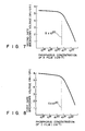
- Fig. 7 graphically shows the relationship between the second gate breakdown voltage of the second insulating film and the phosphorus concentration of the A layer
- Fig. 8 graphically shows the relationship between the first gate breakdown voltage of the first insulating film and the phosphorus concentration of the C layer.
- a high breakdown voltage of the insulating film is maintained when the phosphorus concentration is less than 5 ⁇ 1020 cm ⁇ 3.
- the ordinate denotes the breakdown voltage of second insulating film 56 in terms of the field strength upon the application of a voltage across the first and second poly-Si films
- the abscissa denotes the concentration of phosphorus.
- the open circles show values obtained in accordance with the present invention
- the solid circles represent values obtained in using the conventional method
- a vertical crossing portion shows variations in the breakdown voltage. It is obvious from Fig. 9 that the improvement in the breakdown voltage is due to the manufacturing process of the present invention.
- poly-Si film 55 was thermally oxidized in the second deposition process of the embodiment to provide a second film (silicon oxide film 56), the same effect of the present invention can be obtained by using one of the other two insulating films to form a second film.
Landscapes
- Non-Volatile Memory (AREA)
- Internal Circuitry In Semiconductor Integrated Circuit Devices (AREA)
- Semiconductor Memories (AREA)
- Electrodes Of Semiconductors (AREA)
Applications Claiming Priority (2)
| Application Number | Priority Date | Filing Date | Title |
|---|---|---|---|
| JP89773/87 | 1987-04-14 | ||
| JP62089773A JPS63255972A (ja) | 1987-04-14 | 1987-04-14 | 半導体装置の製造方法 |
Publications (3)
| Publication Number | Publication Date |
|---|---|
| EP0287031A2 true EP0287031A2 (de) | 1988-10-19 |
| EP0287031A3 EP0287031A3 (en) | 1989-09-20 |
| EP0287031B1 EP0287031B1 (de) | 1995-02-01 |
Family
ID=13979997
Family Applications (1)
| Application Number | Title | Priority Date | Filing Date |
|---|---|---|---|
| EP88105805A Expired - Lifetime EP0287031B1 (de) | 1987-04-14 | 1988-04-12 | Hohe Durchbruchspannung aufweisende isolierende Schicht, die zwischen Polysilizium-Schichten liegt |
Country Status (4)
| Country | Link |
|---|---|
| EP (1) | EP0287031B1 (de) |
| JP (1) | JPS63255972A (de) |
| KR (1) | KR910006592B1 (de) |
| DE (1) | DE3852903T2 (de) |
Cited By (7)
| Publication number | Priority date | Publication date | Assignee | Title |
|---|---|---|---|---|
| EP0434383A1 (de) * | 1989-12-20 | 1991-06-26 | Nec Corporation | Gatestruktur eines Halbleiterbauelementes mit darin enthaltener Oxidschicht |
| EP0539184A3 (en) * | 1991-10-24 | 1993-08-11 | Kabushiki Kaisha Toshiba | Non-volatile semiconductor memory |
| EP0542575A3 (en) * | 1991-11-14 | 1993-08-18 | Fujitsu Limited | Method for fabricating a semiconductor memory device having a floating gate with improved insulation film quality |
| EP0529951A3 (en) * | 1991-08-26 | 1993-10-13 | American Telephone And Telegraph Company | Improved dielectrics formed on a deposited semiconductor |
| EP0767489A3 (de) * | 1995-10-02 | 1997-07-02 | Toshiba Kk | Nichtflüchtiger Halbleiterspeicher und Verfahren zur Herstellung |
| GB2353403A (en) * | 1999-03-16 | 2001-02-21 | Nec Corp | Method of manufacturing a semiconductor device |
| US20120119308A1 (en) * | 2009-05-20 | 2012-05-17 | Globalfoundries Inc. | Gate etch optimization through silicon dopant profile change |
Families Citing this family (1)
| Publication number | Priority date | Publication date | Assignee | Title |
|---|---|---|---|---|
| JPS6414968A (en) * | 1987-07-08 | 1989-01-19 | Nec Corp | Formation of gate electrode |
Family Cites Families (2)
| Publication number | Priority date | Publication date | Assignee | Title |
|---|---|---|---|---|
| US4441249A (en) * | 1982-05-26 | 1984-04-10 | Bell Telephone Laboratories, Incorporated | Semiconductor integrated circuit capacitor |
| JPH0638496B2 (ja) * | 1983-06-27 | 1994-05-18 | 日本電気株式会社 | 半導体装置 |
-
1987
- 1987-04-14 JP JP62089773A patent/JPS63255972A/ja active Granted
-
1988
- 1988-04-12 DE DE3852903T patent/DE3852903T2/de not_active Expired - Fee Related
- 1988-04-12 EP EP88105805A patent/EP0287031B1/de not_active Expired - Lifetime
- 1988-04-14 KR KR1019880004263A patent/KR910006592B1/ko not_active Expired
Cited By (13)
| Publication number | Priority date | Publication date | Assignee | Title |
|---|---|---|---|---|
| EP0434383A1 (de) * | 1989-12-20 | 1991-06-26 | Nec Corporation | Gatestruktur eines Halbleiterbauelementes mit darin enthaltener Oxidschicht |
| EP0529951A3 (en) * | 1991-08-26 | 1993-10-13 | American Telephone And Telegraph Company | Improved dielectrics formed on a deposited semiconductor |
| KR100271341B1 (ko) * | 1991-10-24 | 2000-11-01 | 니시무로 타이죠 | 불휘발성 반도체 메모리 및 그 제조 방법 |
| EP0539184A3 (en) * | 1991-10-24 | 1993-08-11 | Kabushiki Kaisha Toshiba | Non-volatile semiconductor memory |
| US5365098A (en) * | 1991-10-24 | 1994-11-15 | Kabushiki Kaisha Toshiba | Non-volatile semiconductor memory having improved erasure characteristics |
| EP0542575A3 (en) * | 1991-11-14 | 1993-08-18 | Fujitsu Limited | Method for fabricating a semiconductor memory device having a floating gate with improved insulation film quality |
| US5497018A (en) * | 1991-11-14 | 1996-03-05 | Fujitsu Limited | Semiconductor memory device having a floating gate with improved insulation film quality |
| EP0767489A3 (de) * | 1995-10-02 | 1997-07-02 | Toshiba Kk | Nichtflüchtiger Halbleiterspeicher und Verfahren zur Herstellung |
| US6303440B1 (en) | 1995-10-02 | 2001-10-16 | Kabushiki Kaisha Toshiba | Nonvolatile semiconductor memory, and method of manufacturing the same |
| GB2353403A (en) * | 1999-03-16 | 2001-02-21 | Nec Corp | Method of manufacturing a semiconductor device |
| GB2353403B (en) * | 1999-03-16 | 2001-07-18 | Nec Corp | Method for manufacturing a semiconductor device |
| US20120119308A1 (en) * | 2009-05-20 | 2012-05-17 | Globalfoundries Inc. | Gate etch optimization through silicon dopant profile change |
| US8390042B2 (en) * | 2009-05-20 | 2013-03-05 | Globalfoundries Inc. | Gate etch optimization through silicon dopant profile change |
Also Published As
| Publication number | Publication date |
|---|---|
| EP0287031A3 (en) | 1989-09-20 |
| JPS63255972A (ja) | 1988-10-24 |
| EP0287031B1 (de) | 1995-02-01 |
| KR880013232A (ko) | 1988-11-30 |
| DE3852903D1 (de) | 1995-03-16 |
| JPH0581193B2 (de) | 1993-11-11 |
| DE3852903T2 (de) | 1995-06-29 |
| KR910006592B1 (ko) | 1991-08-28 |
Similar Documents
| Publication | Publication Date | Title |
|---|---|---|
| EP0034910B1 (de) | Verfahren zur Herstellung einer Halbleitervorrichtung und so hergestellte Vorrichtung | |
| JP2761685B2 (ja) | 半導体装置の製造方法 | |
| US4103415A (en) | Insulated-gate field-effect transistor with self-aligned contact hole to source or drain | |
| GB2128807A (en) | Improvements in or relating to a method for fabricating an MOS device | |
| US4558343A (en) | Semiconductor device having a high resistivity layer in direct contact with a polycrystalline silicon layer of high impurity concentration | |
| EP0589713A2 (de) | Dünnfilm Halbleiteranordnung und Verfahren zur Herstellung | |
| US5237196A (en) | Semiconductor device and method for manufacturing the same | |
| EP0032030B1 (de) | Halbleitervorrichtung und Verfahren zur Herstellung einer Halbleitervorrichtung | |
| JPH0614532B2 (ja) | 多結晶半導体材料中に抵抗体を形成する方法 | |
| US4637128A (en) | Method of producing semiconductor device | |
| US4716451A (en) | Semiconductor device with internal gettering region | |
| IE52791B1 (en) | Semiconductor devices | |
| US4746377A (en) | Semiconductor device with thermally oxidized insulating and arsenic diffusion layers | |
| US4358889A (en) | Process for making a late programming enhanced contact ROM | |
| EP0287031A2 (de) | Hohe Durchbruchspannung aufweisende isolierende Schicht, die zwischen Polysilizium-Schichten liegt | |
| US5753943A (en) | Insulated gate type field effect transistor and method of manufacturing the same | |
| KR910003098B1 (ko) | 반도체 메모리장치 및 그 제조방법 | |
| US6100154A (en) | Using LPCVD silicon nitride cap as a barrier to reduce resistance variations from hydrogen intrusion of high-value polysilicon resistor | |
| JP3001362B2 (ja) | 半導体装置の製造方法 | |
| US4284998A (en) | Junction type field effect transistor with source at oxide-gate interface depth to maximize μ | |
| KR930003859B1 (ko) | 반도체장치의 제조방법 | |
| JP2603088B2 (ja) | 半導体装置 | |
| JPS6129144B2 (de) | ||
| EP0454055B1 (de) | Halbleiteranordnung und Verfahren zur Herstellung | |
| JPH0587992B2 (de) |
Legal Events
| Date | Code | Title | Description |
|---|---|---|---|
| PUAI | Public reference made under article 153(3) epc to a published international application that has entered the european phase |
Free format text: ORIGINAL CODE: 0009012 |
|
| 17P | Request for examination filed |
Effective date: 19880412 |
|
| AK | Designated contracting states |
Kind code of ref document: A2 Designated state(s): DE FR GB |
|
| PUAL | Search report despatched |
Free format text: ORIGINAL CODE: 0009013 |
|
| AK | Designated contracting states |
Kind code of ref document: A3 Designated state(s): DE FR GB |
|
| 17Q | First examination report despatched |
Effective date: 19920827 |
|
| RAP1 | Party data changed (applicant data changed or rights of an application transferred) |
Owner name: TOSHIBA MICRO-ELECTRONICS CORPORATION Owner name: KABUSHIKI KAISHA TOSHIBA |
|
| GRAA | (expected) grant |
Free format text: ORIGINAL CODE: 0009210 |
|
| AK | Designated contracting states |
Kind code of ref document: B1 Designated state(s): DE FR GB |
|
| REF | Corresponds to: |
Ref document number: 3852903 Country of ref document: DE Date of ref document: 19950316 |
|
| ET | Fr: translation filed | ||
| PLBE | No opposition filed within time limit |
Free format text: ORIGINAL CODE: 0009261 |
|
| STAA | Information on the status of an ep patent application or granted ep patent |
Free format text: STATUS: NO OPPOSITION FILED WITHIN TIME LIMIT |
|
| 26N | No opposition filed | ||
| PGFP | Annual fee paid to national office [announced via postgrant information from national office to epo] |
Ref country code: FR Payment date: 19970409 Year of fee payment: 10 |
|
| PGFP | Annual fee paid to national office [announced via postgrant information from national office to epo] |
Ref country code: DE Payment date: 19970418 Year of fee payment: 10 |
|
| PG25 | Lapsed in a contracting state [announced via postgrant information from national office to epo] |
Ref country code: FR Free format text: THE PATENT HAS BEEN ANNULLED BY A DECISION OF A NATIONAL AUTHORITY Effective date: 19980430 |
|
| PG25 | Lapsed in a contracting state [announced via postgrant information from national office to epo] |
Ref country code: DE Free format text: LAPSE BECAUSE OF NON-PAYMENT OF DUE FEES Effective date: 19990202 |
|
| REG | Reference to a national code |
Ref country code: FR Ref legal event code: ST |
|
| REG | Reference to a national code |
Ref country code: GB Ref legal event code: IF02 |
|
| PGFP | Annual fee paid to national office [announced via postgrant information from national office to epo] |
Ref country code: GB Payment date: 20070411 Year of fee payment: 20 |
|
| REG | Reference to a national code |
Ref country code: GB Ref legal event code: PE20 Expiry date: 20080411 |
|
| PG25 | Lapsed in a contracting state [announced via postgrant information from national office to epo] |
Ref country code: GB Free format text: LAPSE BECAUSE OF EXPIRATION OF PROTECTION Effective date: 20080411 |