EP0287383B2 - Supraleitender keramischer Film und Verfahren zu dessen Herstellung - Google Patents
Supraleitender keramischer Film und Verfahren zu dessen Herstellung Download PDFInfo
- Publication number
- EP0287383B2 EP0287383B2 EP88303404A EP88303404A EP0287383B2 EP 0287383 B2 EP0287383 B2 EP 0287383B2 EP 88303404 A EP88303404 A EP 88303404A EP 88303404 A EP88303404 A EP 88303404A EP 0287383 B2 EP0287383 B2 EP 0287383B2
- Authority
- EP
- European Patent Office
- Prior art keywords
- film
- superconductive
- region
- substrate
- doped
- Prior art date
- Legal status (The legal status is an assumption and is not a legal conclusion. Google has not performed a legal analysis and makes no representation as to the accuracy of the status listed.)
- Expired - Lifetime
Links
- 239000000919 ceramic Substances 0.000 title claims description 60
- 238000004519 manufacturing process Methods 0.000 title claims description 7
- 239000000758 substrate Substances 0.000 claims description 29
- 239000012535 impurity Substances 0.000 claims description 27
- 230000000737 periodic effect Effects 0.000 claims description 19
- 238000000034 method Methods 0.000 claims description 17
- 239000010949 copper Substances 0.000 claims description 14
- 238000005468 ion implantation Methods 0.000 claims description 14
- 239000004065 semiconductor Substances 0.000 claims description 13
- QPLDLSVMHZLSFG-UHFFFAOYSA-N Copper oxide Chemical compound [Cu]=O QPLDLSVMHZLSFG-UHFFFAOYSA-N 0.000 claims description 10
- 239000005751 Copper oxide Substances 0.000 claims description 10
- 229910000431 copper oxide Inorganic materials 0.000 claims description 10
- 238000004544 sputter deposition Methods 0.000 claims description 8
- 230000015572 biosynthetic process Effects 0.000 claims description 6
- 239000002019 doping agent Substances 0.000 claims description 6
- 239000000463 material Substances 0.000 claims description 6
- 229910052796 boron Inorganic materials 0.000 claims description 4
- 238000000151 deposition Methods 0.000 claims description 4
- 230000008021 deposition Effects 0.000 claims description 4
- 230000001590 oxidative effect Effects 0.000 claims description 4
- 229910052710 silicon Inorganic materials 0.000 claims description 4
- 229910052782 aluminium Inorganic materials 0.000 claims description 3
- 238000000137 annealing Methods 0.000 claims description 3
- 229910052732 germanium Inorganic materials 0.000 claims description 3
- 229910052742 iron Inorganic materials 0.000 claims description 3
- 229910052698 phosphorus Inorganic materials 0.000 claims description 3
- 229910052719 titanium Inorganic materials 0.000 claims description 3
- 229910052726 zirconium Inorganic materials 0.000 claims description 3
- 229910052759 nickel Inorganic materials 0.000 claims 2
- 238000000059 patterning Methods 0.000 claims 1
- 239000010408 film Substances 0.000 description 69
- IJGRMHOSHXDMSA-UHFFFAOYSA-N Atomic nitrogen Chemical compound N#N IJGRMHOSHXDMSA-UHFFFAOYSA-N 0.000 description 14
- 239000007788 liquid Substances 0.000 description 7
- 229910052757 nitrogen Inorganic materials 0.000 description 7
- 238000010304 firing Methods 0.000 description 6
- 239000011777 magnesium Substances 0.000 description 5
- 229910052749 magnesium Inorganic materials 0.000 description 4
- 238000000206 photolithography Methods 0.000 description 4
- CURLTUGMZLYLDI-UHFFFAOYSA-N Carbon dioxide Chemical compound O=C=O CURLTUGMZLYLDI-UHFFFAOYSA-N 0.000 description 3
- FYYHWMGAXLPEAU-UHFFFAOYSA-N Magnesium Chemical compound [Mg] FYYHWMGAXLPEAU-UHFFFAOYSA-N 0.000 description 3
- XUIMIQQOPSSXEZ-UHFFFAOYSA-N Silicon Chemical compound [Si] XUIMIQQOPSSXEZ-UHFFFAOYSA-N 0.000 description 3
- 229910052784 alkaline earth metal Inorganic materials 0.000 description 3
- 150000001342 alkaline earth metals Chemical class 0.000 description 3
- 229910052790 beryllium Inorganic materials 0.000 description 3
- ATBAMAFKBVZNFJ-UHFFFAOYSA-N beryllium atom Chemical compound [Be] ATBAMAFKBVZNFJ-UHFFFAOYSA-N 0.000 description 3
- 229910052574 oxide ceramic Inorganic materials 0.000 description 3
- 239000011224 oxide ceramic Substances 0.000 description 3
- 239000010703 silicon Substances 0.000 description 3
- 239000010409 thin film Substances 0.000 description 3
- 230000007704 transition Effects 0.000 description 3
- 229910052581 Si3N4 Inorganic materials 0.000 description 2
- VYPSYNLAJGMNEJ-UHFFFAOYSA-N Silicium dioxide Chemical compound O=[Si]=O VYPSYNLAJGMNEJ-UHFFFAOYSA-N 0.000 description 2
- 229910010293 ceramic material Inorganic materials 0.000 description 2
- 239000004020 conductor Substances 0.000 description 2
- 229910052761 rare earth metal Inorganic materials 0.000 description 2
- HQVNEWCFYHHQES-UHFFFAOYSA-N silicon nitride Chemical compound N12[Si]34N5[Si]62N3[Si]51N64 HQVNEWCFYHHQES-UHFFFAOYSA-N 0.000 description 2
- 229910052814 silicon oxide Inorganic materials 0.000 description 2
- 238000005477 sputtering target Methods 0.000 description 2
- 239000002887 superconductor Substances 0.000 description 2
- 238000007669 thermal treatment Methods 0.000 description 2
- 241000272194 Ciconiiformes Species 0.000 description 1
- 229910000750 Niobium-germanium Inorganic materials 0.000 description 1
- 229910002370 SrTiO3 Inorganic materials 0.000 description 1
- VVTSZOCINPYFDP-UHFFFAOYSA-N [O].[Ar] Chemical compound [O].[Ar] VVTSZOCINPYFDP-UHFFFAOYSA-N 0.000 description 1
- 229910052787 antimony Inorganic materials 0.000 description 1
- 229910052785 arsenic Inorganic materials 0.000 description 1
- QVGXLLKOCUKJST-UHFFFAOYSA-N atomic oxygen Chemical compound [O] QVGXLLKOCUKJST-UHFFFAOYSA-N 0.000 description 1
- 229910052797 bismuth Inorganic materials 0.000 description 1
- 239000001569 carbon dioxide Substances 0.000 description 1
- 229910002092 carbon dioxide Inorganic materials 0.000 description 1
- 235000011089 carbon dioxide Nutrition 0.000 description 1
- 229910002106 crystalline ceramic Inorganic materials 0.000 description 1
- 239000011222 crystalline ceramic Substances 0.000 description 1
- 238000010586 diagram Methods 0.000 description 1
- -1 dry ice temperatures Chemical compound 0.000 description 1
- 230000000694 effects Effects 0.000 description 1
- 238000005566 electron beam evaporation Methods 0.000 description 1
- 238000010894 electron beam technology Methods 0.000 description 1
- 229910052733 gallium Inorganic materials 0.000 description 1
- 238000010849 ion bombardment Methods 0.000 description 1
- 150000002500 ions Chemical class 0.000 description 1
- 239000007769 metal material Substances 0.000 description 1
- VUZPPFZMUPKLLV-UHFFFAOYSA-N methane;hydrate Chemical compound C.O VUZPPFZMUPKLLV-UHFFFAOYSA-N 0.000 description 1
- 238000007254 oxidation reaction Methods 0.000 description 1
- 229910052760 oxygen Inorganic materials 0.000 description 1
- 239000001301 oxygen Substances 0.000 description 1
- 229920002120 photoresistant polymer Polymers 0.000 description 1
- 238000005240 physical vapour deposition Methods 0.000 description 1
- 238000002360 preparation method Methods 0.000 description 1
- 230000009466 transformation Effects 0.000 description 1
- XLYOFNOQVPJJNP-UHFFFAOYSA-N water Substances O XLYOFNOQVPJJNP-UHFFFAOYSA-N 0.000 description 1
- 229910052727 yttrium Inorganic materials 0.000 description 1
- VWQVUPCCIRVNHF-UHFFFAOYSA-N yttrium atom Chemical compound [Y] VWQVUPCCIRVNHF-UHFFFAOYSA-N 0.000 description 1
- 229910052845 zircon Inorganic materials 0.000 description 1
- GFQYVLUOOAAOGM-UHFFFAOYSA-N zirconium(iv) silicate Chemical compound [Zr+4].[O-][Si]([O-])([O-])[O-] GFQYVLUOOAAOGM-UHFFFAOYSA-N 0.000 description 1
Images

Classifications
-
- H—ELECTRICITY
- H10—SEMICONDUCTOR DEVICES; ELECTRIC SOLID-STATE DEVICES NOT OTHERWISE PROVIDED FOR
- H10N—ELECTRIC SOLID-STATE DEVICES NOT OTHERWISE PROVIDED FOR
- H10N60/00—Superconducting devices
- H10N60/01—Manufacture or treatment
- H10N60/0268—Manufacture or treatment of devices comprising copper oxide
- H10N60/0661—Processes performed after copper oxide formation, e.g. patterning
-
- H—ELECTRICITY
- H10—SEMICONDUCTOR DEVICES; ELECTRIC SOLID-STATE DEVICES NOT OTHERWISE PROVIDED FOR
- H10N—ELECTRIC SOLID-STATE DEVICES NOT OTHERWISE PROVIDED FOR
- H10N60/00—Superconducting devices
- H10N60/01—Manufacture or treatment
- H10N60/0268—Manufacture or treatment of devices comprising copper oxide
- H10N60/0296—Processes for depositing or forming copper oxide superconductor layers
- H10N60/0381—Processes for depositing or forming copper oxide superconductor layers by evaporation, e.g. MBE
-
- H—ELECTRICITY
- H10—SEMICONDUCTOR DEVICES; ELECTRIC SOLID-STATE DEVICES NOT OTHERWISE PROVIDED FOR
- H10N—ELECTRIC SOLID-STATE DEVICES NOT OTHERWISE PROVIDED FOR
- H10N60/00—Superconducting devices
- H10N60/01—Manufacture or treatment
- H10N60/0268—Manufacture or treatment of devices comprising copper oxide
- H10N60/0296—Processes for depositing or forming copper oxide superconductor layers
- H10N60/0408—Processes for depositing or forming copper oxide superconductor layers by sputtering
-
- H—ELECTRICITY
- H10—SEMICONDUCTOR DEVICES; ELECTRIC SOLID-STATE DEVICES NOT OTHERWISE PROVIDED FOR
- H10N—ELECTRIC SOLID-STATE DEVICES NOT OTHERWISE PROVIDED FOR
- H10N60/00—Superconducting devices
- H10N60/01—Manufacture or treatment
- H10N60/0884—Treatment of superconductor layers by irradiation, e.g. ion-beam, electron-beam, laser beam or X-rays
-
- H—ELECTRICITY
- H10—SEMICONDUCTOR DEVICES; ELECTRIC SOLID-STATE DEVICES NOT OTHERWISE PROVIDED FOR
- H10N—ELECTRIC SOLID-STATE DEVICES NOT OTHERWISE PROVIDED FOR
- H10N60/00—Superconducting devices
- H10N60/01—Manufacture or treatment
- H10N60/0912—Manufacture or treatment of Josephson-effect devices
- H10N60/0941—Manufacture or treatment of Josephson-effect devices comprising high-Tc ceramic materials
-
- H—ELECTRICITY
- H10—SEMICONDUCTOR DEVICES; ELECTRIC SOLID-STATE DEVICES NOT OTHERWISE PROVIDED FOR
- H10N—ELECTRIC SOLID-STATE DEVICES NOT OTHERWISE PROVIDED FOR
- H10N60/00—Superconducting devices
- H10N60/10—Junction-based devices
- H10N60/12—Josephson-effect devices
- H10N60/124—Josephson-effect devices comprising high-Tc ceramic materials
-
- H—ELECTRICITY
- H10—SEMICONDUCTOR DEVICES; ELECTRIC SOLID-STATE DEVICES NOT OTHERWISE PROVIDED FOR
- H10N—ELECTRIC SOLID-STATE DEVICES NOT OTHERWISE PROVIDED FOR
- H10N60/00—Superconducting devices
- H10N60/80—Constructional details
- H10N60/85—Superconducting active materials
- H10N60/855—Ceramic superconductors
- H10N60/857—Ceramic superconductors comprising copper oxide
-
- Y—GENERAL TAGGING OF NEW TECHNOLOGICAL DEVELOPMENTS; GENERAL TAGGING OF CROSS-SECTIONAL TECHNOLOGIES SPANNING OVER SEVERAL SECTIONS OF THE IPC; TECHNICAL SUBJECTS COVERED BY FORMER USPC CROSS-REFERENCE ART COLLECTIONS [XRACs] AND DIGESTS
- Y10—TECHNICAL SUBJECTS COVERED BY FORMER USPC
- Y10S—TECHNICAL SUBJECTS COVERED BY FORMER USPC CROSS-REFERENCE ART COLLECTIONS [XRACs] AND DIGESTS
- Y10S428/00—Stock material or miscellaneous articles
- Y10S428/901—Printed circuit
-
- Y—GENERAL TAGGING OF NEW TECHNOLOGICAL DEVELOPMENTS; GENERAL TAGGING OF CROSS-SECTIONAL TECHNOLOGIES SPANNING OVER SEVERAL SECTIONS OF THE IPC; TECHNICAL SUBJECTS COVERED BY FORMER USPC CROSS-REFERENCE ART COLLECTIONS [XRACs] AND DIGESTS
- Y10—TECHNICAL SUBJECTS COVERED BY FORMER USPC
- Y10S—TECHNICAL SUBJECTS COVERED BY FORMER USPC CROSS-REFERENCE ART COLLECTIONS [XRACs] AND DIGESTS
- Y10S428/00—Stock material or miscellaneous articles
- Y10S428/922—Static electricity metal bleed-off metallic stock
- Y10S428/9265—Special properties
- Y10S428/93—Electric superconducting
-
- Y—GENERAL TAGGING OF NEW TECHNOLOGICAL DEVELOPMENTS; GENERAL TAGGING OF CROSS-SECTIONAL TECHNOLOGIES SPANNING OVER SEVERAL SECTIONS OF THE IPC; TECHNICAL SUBJECTS COVERED BY FORMER USPC CROSS-REFERENCE ART COLLECTIONS [XRACs] AND DIGESTS
- Y10—TECHNICAL SUBJECTS COVERED BY FORMER USPC
- Y10S—TECHNICAL SUBJECTS COVERED BY FORMER USPC CROSS-REFERENCE ART COLLECTIONS [XRACs] AND DIGESTS
- Y10S505/00—Superconductor technology: apparatus, material, process
- Y10S505/70—High TC, above 30 k, superconducting device, article, or structured stock
- Y10S505/701—Coated or thin film device, i.e. active or passive
-
- Y—GENERAL TAGGING OF NEW TECHNOLOGICAL DEVELOPMENTS; GENERAL TAGGING OF CROSS-SECTIONAL TECHNOLOGIES SPANNING OVER SEVERAL SECTIONS OF THE IPC; TECHNICAL SUBJECTS COVERED BY FORMER USPC CROSS-REFERENCE ART COLLECTIONS [XRACs] AND DIGESTS
- Y10—TECHNICAL SUBJECTS COVERED BY FORMER USPC
- Y10S—TECHNICAL SUBJECTS COVERED BY FORMER USPC CROSS-REFERENCE ART COLLECTIONS [XRACs] AND DIGESTS
- Y10S505/00—Superconductor technology: apparatus, material, process
- Y10S505/70—High TC, above 30 k, superconducting device, article, or structured stock
- Y10S505/701—Coated or thin film device, i.e. active or passive
- Y10S505/703—Microelectronic device with superconducting conduction line
-
- Y—GENERAL TAGGING OF NEW TECHNOLOGICAL DEVELOPMENTS; GENERAL TAGGING OF CROSS-SECTIONAL TECHNOLOGIES SPANNING OVER SEVERAL SECTIONS OF THE IPC; TECHNICAL SUBJECTS COVERED BY FORMER USPC CROSS-REFERENCE ART COLLECTIONS [XRACs] AND DIGESTS
- Y10—TECHNICAL SUBJECTS COVERED BY FORMER USPC
- Y10S—TECHNICAL SUBJECTS COVERED BY FORMER USPC CROSS-REFERENCE ART COLLECTIONS [XRACs] AND DIGESTS
- Y10S505/00—Superconductor technology: apparatus, material, process
- Y10S505/70—High TC, above 30 k, superconducting device, article, or structured stock
- Y10S505/706—Contact pads or leads bonded to superconductor
-
- Y—GENERAL TAGGING OF NEW TECHNOLOGICAL DEVELOPMENTS; GENERAL TAGGING OF CROSS-SECTIONAL TECHNOLOGIES SPANNING OVER SEVERAL SECTIONS OF THE IPC; TECHNICAL SUBJECTS COVERED BY FORMER USPC CROSS-REFERENCE ART COLLECTIONS [XRACs] AND DIGESTS
- Y10—TECHNICAL SUBJECTS COVERED BY FORMER USPC
- Y10S—TECHNICAL SUBJECTS COVERED BY FORMER USPC CROSS-REFERENCE ART COLLECTIONS [XRACs] AND DIGESTS
- Y10S505/00—Superconductor technology: apparatus, material, process
- Y10S505/725—Process of making or treating high tc, above 30 k, superconducting shaped material, article, or device
- Y10S505/73—Vacuum treating or coating
-
- Y—GENERAL TAGGING OF NEW TECHNOLOGICAL DEVELOPMENTS; GENERAL TAGGING OF CROSS-SECTIONAL TECHNOLOGIES SPANNING OVER SEVERAL SECTIONS OF THE IPC; TECHNICAL SUBJECTS COVERED BY FORMER USPC CROSS-REFERENCE ART COLLECTIONS [XRACs] AND DIGESTS
- Y10—TECHNICAL SUBJECTS COVERED BY FORMER USPC
- Y10S—TECHNICAL SUBJECTS COVERED BY FORMER USPC CROSS-REFERENCE ART COLLECTIONS [XRACs] AND DIGESTS
- Y10S505/00—Superconductor technology: apparatus, material, process
- Y10S505/725—Process of making or treating high tc, above 30 k, superconducting shaped material, article, or device
- Y10S505/742—Annealing
-
- Y—GENERAL TAGGING OF NEW TECHNOLOGICAL DEVELOPMENTS; GENERAL TAGGING OF CROSS-SECTIONAL TECHNOLOGIES SPANNING OVER SEVERAL SECTIONS OF THE IPC; TECHNICAL SUBJECTS COVERED BY FORMER USPC CROSS-REFERENCE ART COLLECTIONS [XRACs] AND DIGESTS
- Y10—TECHNICAL SUBJECTS COVERED BY FORMER USPC
- Y10T—TECHNICAL SUBJECTS COVERED BY FORMER US CLASSIFICATION
- Y10T428/00—Stock material or miscellaneous articles
- Y10T428/24—Structurally defined web or sheet [e.g., overall dimension, etc.]
- Y10T428/24802—Discontinuous or differential coating, impregnation or bond [e.g., artwork, printing, retouched photograph, etc.]
- Y10T428/24926—Discontinuous or differential coating, impregnation or bond [e.g., artwork, printing, retouched photograph, etc.] including ceramic, glass, porcelain or quartz layer
Definitions
- This invention relates to advances in the field of superconductors, and more particularly relates to superconducting ceramic patterns and to methods of manufacturing the same.
- Nb-Ge metallic material for ex-example, Nb 3 Ge
- Nb 3 Ge for ex-example, Nb 3 Ge
- the application of superconducting materials of this type is limited since a very low temperature is required in order to achieve superconductivity and therefore the running cost is very high.
- ceramic materials which exhibit superconducting properties have become known. However, these have been in bulk (ingot) form and as yet there has been little development of superconducting materials in thin film form.
- semiconductor devices provided with a plurality of elements containing semiconductor integrated circuits within the same substrate are known.
- a device comprising high-Tc a superconductive copper oxide ceramic film formed on a substrate and in which at least one region of the film contains partially oxidated, ion implanted, impurity depant which provides the impurity doped region with an electrical resistivity : temperature characteristic different from that of the non-doped film so that the impurity doped region can exhibit a finite resistivity at a temperature at which the non-doped superconductive ceramic film has zero resistance, there being no ion implantation damage to the crystalline structure of the film in the impurity doped region.
- the invention resides in the realisation that characteristics peculiar to relatively high Tc superconductive copper oxide ceramic films can be utilised to achieve selective lowering of the critical temperature of prescribed portions of the ceramic.
- Tco the temperature at which resistance disappears
- Tc onset the temperature at which a drop in resistivity starts
- the resulting doped portions of the superconducting ceramic have a relatively broad transition temperature region between Tco and Tc onset.
- the portions can be transformed into regions with low Tc which are capable of functioning as resistance regions or active regions when maintained at a temperature equal to the relatively high Tc of the non-doped portions.
- A is one or more elements of Groups IIIa and Vb of the Japanese Periodic Table such as the rare earth elements
- Examples of this general formula are BiSrCaCu 2-3 O 4-10 , Y 0.5 Bi 0.5 Sr 1 Ca 1 Cu 2-3 O 4-10 , YBa 2 Cu 3 O 6-8 , Bi 1 Sr 1 Mg 0.5 Ca 0.5 Cu 2-3 O 4-10 , Bi 0.5 Al 0.5 SrCaCu 2-3 O 4-10 .
- These materials can be formed on a surface by electron beam evaporation, sputtering, photo-enhanced CVD, photo-enhanced PVD, and so forth.
- the present invention provides a method of manufacturing a device comprising a high-Tc superconductive copper oxide ceramic film (2) formed on a substrate (1) and wherein at least one region (11) of the film has an electrical resistivity : temperature characteristic different from that of another region (10) of the film such that the first-mentioned region (11) can exhibit a finite resistivity at a temperature at which the other region (10) has zero resistance, the method comprising forming the superconductive copper oxide ceramic film (2) on the substrate (1), defining said at least one region (11) of the film, and introducing an oxidizable impurity dopant into said at least one region (11) and not into said other region (10), the doping being effected by ion implantation and being followed by thermal annealing of the film (2) in an oxidizing atmosphere to cause the dopant to be partially oxidated in the film and to make good any ion implantation damage to the crystalline structure of the film in the impurity doped region, whereby to achieve the required electrical resistivity : temperature
- the invention provides a method wherein a high-Tc superconducting copper oxide ceramic film is deposited on an insulating surface for example by sputtering to produce a film 0.1 to 30 microns in thickness. Prescribed portions of the film are then removed by photolithography to leave masked areas of superconducting ceramic which may subsequently be formed into active devices such as Josephson devices and passive devices such as resistors or conductors (wiring). The masked areas are then processed to selectivly remove the mask from prescribed portions that are destined to be low Tc regions and ion implantation with impurities selected to be partially oxidated in the film is effected through the openings in the remaining mask to produce low Tc regions in the ceramic film at the prescribed portions. After ion implantation, the superconducting film is subjected to thermal treatment to make good any damage to the crystalline structure caused during ion bombardment and to remove the remaining mask.
- Groups la, Ila, VIII, Ib, IIb and 0 are the same in the Japanese and European Periodic Tables
- Groups IIIa, IVa, Va, VIa and VIIa of the Japanese Periodic Table correspond respectively to Groups IIIb, IVb, Vb, VIb and VIIb of the European Periodic Table
- Groups IIIb, IVb, Vb, VIb and VIIb of the Japanese Periodic Table correspond respectively to Groups IIIa, IVa, Va, VIa and VIIa of the European Periodic Table.
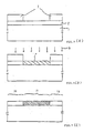
- a method of manufacturing a superconducting ceramic pattern in accordance with the present invention will be described.
- an oxide ceramic thin film 2 of 0.1 to 1.0 ⁇ m (microns) in thickness is deposited by low frequency sputtering onto an insulating single crystalline substrate 1 made of for example SrTiO 3 .
- a sputtering target is chosen whose composition is such that a deposited complex oxide film can be grown which conforms to the stoichiometric formula (YBa 2 )Cu 3 O 6-8 , and the substrate is heated in an argon-oxygen atmosphere at 700 to 1000°C, e.g. 850°C, during the sputtering process.
- impurities such as silicon in the deposited ceramic thin film 2 and it is important that the presence of such impurities is minimised since controlled levels of impurities are added to selected portions of the film in a subsequent stage of the process in order to achieve the desired effect.
- the presence of impurities can be kept below an acceptable level of 100ppm and preferably not more than 10ppm.
- the structure is fired at 800 to 1000°C for 5-50 hours in an oxidizing atmosphere in order to transform the ceramic film into a superconducting single crystalline ceramic film.
- selected portions of the superconducting ceramic film 2 are covered with a photo resist mask 3 so that other unmasked portions of the film 2 can be doped with silicon by ion implantation as shown in Fig.1(B).
- the impurity density of the thus doped portion is 5 ⁇ 10 15 to 2 ⁇ 10 22 atom/cm 3 , e.g. 5 ⁇ 10 19 atom/cm 3 .
- the ceramic film 2 is fired again at a temperature of from 700 to 1000°C in an oxidizing atmosphere.
- This thermal treatment causes oxidization of impurities in the ceramic material and therefore lowers its Tc, and at the same the resist 3 is removed from the ceramic film in the form of carbon dioxide and water.
- Some of the silicon implanted in the ceramic film is oxidized so that the doped portions 11 as shown in Fig.1(C) of the superconducting ceramic come to contain about 0.1% silicon oxide.
- the doped portion 11 of the superconducting ceramic film still contains about 99% of the original ceramic composition (i.e. 99% purity compared to that of the undoped portion 10).
- a curve 20 in Fig.3 plotted in accordance with experimentally obtained data shows the temperature resistivity relationship of the fired undoped ceramic film 10, with temperature points Tco 22 at which the resistivity vanishes and Tc onset 21 at which the resistivity starts to drop sharply.
- Figure 3 also shows how the resistivity-temperature relationship of the doped portions 11 of the superconducting ceramic film changes from the curve 20 to a curve 20' as a result of the doping process.
- Tco of the doped portion 11 shifts to a lower temperature 22' while Tc onset 21' does not change substantially.
- the difference between Tc onset and Tco increases to create a broader transition region 23'.
- the temperature of liquid nitrogen indicated at 25 lies within the transition region 23' and the doped portion 11 therefore has a definite resistivity 26 at the liquid nitrogen temperature 25.
- the change in critical temperature of the doped portion 11 can be controlled by adjusting the amount of the doping and it has been found that the relatively low Tco of the doped portion 11 is not altered even after being subjected to a high temperature of 700 to 1000°C during the subsequent firing process.
- Examples of other impurities which may be added to superconducting complex oxide ceramics in order to achieve the desired drop in Tco include Al, Mg, Ga, Ge, Ti, Zr, Fe, Hi, Co, B and P, and it is also possible to use a plurality of such impurities in combination to achieve the desired result.
- the doping level should be chosen to be higher than the level already occurring in the ceramic film, or alternatively an impurity that does not occur in the film may be added to the film in a suitable quantity to achieve the desired result.
- Transistors and/or other devices are formed in advance within a semiconductor substrate 1.
- a first insulating film 6 is then formed in a predetermined pattern on the upper surface of the substrate 1.
- the insulating film 6 consists of an underlying film 8 made of silicon oxide and an overlying film 9 made of silicon nitride.
- a superconducting complex oxide ceramic film is deposited on the substrate 1 over the insulating film 6 by sputtering and the deposited film is patterned by photolithography as described hereinabove in relation to the foregoing embodiment. Prescribed portions of the ceramic film are then doped with impurities by ion implantation in the same way as explained above to produce superconducting conductor areas 10 and 10' and low Tc regions 11 which can be selectively used as resistances or active regions at the temperature of liquid nitrogen.
- the ceramic film is subjected to lower temperatures than in the preceding embodiment during firing after ion implantation so that the final superconducting ceramic pattern has a polycrystalline structure.
- the devices within the semiconductor substrate co-operate with the superconducting ceramic film by virtue of being interconnected by the superconducting circuit.
- the manufacturing conditions of the superconducting film are selected so that at the temperature of liquid nitrogen the doped regions have a definite resistivity and the non-doped regions are superconducting.
- a second insulating film 9' is formed on the substrate 1 over the films previously deposited thereon together with another insulating film 12 which fills the depressions formed by preceding deposition thereby providing an even upper surface.
- Openings 7' are formed in the insulating films 9' and 12 by photolithography and a second supeconducting ceramic film 13 is deposited over the insulating films 9' and 12 using the same process as in the first embodiment so that the first and the second superconducting ceramic films interconnect through the openings 7'.
- the second superconducting ceramic film 13 is then patterned by photolithography.
- the ceramic film may then be transformed into the desired superconducting film by firing and ion implantation may then be effected.
- the structure of the ceramic film may be altered by ion implantation prior to the firing transformation. In this case, the formation of low Tc regions and high Tc regions is completed after the firing.
- the doped region of the superconducting ceramic film retains many superconducting properties at the liquid nitrogen operating temperature
- the invention is also intended to include a superconducting ceramic consisting of regions which have been doped so heavily that the superconducting properties of the said regions are effectively destroyed.
- a semiconductor substrate provided with active devices therein is utilised
- a ceramic substrate coated with a non-oxide film such as of 50 to 500 x 10 -10 m ( ⁇ ) thick silicon nitride on its upper surface may instead be used.
- a YSZ (yttrium stabilized zircon) substrate may be used which has a coefficient of thermal expansion substantially the same as that of the ceramic.
- A is one or more elements of Group Illa of the Japanese Periodic Table, e.g. the rare earth elements
- B is one or more elements of Group Ila of the Japanese Periodic Table, e.g. the alkaline earth metals including beryllium and magnesium, and 0 ⁇ x ⁇ 1
- y 2.0-4.0, preferably
- A is one or more elements of Group Vb of the Japanese Periodic Table such as Bi, Sb and As
- Examples of this general formula are BiSrCaCuCu 2 O x and Bi 4 Sr 3 Ca 3 Cu 4 O x .
- Tc onset and Tco for certain samples confirmed consistent with the formula Bi 4 Sr y Ca 3 Cu 4 O x (y around 1.5) were measured to be 40-60 K, which is not particularly high.
- Relatively high critical temperatures were obtained with samples conforming to the stoichiometric formulae Bi 4 Sr 4 Ca 2 Cu 4 O x and Bi 2 Sr 3 Ca 2 Cu 2 O x .
- the number x designating the oxygen proportion being of the order of 6-10, e.g. around 8.1.
Landscapes
- Engineering & Computer Science (AREA)
- Manufacturing & Machinery (AREA)
- Chemical & Material Sciences (AREA)
- Ceramic Engineering (AREA)
- Physics & Mathematics (AREA)
- Optics & Photonics (AREA)
- Superconductor Devices And Manufacturing Methods Thereof (AREA)
- Superconductors And Manufacturing Methods Therefor (AREA)
- Inorganic Compounds Of Heavy Metals (AREA)
Claims (18)
- Vorrichtung mit einem auf einem Substrat (1) ausgebildeten, hoch-Tc-supraleitenden, Kupferoxid-Keramikfilm (2), bei der mindestens ein Bereich (11) des Films (2) eine teilweise oxidierte, ionenimplantierte Fremdstoffdotierung enthält, die einen Fremdstoff-dotierten Bereich mit einer Charakteristik elektrischer Widerstand : Temperatur ergibt, die sich von der des undotierten Films unterscheidet, so daß der Fremdstoffdotierte Bereich (11) bei einer Temperatur, bei der der undotierte, supraleitende Keramikfilm (2) keinen Widerstand aufweist, einen endlichen Widerstand aufweisen kann, wobei es in dem Fremdstoff-dotierten Bereich keine Ionenimplantationsschäden an der Kristallstruktur des Films gibt.
- Vorrichtung nach Anspruch 1, bei der die Dotierung des Bereichs (11) eine solche ist, daß dieser seine supraleitende Eigenschaft beibehält, jedoch mit verringerter Tco im Vergleich zum undotierten Film.
- Vorrichtung nach Anspruch 2, bei der die Einsatztemperatur Tc für den dotierten Bereich (11) im Vergleich zu der des undotierten Films im wesentlichen unverändert ist.
- Vorrichtung nach einem der vorstehenden Ansprüche, bei der das Substrat (1) ein Halbleitersubstrat aufweist.
- Vorrichtung nach Anspruch 4, bei der das Halbleitersubstrat (1) Halbleiterbauelemente enthält, die durch ein supraleitendes Schaltungssystem miteinander verbunden sind, wie es im supraleitenden Keramikfilm (2) festgelegt ist.
- Vorrichtung nach Anspruch 5, bei der das im supraleitenden Keramikfilm (2) festgelegte Schaltungssystem mindestens einen durch einen dotierten Bereich (11) des Films (2) gebildeten Widerstand aufweist.
- Vorrichtung nach einem der vorstehenden Ansprüche, bei der der supraleitende Keramikfilm der stöchiometrischen Formel (A1-xBx)yCuzOw genügt, wobei A eines oder mehrere Elemente der Gruppe IIIa und/oder Vb des japanischen Periodensystems aufweist und B eines oder mehrere Elemente der Gruppe IIa des japanischen Periodensystems aufweist.
- Vorrichtung nach einem der vorstehenden Ansprüche, bei der der Fremdstoff eine oder mehrere der Substanzen Si, Al, Mg, Ga, Ge, Ti, Zr, Fe, Ni, Co, B und P umfaßt.
- Vorrichtung nach einem der vorstehenden Ansprüche, bei der die Fremdstoffdichte des Dotierstoffs von 5 x 10¹⁵ bis 2 x 10²² Atome/cm3 reicht.
- Verfahren zum Herstellen einer Vorrichtung mit einem auf einem Substrat (1) ausgebildeten hoch-Tc-supraleitenden Kupferoxid-Keramikfilm (2), wobei mindestens ein Bereich (11) des Films eine Charakteristik elektrischer Widerstand : Temperatur aufweist, die sich von der eines anderen Bereichs (10) des Films in solcher Weise unterscheidet, daß der erstgenannte Bereich (11) bei einer Temperatur, bei der der andere Bereich (10) keinen Widerstand aufweist, einen endlichen Widerstand aufweisen kann, welches Verfahren es umfaßt, den supraleitenden Kupferoxid-Keramikfilm (2) auf dem Substrat (1) auszubilden, den mindestens einen Bereich (11) auf dem Film festzulegen und eine oxidierbare Fremdstoffdotierung in den mindestens einen Bereich (11) und nicht in den anderen Bereich (10) einzubringen, wobei die Dotierung durch Ionenimplantation bewirkt wird, dem thermisches Tempern des Films (2) in einer oxidierenden Atmosphäre folgt, um die Dotierung teilweise in dem Film zu oxidieren und um irgendeinen Ionenimplantationsschaden an der Kristallstruktur des Films in dem Fremdstoff-dotierten Bereich auszugleichen, um dadurch die erforderliche Charakteristik elektrischer Widerstand : Temperatur zu erzielen.
- Verfahren nach Anspruch 10, bei dem zum Ausbilden des supraleitenden Karamikfilms (2) auf dem Substrat (1) das Sputtern eines Materials auf das Substrat gehört, das eine Zusammensetzung aufweist, die für die Ausbildung eines supraleitenden Films geeignet ist.
- Verfahren nach Anspruch 10, bei dem zur Ausbildung des supraleitenden Keramikfilms (2) auf dem Substrat (1) das Abscheiden eines Materials mit einer Zusammensetzung, die für das Ausbilden eines supraleitenden Films auf dem Substrat geeignet ist, durch Drucken, durch MBE-Wachstum oder aus der Gasphase gehört.
- Verfahren nach einem der Ansprüche 10, 11 oder 12, bei dem der auf dem Substrat auszubildende Film gemustert wird, um aktive und/oder passive supraleitende Bauelemente festzulegen.
- Verfahren nach Anspruch 13, bei dem das Substrat (1) ein Halbleitersubstrat mit einem oder mehreren in diesem ausgebildeten Halbleiterbauelementen aufweist, und das Mustern des supraleitenden Films (2) ausgeführt wird, um aktive und/oder passive supraleitende Bauelemente festzulegen, die so ausgebildet sind, daß sie mit dem einen oder mehreren Halbleiterbauelementen wechselwirken.
- Verfahren nach einem der Ansprüche 10 bis 14, bei dem der supraleitende Keramikfilm der stöchiometrischen Formel (A1-xBx)yCuzOw genügt, wobei A eines oder mehrere Elemente der Gruppe IIIa und/oder Vb des japanischen Periodensystems aufweist und B eines oder mehrere Elemente der Gruppe IIa des japanischen Periodensystems aufweist.
- Verfahren nach einem der Ansprüche 10 bis 15, bei dem zum Fremdstoff einer oder mehrere der Stoffe Si, Al, Mg, Ga, Ge, Ti, Zr, Fe, Ni, Co, B und P gehört.
- Verfahren nach einem der Ansprüche 10 bis 16, bei dem das Dotieren des mindestens einen Bereichs (11) des supraleitenden Keramikfilms so ausgeführt wird, daß in diesem dotierten Bereich (11) nichtsupraleitende Eigenschaften erhalten werden.
- Verfahren nach einem der Ansprüche 10 bis 16, bei dem das Dotieren des mindestens einen Bereichs (11) des supraleitenden Keramikfilms so ausgeführt wird, daß die dotierten und die undotierten Bereiche des Films Supraleitungseigenschaften aufweisen, daß jedoch der dotierte Bereich eine tiefere Tco als der undotierte Bereich aufweist.
Applications Claiming Priority (6)
| Application Number | Priority Date | Filing Date | Title |
|---|---|---|---|
| JP62093732A JP2670554B2 (ja) | 1987-04-15 | 1987-04-15 | 酸化物超電導材料の作製方法 |
| JP93733/87 | 1987-04-15 | ||
| JP93732/87 | 1987-04-15 | ||
| JP9373387 | 1987-04-15 | ||
| JP62093733A JPS63258083A (ja) | 1987-04-15 | 1987-04-15 | 超電導材料の作製方法 |
| JP9373287 | 1987-04-15 |
Publications (4)
| Publication Number | Publication Date |
|---|---|
| EP0287383A2 EP0287383A2 (de) | 1988-10-19 |
| EP0287383A3 EP0287383A3 (en) | 1989-04-05 |
| EP0287383B1 EP0287383B1 (de) | 1993-03-24 |
| EP0287383B2 true EP0287383B2 (de) | 2002-08-21 |
Family
ID=26435026
Family Applications (1)
| Application Number | Title | Priority Date | Filing Date |
|---|---|---|---|
| EP88303404A Expired - Lifetime EP0287383B2 (de) | 1987-04-15 | 1988-04-15 | Supraleitender keramischer Film und Verfahren zu dessen Herstellung |
Country Status (6)
| Country | Link |
|---|---|
| US (2) | US5098884A (de) |
| EP (1) | EP0287383B2 (de) |
| KR (1) | KR910004994B1 (de) |
| CN (1) | CN1018115B (de) |
| AU (1) | AU599223B2 (de) |
| DE (1) | DE3879536T3 (de) |
Families Citing this family (16)
| Publication number | Priority date | Publication date | Assignee | Title |
|---|---|---|---|---|
| US5248658A (en) * | 1987-04-07 | 1993-09-28 | Semiconductor Energy Laboratory Co., Ltd. | Method of manufacturing a superconducting oxide pattern by laser sublimation |
| US5401716A (en) * | 1987-04-15 | 1995-03-28 | Semiconductor Energy Laboratory Co., Ltd. | Method for manufacturing superconducting patterns |
| AU599223B2 (en) * | 1987-04-15 | 1990-07-12 | Semiconductor Energy Laboratory Co. Ltd. | Superconducting ceramic pattern and its manufacturing method |
| US4900716A (en) * | 1987-05-18 | 1990-02-13 | Sumitomo Electric Industries, Ltd. | Process for producing a compound oxide type superconducting material |
| US5225394A (en) * | 1987-08-31 | 1993-07-06 | Semiconductor Energy Laboratory Co., Ltd. | Method for manufacturing high Tc superconducting circuits |
| FR2641530B2 (fr) * | 1988-01-29 | 1993-05-28 | Centre Nat Rech Scient | Nouveau materiau composite, procede de fabrication et application |
| EP0358879A3 (de) * | 1988-09-13 | 1991-02-27 | Hewlett-Packard Company | Verfahren zur Herstellung hochintegrierter Verbindungen |
| JPH06291374A (ja) * | 1993-03-31 | 1994-10-18 | Sumitomo Electric Ind Ltd | ジョセフソン接合素子 |
| AU6674794A (en) * | 1993-05-14 | 1994-12-12 | University Of British Columbia, The | Fabrication of oxide superconductor devices by impurity ion implantation |
| JPH07263767A (ja) | 1994-01-14 | 1995-10-13 | Trw Inc | イオンインプランテーションを用いたプレーナ型の高温超伝導集積回路 |
| US5912503A (en) * | 1997-01-02 | 1999-06-15 | Trw Inc. | Planar in-line resistors for superconductor circuits |
| US7247603B2 (en) * | 2003-10-23 | 2007-07-24 | Star Cryoelectronics | Charge dissipative dielectric for cryogenic devices |
| KR100595855B1 (ko) * | 2004-12-29 | 2006-06-30 | 동부일렉트로닉스 주식회사 | 알루미늄 증착 콘택트 형성 방법 |
| US7615385B2 (en) | 2006-09-20 | 2009-11-10 | Hypres, Inc | Double-masking technique for increasing fabrication yield in superconducting electronics |
| CN102437281A (zh) * | 2011-12-08 | 2012-05-02 | 南京大学 | 一种超导隧道结及其制备方法 |
| CN111063788B (zh) * | 2019-11-27 | 2022-06-07 | 中国科学院上海微系统与信息技术研究所 | 一种超导转变边探测器的制备方法 |
Family Cites Families (13)
| Publication number | Priority date | Publication date | Assignee | Title |
|---|---|---|---|---|
| US3346425A (en) * | 1964-04-01 | 1967-10-10 | Gen Electric | Superconductors |
| US4316785A (en) * | 1979-11-05 | 1982-02-23 | Nippon Telegraph & Telephone Public Corporation | Oxide superconductor Josephson junction and fabrication method therefor |
| JPS58122724A (ja) * | 1982-01-18 | 1983-07-21 | Toshiba Corp | 半導体素子の製造方法 |
| JPS61191070A (ja) * | 1985-02-20 | 1986-08-25 | Toshiba Corp | 半導体装置の製造方法 |
| JPS6215864A (ja) * | 1985-07-15 | 1987-01-24 | Hitachi Ltd | 太陽電池の製造方法 |
| US4732867A (en) * | 1986-11-03 | 1988-03-22 | General Electric Company | Method of forming alignment marks in sapphire |
| US4826808A (en) * | 1987-03-27 | 1989-05-02 | Massachusetts Institute Of Technology | Preparation of superconducting oxides and oxide-metal composites |
| US4960751A (en) * | 1987-04-01 | 1990-10-02 | Semiconductor Energy Laboratory Co., Ltd. | Electric circuit having superconducting multilayered structure and manufacturing method for same |
| AU599223B2 (en) * | 1987-04-15 | 1990-07-12 | Semiconductor Energy Laboratory Co. Ltd. | Superconducting ceramic pattern and its manufacturing method |
| CA1328242C (en) * | 1987-05-18 | 1994-04-05 | Nobuhiko Fujita | Process for manufacturing a superconductor and a method for producing a superconducting circuit |
| US4837609A (en) * | 1987-09-09 | 1989-06-06 | American Telephone And Telegraph Company, At&T Bell Laboratories | Semiconductor devices having superconducting interconnects |
| JPH01290526A (ja) * | 1988-05-18 | 1989-11-22 | Seiko Epson Corp | 高温超電導材料 |
| DE69219816T2 (de) * | 1991-03-11 | 1997-10-23 | Sumitomo Electric Industries | Supraleitende Dünnschicht mit mindestens einer isolierten Region, gebildet aus oxydisch supraleitendem Material und Verfahren zu ihrer Herstellung |
-
1988
- 1988-04-13 AU AU14573/88A patent/AU599223B2/en not_active Ceased
- 1988-04-15 EP EP88303404A patent/EP0287383B2/de not_active Expired - Lifetime
- 1988-04-15 CN CN88102320A patent/CN1018115B/zh not_active Expired
- 1988-04-15 KR KR1019880004307A patent/KR910004994B1/ko not_active Expired
- 1988-04-15 DE DE3879536T patent/DE3879536T3/de not_active Expired - Lifetime
-
1990
- 1990-03-05 US US07/488,252 patent/US5098884A/en not_active Expired - Lifetime
-
1995
- 1995-05-17 US US08/443,170 patent/US5877124A/en not_active Expired - Fee Related
Also Published As
| Publication number | Publication date |
|---|---|
| DE3879536D1 (de) | 1993-04-29 |
| EP0287383B1 (de) | 1993-03-24 |
| AU1457388A (en) | 1988-10-20 |
| US5098884A (en) | 1992-03-24 |
| CN1018115B (zh) | 1992-09-02 |
| DE3879536T3 (de) | 2003-07-24 |
| AU599223B2 (en) | 1990-07-12 |
| DE3879536T2 (de) | 1993-07-01 |
| KR880013190A (ko) | 1988-11-30 |
| US5877124A (en) | 1999-03-02 |
| EP0287383A2 (de) | 1988-10-19 |
| EP0287383A3 (en) | 1989-04-05 |
| CN88102320A (zh) | 1988-11-02 |
| KR910004994B1 (ko) | 1991-07-20 |
Similar Documents
| Publication | Publication Date | Title |
|---|---|---|
| EP0287383B2 (de) | Supraleitender keramischer Film und Verfahren zu dessen Herstellung | |
| EP0364101B1 (de) | Methode zur Bildung eines Schwach-Kopplungs-Josephson-Übergangs und supraleitende Einrichtung, welche diesen Übergang benutzt | |
| US5051396A (en) | Method of manufacturing superconducting patterns by adding impurities | |
| EP0660968A1 (de) | Verbesserte sperrschichten fuer oxid-supraleiter-anordnungen und schaltungen | |
| US5215960A (en) | Method for manufacturing oxide superconducting devices | |
| EP0327493B1 (de) | Epitaxische Anordnung von Hochtemperatur-Supraleitern | |
| US5512540A (en) | Method of manufacturing superconducting patterns | |
| EP0341148B1 (de) | Halbleitersubstrat mit dünner Supraleiterschicht | |
| US5982034A (en) | Conductive oxide films | |
| EP0508844B1 (de) | Supraleitende Dünnschicht mit mindestens einer isolierten Region, gebildet aus oxydisch supraleitendem Material und Verfahren zu ihrer Herstellung | |
| KR940003745B1 (ko) | 산화물 초전도체를 갖는 능동소자 및 그의 제조방법 | |
| JPH0577312B2 (de) | ||
| JP2670554B2 (ja) | 酸化物超電導材料の作製方法 | |
| JP3425422B2 (ja) | 超電導素子の製造方法 | |
| JP2544390B2 (ja) | 酸化物超電導集積回路 | |
| JPS63258083A (ja) | 超電導材料の作製方法 | |
| KR930004024B1 (ko) | 초전도 집적회로소자의 제조방법 | |
| EP0510201B1 (de) | Verfahren zur herstellung einer dünnen supraleitenden schicht | |
| JPS63250882A (ja) | 酸化物超電導材料の絶縁化方法 | |
| JP2559413B2 (ja) | 酸化物超電導集積回路 | |
| Kawabata et al. | Fabrication of YBa 2 Cu 3 O 7< cd0215d. gif> x-PrBa 2 Cu 3 O 7< cd0215d. gif> y Hetero-Structure by Using a Hollow Cathode Discharge Sputtering System | |
| EP0471292A2 (de) | Substrat für supraleitende Einrichtungen | |
| JP3323278B2 (ja) | 超電導デバイスの製造方法 | |
| EP0545777A2 (de) | Verfahren zum Herstellen einer supraleitenden Dünnschicht mit einer Stelle reduzierter Schichtdicke und supraleitendes Bauelement, das eine derartige supraleitende Dünnschicht enthält | |
| JPH0577311B2 (de) |
Legal Events
| Date | Code | Title | Description |
|---|---|---|---|
| PUAI | Public reference made under article 153(3) epc to a published international application that has entered the european phase |
Free format text: ORIGINAL CODE: 0009012 |
|
| AK | Designated contracting states |
Kind code of ref document: A2 Designated state(s): DE FR GB |
|
| PUAL | Search report despatched |
Free format text: ORIGINAL CODE: 0009013 |
|
| AK | Designated contracting states |
Kind code of ref document: A3 Designated state(s): DE FR GB |
|
| 17P | Request for examination filed |
Effective date: 19890516 |
|
| 17Q | First examination report despatched |
Effective date: 19900404 |
|
| GRAA | (expected) grant |
Free format text: ORIGINAL CODE: 0009210 |
|
| AK | Designated contracting states |
Kind code of ref document: B1 Designated state(s): DE FR GB |
|
| REF | Corresponds to: |
Ref document number: 3879536 Country of ref document: DE Date of ref document: 19930429 |
|
| ET | Fr: translation filed | ||
| PLBI | Opposition filed |
Free format text: ORIGINAL CODE: 0009260 |
|
| 26 | Opposition filed |
Opponent name: SIEMENS AG Effective date: 19931217 |
|
| PLAW | Interlocutory decision in opposition |
Free format text: ORIGINAL CODE: EPIDOS IDOP |
|
| APAA | Appeal reference recorded |
Free format text: ORIGINAL CODE: EPIDOS REFN |
|
| APAC | Appeal dossier modified |
Free format text: ORIGINAL CODE: EPIDOS NOAPO |
|
| APAC | Appeal dossier modified |
Free format text: ORIGINAL CODE: EPIDOS NOAPO |
|
| APAE | Appeal reference modified |
Free format text: ORIGINAL CODE: EPIDOS REFNO |
|
| APAC | Appeal dossier modified |
Free format text: ORIGINAL CODE: EPIDOS NOAPO |
|
| PLAW | Interlocutory decision in opposition |
Free format text: ORIGINAL CODE: EPIDOS IDOP |
|
| PLAW | Interlocutory decision in opposition |
Free format text: ORIGINAL CODE: EPIDOS IDOP |
|
| PLAW | Interlocutory decision in opposition |
Free format text: ORIGINAL CODE: EPIDOS IDOP |
|
| REG | Reference to a national code |
Ref country code: GB Ref legal event code: IF02 |
|
| PLAW | Interlocutory decision in opposition |
Free format text: ORIGINAL CODE: EPIDOS IDOP |
|
| PUAH | Patent maintained in amended form |
Free format text: ORIGINAL CODE: 0009272 |
|
| STAA | Information on the status of an ep patent application or granted ep patent |
Free format text: STATUS: PATENT MAINTAINED AS AMENDED |
|
| 27A | Patent maintained in amended form |
Effective date: 20020821 |
|
| AK | Designated contracting states |
Kind code of ref document: B2 Designated state(s): DE FR GB |
|
| ET3 | Fr: translation filed ** decision concerning opposition | ||
| PGFP | Annual fee paid to national office [announced via postgrant information from national office to epo] |
Ref country code: FR Payment date: 20030408 Year of fee payment: 16 |
|
| PGFP | Annual fee paid to national office [announced via postgrant information from national office to epo] |
Ref country code: GB Payment date: 20030409 Year of fee payment: 16 |
|
| PG25 | Lapsed in a contracting state [announced via postgrant information from national office to epo] |
Ref country code: GB Free format text: LAPSE BECAUSE OF NON-PAYMENT OF DUE FEES Effective date: 20040415 |
|
| GBPC | Gb: european patent ceased through non-payment of renewal fee |
Effective date: 20040415 |
|
| PG25 | Lapsed in a contracting state [announced via postgrant information from national office to epo] |
Ref country code: FR Free format text: LAPSE BECAUSE OF NON-PAYMENT OF DUE FEES Effective date: 20041231 |
|
| REG | Reference to a national code |
Ref country code: FR Ref legal event code: ST |
|
| APAH | Appeal reference modified |
Free format text: ORIGINAL CODE: EPIDOSCREFNO |
|
| PGFP | Annual fee paid to national office [announced via postgrant information from national office to epo] |
Ref country code: DE Payment date: 20070412 Year of fee payment: 20 |