EP0287843B1 - Procédé de fabrication de plaques de circuits imprimés - Google Patents
Procédé de fabrication de plaques de circuits imprimés Download PDFInfo
- Publication number
- EP0287843B1 EP0287843B1 EP88104882A EP88104882A EP0287843B1 EP 0287843 B1 EP0287843 B1 EP 0287843B1 EP 88104882 A EP88104882 A EP 88104882A EP 88104882 A EP88104882 A EP 88104882A EP 0287843 B1 EP0287843 B1 EP 0287843B1
- Authority
- EP
- European Patent Office
- Prior art keywords
- ablation
- process according
- nucleation
- substrate
- circuit boards
- Prior art date
- Legal status (The legal status is an assumption and is not a legal conclusion. Google has not performed a legal analysis and makes no representation as to the accuracy of the status listed.)
- Expired - Lifetime
Links
- 238000000034 method Methods 0.000 title claims abstract description 21
- 238000004519 manufacturing process Methods 0.000 title claims abstract description 11
- 230000008569 process Effects 0.000 title claims description 10
- 239000004020 conductor Substances 0.000 claims abstract description 24
- 238000002679 ablation Methods 0.000 claims abstract description 20
- 239000000758 substrate Substances 0.000 claims abstract description 20
- 238000010899 nucleation Methods 0.000 claims abstract description 12
- 238000005516 engineering process Methods 0.000 claims abstract description 11
- 239000000654 additive Substances 0.000 claims abstract description 10
- 230000006911 nucleation Effects 0.000 claims abstract description 10
- 230000000996 additive effect Effects 0.000 claims abstract description 9
- 230000005670 electromagnetic radiation Effects 0.000 claims abstract description 9
- 239000000463 material Substances 0.000 claims abstract description 8
- 229910052751 metal Inorganic materials 0.000 claims description 10
- 239000002184 metal Substances 0.000 claims description 10
- 239000004697 Polyetherimide Substances 0.000 claims description 5
- 229920001601 polyetherimide Polymers 0.000 claims description 5
- 230000004913 activation Effects 0.000 claims description 4
- 238000000151 deposition Methods 0.000 claims 4
- 230000008021 deposition Effects 0.000 claims 4
- 238000004070 electrodeposition Methods 0.000 claims 2
- 229910021626 Tin(II) chloride Inorganic materials 0.000 claims 1
- 239000011248 coating agent Substances 0.000 claims 1
- 238000000576 coating method Methods 0.000 claims 1
- 150000001875 compounds Chemical class 0.000 claims 1
- 239000000835 fiber Substances 0.000 claims 1
- 238000001465 metallisation Methods 0.000 abstract description 7
- 239000000126 substance Substances 0.000 abstract description 4
- 239000011229 interlayer Substances 0.000 abstract 1
- 239000010410 layer Substances 0.000 abstract 1
- 230000035784 germination Effects 0.000 description 16
- RYGMFSIKBFXOCR-UHFFFAOYSA-N Copper Chemical compound [Cu] RYGMFSIKBFXOCR-UHFFFAOYSA-N 0.000 description 7
- 230000005540 biological transmission Effects 0.000 description 7
- 229910052802 copper Inorganic materials 0.000 description 7
- 239000010949 copper Substances 0.000 description 7
- 230000008901 benefit Effects 0.000 description 3
- 238000010586 diagram Methods 0.000 description 3
- 150000002941 palladium compounds Chemical class 0.000 description 3
- 238000005554 pickling Methods 0.000 description 3
- 230000001133 acceleration Effects 0.000 description 2
- 230000003213 activating effect Effects 0.000 description 2
- 239000002318 adhesion promoter Substances 0.000 description 2
- 239000000853 adhesive Substances 0.000 description 2
- 230000001070 adhesive effect Effects 0.000 description 2
- 238000004140 cleaning Methods 0.000 description 2
- 238000005530 etching Methods 0.000 description 2
- 230000005284 excitation Effects 0.000 description 2
- 239000003365 glass fiber Substances 0.000 description 2
- 230000007246 mechanism Effects 0.000 description 2
- 238000007747 plating Methods 0.000 description 2
- 230000009467 reduction Effects 0.000 description 2
- 230000002787 reinforcement Effects 0.000 description 2
- 101100028920 Neurospora crassa (strain ATCC 24698 / 74-OR23-1A / CBS 708.71 / DSM 1257 / FGSC 987) cfp gene Proteins 0.000 description 1
- 239000012190 activator Substances 0.000 description 1
- 230000009849 deactivation Effects 0.000 description 1
- 230000006735 deficit Effects 0.000 description 1
- 238000006073 displacement reaction Methods 0.000 description 1
- 238000004870 electrical engineering Methods 0.000 description 1
- 230000007613 environmental effect Effects 0.000 description 1
- 230000002349 favourable effect Effects 0.000 description 1
- 239000011521 glass Substances 0.000 description 1
- 230000000977 initiatory effect Effects 0.000 description 1
- 238000002347 injection Methods 0.000 description 1
- 239000007924 injection Substances 0.000 description 1
- 238000005457 optimization Methods 0.000 description 1
- 239000004033 plastic Substances 0.000 description 1
- 229920003023 plastic Polymers 0.000 description 1
- 229920001169 thermoplastic Polymers 0.000 description 1
- 239000004416 thermosoftening plastic Substances 0.000 description 1
Images


Classifications
-
- H—ELECTRICITY
- H05—ELECTRIC TECHNIQUES NOT OTHERWISE PROVIDED FOR
- H05K—PRINTED CIRCUITS; CASINGS OR CONSTRUCTIONAL DETAILS OF ELECTRIC APPARATUS; MANUFACTURE OF ASSEMBLAGES OF ELECTRICAL COMPONENTS
- H05K3/00—Apparatus or processes for manufacturing printed circuits
- H05K3/10—Apparatus or processes for manufacturing printed circuits in which conductive material is applied to the insulating support in such a manner as to form the desired conductive pattern
- H05K3/18—Apparatus or processes for manufacturing printed circuits in which conductive material is applied to the insulating support in such a manner as to form the desired conductive pattern using precipitation techniques to apply the conductive material
- H05K3/181—Apparatus or processes for manufacturing printed circuits in which conductive material is applied to the insulating support in such a manner as to form the desired conductive pattern using precipitation techniques to apply the conductive material by electroless plating
- H05K3/182—Apparatus or processes for manufacturing printed circuits in which conductive material is applied to the insulating support in such a manner as to form the desired conductive pattern using precipitation techniques to apply the conductive material by electroless plating characterised by the patterning method
- H05K3/185—Apparatus or processes for manufacturing printed circuits in which conductive material is applied to the insulating support in such a manner as to form the desired conductive pattern using precipitation techniques to apply the conductive material by electroless plating characterised by the patterning method by making a catalytic pattern by photo-imaging
-
- H—ELECTRICITY
- H05—ELECTRIC TECHNIQUES NOT OTHERWISE PROVIDED FOR
- H05K—PRINTED CIRCUITS; CASINGS OR CONSTRUCTIONAL DETAILS OF ELECTRIC APPARATUS; MANUFACTURE OF ASSEMBLAGES OF ELECTRICAL COMPONENTS
- H05K3/00—Apparatus or processes for manufacturing printed circuits
- H05K3/02—Apparatus or processes for manufacturing printed circuits in which the conductive material is applied to the surface of the insulating support and is thereafter removed from such areas of the surface which are not intended for current conducting or shielding
-
- C—CHEMISTRY; METALLURGY
- C23—COATING METALLIC MATERIAL; COATING MATERIAL WITH METALLIC MATERIAL; CHEMICAL SURFACE TREATMENT; DIFFUSION TREATMENT OF METALLIC MATERIAL; COATING BY VACUUM EVAPORATION, BY SPUTTERING, BY ION IMPLANTATION OR BY CHEMICAL VAPOUR DEPOSITION, IN GENERAL; INHIBITING CORROSION OF METALLIC MATERIAL OR INCRUSTATION IN GENERAL
- C23C—COATING METALLIC MATERIAL; COATING MATERIAL WITH METALLIC MATERIAL; SURFACE TREATMENT OF METALLIC MATERIAL BY DIFFUSION INTO THE SURFACE, BY CHEMICAL CONVERSION OR SUBSTITUTION; COATING BY VACUUM EVAPORATION, BY SPUTTERING, BY ION IMPLANTATION OR BY CHEMICAL VAPOUR DEPOSITION, IN GENERAL
- C23C18/00—Chemical coating by decomposition of either liquid compounds or solutions of the coating forming compounds, without leaving reaction products of surface material in the coating; Contact plating
- C23C18/16—Chemical coating by decomposition of either liquid compounds or solutions of the coating forming compounds, without leaving reaction products of surface material in the coating; Contact plating by reduction or substitution, e.g. electroless plating
- C23C18/1601—Process or apparatus
- C23C18/1603—Process or apparatus coating on selected surface areas
- C23C18/1607—Process or apparatus coating on selected surface areas by direct patterning
- C23C18/1608—Process or apparatus coating on selected surface areas by direct patterning from pretreatment step, i.e. selective pre-treatment
-
- C—CHEMISTRY; METALLURGY
- C23—COATING METALLIC MATERIAL; COATING MATERIAL WITH METALLIC MATERIAL; CHEMICAL SURFACE TREATMENT; DIFFUSION TREATMENT OF METALLIC MATERIAL; COATING BY VACUUM EVAPORATION, BY SPUTTERING, BY ION IMPLANTATION OR BY CHEMICAL VAPOUR DEPOSITION, IN GENERAL; INHIBITING CORROSION OF METALLIC MATERIAL OR INCRUSTATION IN GENERAL
- C23C—COATING METALLIC MATERIAL; COATING MATERIAL WITH METALLIC MATERIAL; SURFACE TREATMENT OF METALLIC MATERIAL BY DIFFUSION INTO THE SURFACE, BY CHEMICAL CONVERSION OR SUBSTITUTION; COATING BY VACUUM EVAPORATION, BY SPUTTERING, BY ION IMPLANTATION OR BY CHEMICAL VAPOUR DEPOSITION, IN GENERAL
- C23C18/00—Chemical coating by decomposition of either liquid compounds or solutions of the coating forming compounds, without leaving reaction products of surface material in the coating; Contact plating
- C23C18/16—Chemical coating by decomposition of either liquid compounds or solutions of the coating forming compounds, without leaving reaction products of surface material in the coating; Contact plating by reduction or substitution, e.g. electroless plating
- C23C18/1601—Process or apparatus
- C23C18/1603—Process or apparatus coating on selected surface areas
- C23C18/1607—Process or apparatus coating on selected surface areas by direct patterning
- C23C18/1612—Process or apparatus coating on selected surface areas by direct patterning through irradiation means
-
- C—CHEMISTRY; METALLURGY
- C23—COATING METALLIC MATERIAL; COATING MATERIAL WITH METALLIC MATERIAL; CHEMICAL SURFACE TREATMENT; DIFFUSION TREATMENT OF METALLIC MATERIAL; COATING BY VACUUM EVAPORATION, BY SPUTTERING, BY ION IMPLANTATION OR BY CHEMICAL VAPOUR DEPOSITION, IN GENERAL; INHIBITING CORROSION OF METALLIC MATERIAL OR INCRUSTATION IN GENERAL
- C23C—COATING METALLIC MATERIAL; COATING MATERIAL WITH METALLIC MATERIAL; SURFACE TREATMENT OF METALLIC MATERIAL BY DIFFUSION INTO THE SURFACE, BY CHEMICAL CONVERSION OR SUBSTITUTION; COATING BY VACUUM EVAPORATION, BY SPUTTERING, BY ION IMPLANTATION OR BY CHEMICAL VAPOUR DEPOSITION, IN GENERAL
- C23C18/00—Chemical coating by decomposition of either liquid compounds or solutions of the coating forming compounds, without leaving reaction products of surface material in the coating; Contact plating
- C23C18/16—Chemical coating by decomposition of either liquid compounds or solutions of the coating forming compounds, without leaving reaction products of surface material in the coating; Contact plating by reduction or substitution, e.g. electroless plating
- C23C18/18—Pretreatment of the material to be coated
- C23C18/20—Pretreatment of the material to be coated of organic surfaces, e.g. resins
- C23C18/28—Sensitising or activating
- C23C18/285—Sensitising or activating with tin based compound or composition
-
- C—CHEMISTRY; METALLURGY
- C23—COATING METALLIC MATERIAL; COATING MATERIAL WITH METALLIC MATERIAL; CHEMICAL SURFACE TREATMENT; DIFFUSION TREATMENT OF METALLIC MATERIAL; COATING BY VACUUM EVAPORATION, BY SPUTTERING, BY ION IMPLANTATION OR BY CHEMICAL VAPOUR DEPOSITION, IN GENERAL; INHIBITING CORROSION OF METALLIC MATERIAL OR INCRUSTATION IN GENERAL
- C23C—COATING METALLIC MATERIAL; COATING MATERIAL WITH METALLIC MATERIAL; SURFACE TREATMENT OF METALLIC MATERIAL BY DIFFUSION INTO THE SURFACE, BY CHEMICAL CONVERSION OR SUBSTITUTION; COATING BY VACUUM EVAPORATION, BY SPUTTERING, BY ION IMPLANTATION OR BY CHEMICAL VAPOUR DEPOSITION, IN GENERAL
- C23C18/00—Chemical coating by decomposition of either liquid compounds or solutions of the coating forming compounds, without leaving reaction products of surface material in the coating; Contact plating
- C23C18/16—Chemical coating by decomposition of either liquid compounds or solutions of the coating forming compounds, without leaving reaction products of surface material in the coating; Contact plating by reduction or substitution, e.g. electroless plating
- C23C18/18—Pretreatment of the material to be coated
- C23C18/20—Pretreatment of the material to be coated of organic surfaces, e.g. resins
- C23C18/28—Sensitising or activating
- C23C18/30—Activating or accelerating or sensitising with palladium or other noble metal
-
- C—CHEMISTRY; METALLURGY
- C23—COATING METALLIC MATERIAL; COATING MATERIAL WITH METALLIC MATERIAL; CHEMICAL SURFACE TREATMENT; DIFFUSION TREATMENT OF METALLIC MATERIAL; COATING BY VACUUM EVAPORATION, BY SPUTTERING, BY ION IMPLANTATION OR BY CHEMICAL VAPOUR DEPOSITION, IN GENERAL; INHIBITING CORROSION OF METALLIC MATERIAL OR INCRUSTATION IN GENERAL
- C23C—COATING METALLIC MATERIAL; COATING MATERIAL WITH METALLIC MATERIAL; SURFACE TREATMENT OF METALLIC MATERIAL BY DIFFUSION INTO THE SURFACE, BY CHEMICAL CONVERSION OR SUBSTITUTION; COATING BY VACUUM EVAPORATION, BY SPUTTERING, BY ION IMPLANTATION OR BY CHEMICAL VAPOUR DEPOSITION, IN GENERAL
- C23C18/00—Chemical coating by decomposition of either liquid compounds or solutions of the coating forming compounds, without leaving reaction products of surface material in the coating; Contact plating
- C23C18/16—Chemical coating by decomposition of either liquid compounds or solutions of the coating forming compounds, without leaving reaction products of surface material in the coating; Contact plating by reduction or substitution, e.g. electroless plating
- C23C18/31—Coating with metals
- C23C18/38—Coating with copper
-
- C—CHEMISTRY; METALLURGY
- C25—ELECTROLYTIC OR ELECTROPHORETIC PROCESSES; APPARATUS THEREFOR
- C25D—PROCESSES FOR THE ELECTROLYTIC OR ELECTROPHORETIC PRODUCTION OF COATINGS; ELECTROFORMING; APPARATUS THEREFOR
- C25D5/00—Electroplating characterised by the process; Pretreatment or after-treatment of workpieces
- C25D5/02—Electroplating of selected surface areas
-
- H—ELECTRICITY
- H05—ELECTRIC TECHNIQUES NOT OTHERWISE PROVIDED FOR
- H05K—PRINTED CIRCUITS; CASINGS OR CONSTRUCTIONAL DETAILS OF ELECTRIC APPARATUS; MANUFACTURE OF ASSEMBLAGES OF ELECTRICAL COMPONENTS
- H05K2203/00—Indexing scheme relating to apparatus or processes for manufacturing printed circuits covered by H05K3/00
- H05K2203/10—Using electric, magnetic and electromagnetic fields; Using laser light
- H05K2203/107—Using laser light
-
- H—ELECTRICITY
- H05—ELECTRIC TECHNIQUES NOT OTHERWISE PROVIDED FOR
- H05K—PRINTED CIRCUITS; CASINGS OR CONSTRUCTIONAL DETAILS OF ELECTRIC APPARATUS; MANUFACTURE OF ASSEMBLAGES OF ELECTRICAL COMPONENTS
- H05K3/00—Apparatus or processes for manufacturing printed circuits
- H05K3/40—Forming printed elements for providing electric connections to or between printed circuits
- H05K3/42—Plated through-holes or plated via connections
- H05K3/425—Plated through-holes or plated via connections characterised by the sequence of steps for plating the through-holes or via connections in relation to the conductive pattern
- H05K3/426—Plated through-holes or plated via connections characterised by the sequence of steps for plating the through-holes or via connections in relation to the conductive pattern initial plating of through-holes in substrates without metal
-
- Y—GENERAL TAGGING OF NEW TECHNOLOGICAL DEVELOPMENTS; GENERAL TAGGING OF CROSS-SECTIONAL TECHNOLOGIES SPANNING OVER SEVERAL SECTIONS OF THE IPC; TECHNICAL SUBJECTS COVERED BY FORMER USPC CROSS-REFERENCE ART COLLECTIONS [XRACs] AND DIGESTS
- Y10—TECHNICAL SUBJECTS COVERED BY FORMER USPC
- Y10T—TECHNICAL SUBJECTS COVERED BY FORMER US CLASSIFICATION
- Y10T29/00—Metal working
- Y10T29/49—Method of mechanical manufacture
- Y10T29/49002—Electrical device making
- Y10T29/49117—Conductor or circuit manufacturing
- Y10T29/49124—On flat or curved insulated base, e.g., printed circuit, etc.
- Y10T29/49155—Manufacturing circuit on or in base
-
- Y—GENERAL TAGGING OF NEW TECHNOLOGICAL DEVELOPMENTS; GENERAL TAGGING OF CROSS-SECTIONAL TECHNOLOGIES SPANNING OVER SEVERAL SECTIONS OF THE IPC; TECHNICAL SUBJECTS COVERED BY FORMER USPC CROSS-REFERENCE ART COLLECTIONS [XRACs] AND DIGESTS
- Y10—TECHNICAL SUBJECTS COVERED BY FORMER USPC
- Y10T—TECHNICAL SUBJECTS COVERED BY FORMER US CLASSIFICATION
- Y10T29/00—Metal working
- Y10T29/49—Method of mechanical manufacture
- Y10T29/49002—Electrical device making
- Y10T29/49117—Conductor or circuit manufacturing
- Y10T29/49124—On flat or curved insulated base, e.g., printed circuit, etc.
- Y10T29/49155—Manufacturing circuit on or in base
- Y10T29/49165—Manufacturing circuit on or in base by forming conductive walled aperture in base
Definitions
- the invention relates to a method for producing printed circuit boards in additive technology according to the preamble of claim 1.
- the invention has for its object to provide an environmentally friendly method for the production of printed circuit boards using additive technology, which ensures easy transfer even of very fine conductor structures with a good adhesive base and does not pose any problems even in the production of plated-through holes.
- the invention is based on the finding that a negative image of the conductor tracks can be generated by ablation by means of electromagnetic radiation, the germination, the activated germination or a thin hint of chemically applied metal being selectively removed again without any significant impairment of the substrate surface. In the area of exposure to electromagnetic radiation, metallization can then no longer take place in the subsequent process steps. While preserving the advantages of additive technology, the method according to the invention can thus be used to carry out a particularly simple circuit pattern transmission by means of electromagnetic radiation. With regard to the generation of a negative conductor pattern, the metallization of vias also presents no difficulties. It should also be emphasized that the image structuring according to the invention by means of electromagnetic radiation also enables a particularly simple production of three-dimensional injection-molded printed circuit boards.
- the ablation is carried out after the application of the germination and before the activation. In addition to a reduction in the quantity of the required baths, this also takes environmental considerations into account.
- glass fiber reinforced polyetherimide When using substrates made of glass fiber reinforced polyetherimide, the surface is only slightly affected by ablation. On the other hand, glass fiber reinforced polyetherimide is particularly well suited for the production of three-dimensional injection molded printed circuit boards.
- the use of a UV laser has proven to be particularly favorable, whereby the advantages of laser image transmission can also be realized here.
- Ablation with the aid of a preferably pulsed Eximer laser has led to the best results.
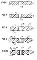
- the substrate S shown in FIG. 1 is a section of a base material for a three-dimensional injection-molded printed circuit board with injected holes LO.
- High-temperature-resistant thermoplastics are particularly suitable as materials for such printed circuit boards, with glass in the exemplary embodiment described fiber-reinforced polyetherimide was used.
- the substrate S shown in FIG. 1 was first pickled to increase the adhesive strength of the conductor tracks and plated-through holes to be applied later and then cleaned.
- Commercial baths were used both for the pickling and for cleaning the substrate S, the pickling bath being specifically matched to the material polyetherimide.
- nucleation B has been applied to the surface of the substrate and the walls of the holes LO.
- the germination B was applied by immersing the substrate S in a PdC [ 2 -SnC [ 2 bath.
- PdC 2 -SnC [ 2 bath.
- Commercial baths based on organic palladium compounds have also proven to be suitable for applying the B seeding.
- the thin base layer G After the thin base layer G has been applied, this is removed again according to FIG. 4 in the regions of the substrate S which do not correspond to the later conductor runs LZ and later plated-through holes DK.
- This selective removal of the base layer G, which corresponds to the generation of a negative conductor pattern, is carried out by ablation using electromagnetic radiation. In this ablation, which will be explained in more detail later with reference to FIG. 15, at the same time, according to FIG. 4, the nucleation B is removed again in the areas that do not correspond to the later conductor lines LZ or later plated-through holes DK.
- GM The metal which is electrodeposited from a commercially available copper bath in the area of the conductor tracks LZ and plated-through holes DK is designated GM in FIG. 5.
- the germination B Before or after activating the germination B, it is then selectively removed again by ablation using electromagnetic radiation. According to FIG. 8, the germination B then only remains in the areas of the later conductor tracks LZ and the later plated-through holes DK.
- a thin layer of chemically deposited metal CM is then applied according to FIG. 9 in the area of the later conductor tracks LZ and the later plated-through holes DK.
- the metal CM is again copper deposited without current.
- the conductor tracks LZ and the plated-through holes DK are galvanically reinforced for the completion of the printed circuit boards, the galvanically deposited metal again being designated GM.
- the substrate S shown in FIG. 11 with holes LO is again assumed, to which, according to FIG. 12, germination B is again applied. Before or after activating the germination B, it is then selectively removed again by ablation using electromagnetic radiation. The remaining germination B in the area of the later conductor tracks LZ and the later plated-through holes DK is shown in FIG. 13.
- the conductor tracks LZ and the plated-through holes DK are then constructed in one go by chemical metal deposition, as shown in FIG.
- the chemically deposited metal layer is again designated CM in FIG. 14.
- This chemically deposited metal CM is a thick copper plating that is electrolessly deposited from a commercially available copper bath.
- FIG. 15 shows a schematic diagram of an arrangement for laser image transmission.
- An Eximer Laser EL can be seen, the laser beam LS of which is directed onto the circuit board LP via a lens LI and an oscillating mirror SS and generates a negative circuit pattern on the circuit board LP.
- a pattem generator can also be arranged downstream of the Eximer Laser EL.
- a lens is then arranged between the pattem generator and the circuit board.
- the image is structured by corresponding displacements and rotations of the circuit board in relation to the pattern generator.
- Such a laser image transmission using a pattern generator can also be used to advantage in the mass production of injection-molded printed circuit boards.
Landscapes
- Chemical & Material Sciences (AREA)
- Engineering & Computer Science (AREA)
- Chemical Kinetics & Catalysis (AREA)
- Metallurgy (AREA)
- Organic Chemistry (AREA)
- Materials Engineering (AREA)
- General Chemical & Material Sciences (AREA)
- Mechanical Engineering (AREA)
- Microelectronics & Electronic Packaging (AREA)
- Manufacturing & Machinery (AREA)
- Health & Medical Sciences (AREA)
- Toxicology (AREA)
- Electrochemistry (AREA)
- Manufacturing Of Printed Wiring (AREA)
- Two-Way Televisions, Distribution Of Moving Picture Or The Like (AREA)
- ing And Chemical Polishing (AREA)
- Chemically Coating (AREA)
Claims (8)
Priority Applications (1)
| Application Number | Priority Date | Filing Date | Title |
|---|---|---|---|
| AT88104882T ATE56050T1 (de) | 1987-04-24 | 1988-03-25 | Verfahren zur herstellung von leiterplatten. |
Applications Claiming Priority (2)
| Application Number | Priority Date | Filing Date | Title |
|---|---|---|---|
| DE3713792 | 1987-04-24 | ||
| DE3713792 | 1987-04-24 |
Publications (2)
| Publication Number | Publication Date |
|---|---|
| EP0287843A1 EP0287843A1 (fr) | 1988-10-26 |
| EP0287843B1 true EP0287843B1 (fr) | 1990-08-29 |
Family
ID=6326243
Family Applications (1)
| Application Number | Title | Priority Date | Filing Date |
|---|---|---|---|
| EP88104882A Expired - Lifetime EP0287843B1 (fr) | 1987-04-24 | 1988-03-25 | Procédé de fabrication de plaques de circuits imprimés |
Country Status (5)
| Country | Link |
|---|---|
| US (1) | US4870751A (fr) |
| EP (1) | EP0287843B1 (fr) |
| JP (1) | JPS63283185A (fr) |
| AT (1) | ATE56050T1 (fr) |
| DE (1) | DE3860511D1 (fr) |
Families Citing this family (35)
| Publication number | Priority date | Publication date | Assignee | Title |
|---|---|---|---|---|
| DE3843230C1 (en) * | 1988-12-22 | 1989-09-21 | W.C. Heraeus Gmbh, 6450 Hanau, De | Process for making a metallic pattern on a base, in particular for the laser structuring of conductor tracks |
| US5013402A (en) * | 1989-01-20 | 1991-05-07 | Casio Computer Co., Ltd. | Method of manufacturing double-sided wiring substrate |
| US4964947A (en) * | 1989-01-20 | 1990-10-23 | Casio Computer Co., Ltd. | Method of manufacturing double-sided wiring substrate |
| WO1991018489A1 (fr) * | 1990-05-16 | 1991-11-28 | Olin Corporation | Procede de fabrication de gtab et produit fabrique de la sorte |
| EP0569417B1 (fr) * | 1991-01-28 | 1995-07-05 | Siemens Aktiengesellschaft | Procede pour fabriquer un support de donnees portable |
| DE59106557D1 (de) * | 1991-11-21 | 1995-10-26 | Siemens Ag | Verfahren zur Herstellung von Leiterplatten. |
| JP3259310B2 (ja) * | 1992-02-25 | 2002-02-25 | 株式会社デンソー | めっき方法及びこのめっき方法により得られる筒状コイル |
| US5310580A (en) * | 1992-04-27 | 1994-05-10 | International Business Machines Corporation | Electroless metal adhesion to organic dielectric material with phase separated morphology |
| IL105925A (en) * | 1992-06-22 | 1997-01-10 | Martin Marietta Corp | Ablative process for printed circuit board technology |
| US5344729A (en) * | 1992-06-26 | 1994-09-06 | Martin Marietta Corporation | Conformal photomask for three-dimensional printed circuit board technology |
| JP2965803B2 (ja) * | 1992-11-19 | 1999-10-18 | ポリプラスチックス株式会社 | 成形品の表面に導電性回路を形成する方法及び導電回路形成部品 |
| JP3153682B2 (ja) * | 1993-08-26 | 2001-04-09 | 松下電工株式会社 | 回路板の製造方法 |
| US5421082A (en) * | 1993-09-22 | 1995-06-06 | Motorola, Inc. | Method of forming a decal having conductive paths thereon |
| BE1007610A3 (nl) * | 1993-10-11 | 1995-08-22 | Philips Electronics Nv | Werkwijze voor het stroomloos aanbrengen van een metaalpatroon op een elektrisch isolerend substraat. |
| US5455741A (en) * | 1993-10-26 | 1995-10-03 | Pulse Engineering, Inc. | Wire-lead through hole interconnect device |
| EP0677985B1 (fr) * | 1994-04-14 | 1999-05-26 | Hewlett-Packard GmbH | Procédé pour la fabrication de panneaux à circuit imprimé |
| DE69426026T2 (de) * | 1994-05-18 | 2001-05-17 | Polyplastics Co. Ltd., Osaka | Verfahren zur herstellung einer leitenden schaltung auf der oberfläche eines formkörpers |
| WO1996015651A1 (fr) * | 1994-11-09 | 1996-05-23 | Blaupunkt-Werke Gmbh | Procede de realisation d'une traversee dans une plaquette a circuit imprime |
| EP0727925A1 (fr) * | 1995-02-14 | 1996-08-21 | Lpkf Cad/Cam Systeme Gmbh | Procédé de métallisation structurée de surfaces de substrats |
| FR2736740A1 (fr) * | 1995-07-11 | 1997-01-17 | Trt Telecom Radio Electr | Procede de production et d'assemblage de carte a circuit integre et carte ainsi obtenue |
| DE19620095B4 (de) * | 1996-05-18 | 2006-07-06 | Tamm, Wilhelm, Dipl.-Ing. (FH) | Verfahren zur Herstellung von Leiterplatten |
| JPH1065315A (ja) * | 1996-08-21 | 1998-03-06 | Totoku Electric Co Ltd | フレキシブルプリント回路の製造方法および該方法により得られたフレキシブルプリント回路 |
| US5878487A (en) * | 1996-09-19 | 1999-03-09 | Ford Motor Company | Method of supporting an electrical circuit on an electrically insulative base substrate |
| US6005463A (en) * | 1997-01-30 | 1999-12-21 | Pulse Engineering | Through-hole interconnect device with isolated wire-leads and component barriers |
| JP3607491B2 (ja) * | 1997-03-04 | 2005-01-05 | 日本特殊陶業株式会社 | 誘電体フィルタの製造方法 |
| JPH11135918A (ja) * | 1997-10-31 | 1999-05-21 | Nippon Avionics Co Ltd | プリント配線板の製造方法 |
| US6131279A (en) | 1998-01-08 | 2000-10-17 | International Business Machines Corporation | Integrated manufacturing packaging process |
| GB2345193B (en) * | 1998-12-22 | 2002-07-24 | Nokia Mobile Phones Ltd | Metallic keys |
| US6349456B1 (en) * | 1998-12-31 | 2002-02-26 | Motorola, Inc. | Method of manufacturing photodefined integral capacitor with self-aligned dielectric and electrodes |
| FR2806935B1 (fr) * | 2000-04-03 | 2002-10-18 | Oreal | Procede pour le decor d'un article, et article decore au moyen du procede |
| US7053011B2 (en) * | 2003-11-04 | 2006-05-30 | Electro Scientific Industries, Inc. | Laser-based termination of passive electronic components |
| WO2006127436A1 (fr) * | 2005-05-20 | 2006-11-30 | Electro Scientific Industries, Inc. | Procede de formation de composants electroniques passifs sur un substrat par des techniques d'ecriture directe utilisant un faisceau laser uniforme forme |
| US7765691B2 (en) * | 2005-12-28 | 2010-08-03 | Intel Corporation | Method and apparatus for a printed circuit board using laser assisted metallization and patterning of a substrate |
| US20140174791A1 (en) * | 2012-12-26 | 2014-06-26 | Unimicron Technology Corp. | Circuit board and manufacturing method thereof |
| US9767957B2 (en) * | 2013-08-12 | 2017-09-19 | Taiwan Semiconductor Manufacturing Co., Ltd. | Method of manufacturing a tunable three dimensional inductor |
Family Cites Families (4)
| Publication number | Priority date | Publication date | Assignee | Title |
|---|---|---|---|---|
| US4085285A (en) * | 1973-11-29 | 1978-04-18 | U.S. Philips Corporation | Method of manufacturing printed circuit boards |
| US4668532A (en) * | 1984-09-04 | 1987-05-26 | Kollmorgen Technologies Corporation | System for selective metallization of electronic interconnection boards |
| JPS61108195A (ja) * | 1984-11-01 | 1986-05-26 | インタ−ナショナル ビジネス マシ−ンズ コ−ポレ−ション | 基板上に電気的に連続した層を形成する方法 |
| US4574095A (en) * | 1984-11-19 | 1986-03-04 | International Business Machines Corporation | Selective deposition of copper |
-
1988
- 1988-03-25 AT AT88104882T patent/ATE56050T1/de not_active IP Right Cessation
- 1988-03-25 EP EP88104882A patent/EP0287843B1/fr not_active Expired - Lifetime
- 1988-03-25 DE DE8888104882T patent/DE3860511D1/de not_active Expired - Lifetime
- 1988-03-31 US US07/176,325 patent/US4870751A/en not_active Expired - Fee Related
- 1988-04-18 JP JP63095372A patent/JPS63283185A/ja active Pending
Also Published As
| Publication number | Publication date |
|---|---|
| JPS63283185A (ja) | 1988-11-21 |
| ATE56050T1 (de) | 1990-09-15 |
| DE3860511D1 (de) | 1990-10-04 |
| EP0287843A1 (fr) | 1988-10-26 |
| US4870751A (en) | 1989-10-03 |
Similar Documents
| Publication | Publication Date | Title |
|---|---|---|
| EP0287843B1 (fr) | Procédé de fabrication de plaques de circuits imprimés | |
| EP0361192B1 (fr) | Procédé de fabrication de plaques de circuit | |
| EP0489759B1 (fr) | Procede pour la fabrication d'une carte de circuits imprimes a trous metallises | |
| EP0109920B1 (fr) | Procédé de nettoyage de trous dans des circuits imprimés avec des solutions de permanganate et des solutions basiques | |
| DE3538652C2 (fr) | ||
| EP1191127B1 (fr) | Procédé pour la métallisation selective de matériaux dielectriques | |
| EP0127689B1 (fr) | Procédé pour la fabrication de circuits imprimés ayant des conducteurs métalliques incrustés dans le support isolant | |
| EP0160966B1 (fr) | Procédé de fabrication d'un dessin métallique sur un substrat isolant et substrat isolant comportant un dessin métallique, en particulier circuits imprimés | |
| EP0060805A1 (fr) | Procédé pour la production de plaquettes imprimées et les plaquettes fabriquées par ce procédé | |
| DE2550598B2 (de) | Verfahren zum Vorbehandeln von Leiterplatten | |
| DE3688255T2 (de) | Verfahren zur herstellung von mehrschichtleiterplatten. | |
| DE69730288T2 (de) | Vorrichtung zur Herstellung von Leiterplatten mit galvanisierten Widerständen | |
| DD296510A5 (de) | Quellmittel zur vorbehandlung von kunstharzen vor einer stromlosen metallisierung | |
| AT392087B (de) | Verfahren zur herstellung von metallisierten kunststoffen sowie zur metallisierung von keramischen materialien | |
| DE69316750T2 (de) | Verfahren zur herstellung einer leiterplatte. | |
| DE3217983A1 (de) | Verfahren und vorrichtung zum herstellen von leiterplatten | |
| EP0417750B1 (fr) | Procédé de metallisation directe de plaques à circuits | |
| EP0757885B1 (fr) | Procede de formation de motifs conducteurs metalliques sur des substrats electriquement isolants | |
| DE3121131C2 (de) | Verfahren zur Herstellung von mit Leiterbahnen versehenen Schaltungsplatten mit metallischen Durchkontaktierungen | |
| EP0543045B1 (fr) | Procédé de fabrication de plaques à circuit imprimé | |
| EP0370133A1 (fr) | Procédé de fabrication d'un circuit imprimé | |
| DE3931003A1 (de) | Verfahren zur direkten metallisierung von leiterplatten | |
| EP0581823B1 (fr) | Agent pour la formation selective d'une couche mince oxydante | |
| EP0530564A1 (fr) | Procédé pour la fabrication d'un panneau de circuit | |
| DE3048665C2 (fr) |
Legal Events
| Date | Code | Title | Description |
|---|---|---|---|
| PUAI | Public reference made under article 153(3) epc to a published international application that has entered the european phase |
Free format text: ORIGINAL CODE: 0009012 |
|
| AK | Designated contracting states |
Kind code of ref document: A1 Designated state(s): AT BE CH DE FR GB IT LI NL |
|
| 17P | Request for examination filed |
Effective date: 19881125 |
|
| 17Q | First examination report despatched |
Effective date: 19900201 |
|
| GRAA | (expected) grant |
Free format text: ORIGINAL CODE: 0009210 |
|
| AK | Designated contracting states |
Kind code of ref document: B1 Designated state(s): AT BE CH DE FR GB IT LI NL |
|
| PG25 | Lapsed in a contracting state [announced via postgrant information from national office to epo] |
Ref country code: IT Free format text: LAPSE BECAUSE OF FAILURE TO SUBMIT A TRANSLATION OF THE DESCRIPTION OR TO PAY THE FEE WITHIN THE PRESCRIBED TIME-LIMIT;WARNING: LAPSES OF ITALIAN PATENTS WITH EFFECTIVE DATE BEFORE 2007 MAY HAVE OCCURRED AT ANY TIME BEFORE 2007. THE CORRECT EFFECTIVE DATE MAY BE DIFFERENT FROM THE ONE RECORDED. Effective date: 19900829 |
|
| REF | Corresponds to: |
Ref document number: 56050 Country of ref document: AT Date of ref document: 19900915 Kind code of ref document: T |
|
| REF | Corresponds to: |
Ref document number: 3860511 Country of ref document: DE Date of ref document: 19901004 |
|
| ET | Fr: translation filed | ||
| GBT | Gb: translation of ep patent filed (gb section 77(6)(a)/1977) | ||
| PLBE | No opposition filed within time limit |
Free format text: ORIGINAL CODE: 0009261 |
|
| STAA | Information on the status of an ep patent application or granted ep patent |
Free format text: STATUS: NO OPPOSITION FILED WITHIN TIME LIMIT |
|
| 26N | No opposition filed | ||
| ITTA | It: last paid annual fee | ||
| PGFP | Annual fee paid to national office [announced via postgrant information from national office to epo] |
Ref country code: DE Payment date: 19920521 Year of fee payment: 5 |
|
| PGFP | Annual fee paid to national office [announced via postgrant information from national office to epo] |
Ref country code: CH Payment date: 19920622 Year of fee payment: 5 |
|
| PGFP | Annual fee paid to national office [announced via postgrant information from national office to epo] |
Ref country code: GB Payment date: 19930216 Year of fee payment: 6 |
|
| PGFP | Annual fee paid to national office [announced via postgrant information from national office to epo] |
Ref country code: AT Payment date: 19930224 Year of fee payment: 6 |
|
| PGFP | Annual fee paid to national office [announced via postgrant information from national office to epo] |
Ref country code: BE Payment date: 19930312 Year of fee payment: 6 |
|
| PGFP | Annual fee paid to national office [announced via postgrant information from national office to epo] |
Ref country code: FR Payment date: 19930319 Year of fee payment: 6 |
|
| PG25 | Lapsed in a contracting state [announced via postgrant information from national office to epo] |
Ref country code: LI Effective date: 19930331 Ref country code: CH Effective date: 19930331 |
|
| PGFP | Annual fee paid to national office [announced via postgrant information from national office to epo] |
Ref country code: NL Payment date: 19930331 Year of fee payment: 6 |
|
| REG | Reference to a national code |
Ref country code: CH Ref legal event code: PL |
|
| PG25 | Lapsed in a contracting state [announced via postgrant information from national office to epo] |
Ref country code: DE Effective date: 19931201 |
|
| PG25 | Lapsed in a contracting state [announced via postgrant information from national office to epo] |
Ref country code: GB Effective date: 19940325 Ref country code: AT Effective date: 19940325 |
|
| PG25 | Lapsed in a contracting state [announced via postgrant information from national office to epo] |
Ref country code: BE Effective date: 19940331 |
|
| BERE | Be: lapsed |
Owner name: SIEMENS A.G. Effective date: 19940331 |
|
| PG25 | Lapsed in a contracting state [announced via postgrant information from national office to epo] |
Ref country code: NL Effective date: 19941001 |
|
| NLV4 | Nl: lapsed or anulled due to non-payment of the annual fee | ||
| GBPC | Gb: european patent ceased through non-payment of renewal fee |
Effective date: 19940325 |
|
| PG25 | Lapsed in a contracting state [announced via postgrant information from national office to epo] |
Ref country code: FR Effective date: 19941130 |
|
| REG | Reference to a national code |
Ref country code: FR Ref legal event code: ST |