EP0288001A2 - Verfahren zur Herstellung einer supraleitenden dünnen Schicht und Anordnung zu seiner Durchführung - Google Patents
Verfahren zur Herstellung einer supraleitenden dünnen Schicht und Anordnung zu seiner Durchführung Download PDFInfo
- Publication number
- EP0288001A2 EP0288001A2 EP88106211A EP88106211A EP0288001A2 EP 0288001 A2 EP0288001 A2 EP 0288001A2 EP 88106211 A EP88106211 A EP 88106211A EP 88106211 A EP88106211 A EP 88106211A EP 0288001 A2 EP0288001 A2 EP 0288001A2
- Authority
- EP
- European Patent Office
- Prior art keywords
- oxide
- substrate
- metal
- copper
- oxygen
- Prior art date
- Legal status (The legal status is an assumption and is not a legal conclusion. Google has not performed a legal analysis and makes no representation as to the accuracy of the status listed.)
- Granted
Links
Images

Classifications
-
- H—ELECTRICITY
- H10—SEMICONDUCTOR DEVICES; ELECTRIC SOLID-STATE DEVICES NOT OTHERWISE PROVIDED FOR
- H10N—ELECTRIC SOLID-STATE DEVICES NOT OTHERWISE PROVIDED FOR
- H10N60/00—Superconducting devices
- H10N60/01—Manufacture or treatment
- H10N60/0268—Manufacture or treatment of devices comprising copper oxide
- H10N60/0296—Processes for depositing or forming copper oxide superconductor layers
- H10N60/0548—Processes for depositing or forming copper oxide superconductor layers by deposition and subsequent treatment, e.g. oxidation of pre-deposited material
-
- H—ELECTRICITY
- H10—SEMICONDUCTOR DEVICES; ELECTRIC SOLID-STATE DEVICES NOT OTHERWISE PROVIDED FOR
- H10N—ELECTRIC SOLID-STATE DEVICES NOT OTHERWISE PROVIDED FOR
- H10N60/00—Superconducting devices
- H10N60/01—Manufacture or treatment
- H10N60/0268—Manufacture or treatment of devices comprising copper oxide
- H10N60/0296—Processes for depositing or forming copper oxide superconductor layers
- H10N60/0408—Processes for depositing or forming copper oxide superconductor layers by sputtering
Definitions
- the present invention relates to a process for producing a superconducting thin film, notably a process for forming a superconducting thin film made of IIa-IIIa-Cu oxide on the surface of a substrate.
- Superconducting materials hold much promise for use in varous cryoelectronic devices such as Josephson devices and SQUID (superconducting quantum interference device) sensors.
- various oxide ceramics have conventionally been prepared by the sintering process. The oxide ceramics so far proposed are described below together with the transition temperatures at which they start to manifest superconductivity:
- Superconducting materials need to be processed into thin films in order that they can be used in cryoelectronic devices such as Josephson devices and SQUID sensors.
- cryoelectronic devices such as Josephson devices and SQUID sensors.
- conventional superconducting materials have been processed into oxide ceramics by the sintering process, which is practically ineffective for the production of superconducting thin films.
- An object, therefore, of the present invention is to provide a process for forming a superconducting thin film on the surface of a substrate.
- This object of the present invention can be attained by forming a superconducting thin film of IIa-IIIa-Cu oxide which comprises depositing on the surface of a substrate the vapors of a group IIa metal and/or an oxide thereof, a group IIIa metal and/or an oxide thereof, and copper and/or an oxide thereof while the substrate is irradiated with an oxygen neutral beam during deposition of such vapors.
- the evaporated metals or oxides thereof will descend slowly to be deposited on the substrate.
- the substrate is irradiated with an oxygen neutral beam which effectively implants these metals or oxides thereof into the substrate, forming a mixing layer at the interface between the substrate and the overlying metal or metal oxide layer.
- This mixing layer renders deposited coatings to be strongly adherent to the substrate so that they will not readily separate from the latter.
- the evaporated metal will be oxidized with the oxygen neutral beam as it is deposited on the substrate, and the evaporated metal oxide will be supplied with oxygen in an amount compensating for the loss that occurred during vapor deposition. As a result of these procedures, a superconducting thin film made of a IIa-IIIa-Cu oxide is formed on the substrate.
- a group IIa metal and/or an oxide thereof, a group IIIa metal and/or an oxide thereof, and copper and/or an oxide thereof are evaporated simultaneously to form a film made of the IIa-IIIa-Cu oxide, i.e., the oxide of the mixture of the IIa, IIIa and Cu.
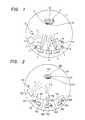
- Fig. 1 is a schematic diagram illustrating a thin-film forming apparatus that may be employed in implementing a process according to the first embodiment of the present invention.
- This apparatus of Fig. 1 forms a thin film by the ion vapor deposition (IVD) process and comprises a vacuum chamber 1 which contains three crucibles 2, 3 and 4 charged with respective metals serving as evaporation sources, an oxygen ion source 5, and a substrate holder 6.
- IVD ion vapor deposition
- the crucibles 2, 3 and 4 are respectively charged with a group IIa metal (e.g. Sr or Ba) or an oxide thereof, a group IIIa metal (e.g. Sc, Y or La) or an oxide thereof, and copper or an oxide thereof.
- the crucibles 2, 3 and 4 are respectively irradiated with electron beams a, b and c supplied from electron beam sources 7, 8 and 9 and the metals or oxides thereof in the respective crucibles are evaporated as indicated by d, e and f.
- the oxygen ion source 5 generates an oxygen ion beam in the interior of the vacuum chamber 1.
- a neutralizer 10 is positioned close to the oxygen ion source 5, and the oxygen ions generated from said source are neutralized to an oxygen neutral beam h. Since the thin film 13 is formed on the substrate 11 on the substrate holder 6 is an insulator, static charges will build up on the surface of this thin film 13 as a result of irraidation of the pure oxygen ions and if the static buildup exceeds a certain limit, ensuing oxygen ion beams will be repelled or insulation breakdown of the film will occur. Neutralization of the ion beam generated from the oxygen ion source 5 is effective in preventing such troubles.
- the neutralizer 10 may be in the form of a neutralizing filament made of a suitable metal such as tantalum or tungsten.
- the electrons generated from this filament will neutralize the oxygen ions.
- the oxygen neutral beam h is preferably radiated in a quantity slightly greater than what is necessary to oxidize evaporated metals.
- the substrate holder 6 has a built-in heater 12 and is fitted on its surface with the substrate 11 made of an insulating material such as sapphire or zirconia.
- the metals or oxides thereof in the crucibles 2, 3 and 4 are evaporated by the action of electron beams a, b and c generated from the electron beam sources 7, 8 and 9, respectively, and are deposited on the substrate 11 attached to the surface of the substrate holder 6.
- the proportions of the metals or oxides thereof to be deposited can be appropriately determined by controlling the doses of electron beams and hence the temperatures to which the filaments in the respective electron beam sources are heated.
- the temperatures of the respective filaments are set at such values that the total amount of a group IIa metal and/or an oxide thereof and a group IIIa metal and/or an oxide thereof will be approximately equal to the amount of copper or an oxide thereof as measured on the surface of the substrate 11.
- the oxygen ions generated from the oxygen ion source and which have been neutralized with the neutralizer 10 into an oxygen neutral beam h are directed onto the surface of the substrate 11.
- the oxygen neutral beam h not only implants the evaporated metals or oxides thereof into the substrate 11 but also reacts with them to form a superconducting thin film 13 of a IIa-IIIa-Cu oxide on the surface of the substrate 11.
- the process of the present invention may also be employed to form a coating of a superconducting thin film of IIa-IIIa-Cu oxide on the substrate 11 in wire form.
- the resulting product can be used as a superconducting coil.
- the substrate 11 is heated with the built-in heater 12 during evaporation.
- the respective metals or oxides thereof may be evaporated with the substrate 11 being unheated or heated at about 200°C, and with the evaporated metals or oxides thereof being subsequently annealed to become crystalline.
- the three metals or oxides thereof to be deposited are evaporated individually and this has the advantage of enabling the proportions of these metals or oxides thereof to be easily controlled.
- an alloy of the three metals or an oxide thereof may be used as an evaporant.
- a mixture or an alloy of a group IIa metal and/or an oxide thereof and a group IIIa metal and/or an oxide thereof may be charged into one of the two crucibles, with copper and/or an oxide thereof being charged into the other crucible.
- the substrate was made of a sapphire crystal (C-face cleaved) which was heated at 800°C during evaporation.
- An oxygen ion beam was used as an oxygen ion source.
- a beam having an energy of 100 eV and 1 mA/cm2 (on the substrate) was neutralized with a neutralizer and the resulting oxygen neutral beam was directed onto the substrate.
- the above-described first embodiment of the present invention has the advantage that it enables the formation of a superconducting thin film made of IIa-IIIa-Cu oxide.
- a group IIa metal and/or an oxide thereof, a group IIIa metal and/or an oxide thereof, and copper and/or an oxide thereof are evaporated successively, or alternatively, the evaporation of copper and/or an oxide thereof alternates with the evaporation of the two other metals and/or oxides thereof.
- the substrate is irradiated with an oxygen neutral beam so as to form a superconducting thin film made of laminated IIa, IIIa and Cu oxide layers.
- the evaporated metals or oxides thereof descent slowly to be deposited in superposition on the substrate.
- the substrate is irradiated with an oxygen neutral beam which effectively implants metals or metal oxides into the substrate or into layers that have already been deposited on the substrate, thereby forming a mixing layer at the interface between the substrate and overlying metal or metal oxide layers or between adjacent metal or metal oxide layers.
- This mixing layer renders deposited coatings to be strongly adherent to one another or to the substrate so that they will not readily separate from one another or from the substrate.
- the evaporated metal will be oxidized with the oxygen neutral beam as it is deposited on the substrate, and the evaporated metal oxide will be supplied with oxygen in an amount that compensates for the loss that occurred during vapor deposition.
- a superconducting thin film is formed that consists of IIa, IIIa and Cu oxide layers in superposition on the substrate. This thin film will easily make the transition to the superconducting state by virtue of the homogeneity of its crystalline structure.
- Fig. 2 is a schematic diagram illustrating a thin-film forming apparatus that may be employed in implementing a process according to the second embodiment of the present invention.
- This apparatus forms a thin film by the ion vapor deposition (IVD) process and comprises a vacuum chamber 101 which contains three crucibles 102, 103 and 104 charged with respective metals serving as evaporation sources, an oxygen ion source 105, and a substrate holder 106.
- IVD ion vapor deposition
- the crucibles 102, 103 and 104 are respectively charged with a group IIa metal (e.g. Sr or Ba) and/or an oxide thereof, a group IIIa metal (e.g. Sc, Y or La) and/or an oxide thereof, and copper and/or an oxide thereof.
- the crucibles 102, 103 and 104 are respectively irradiated with electron beams a, b and c supplied from electron beam sources 107, 108 and 109 and the metals or oxides thereof in the respective crucibles are evaporated.
- the crucibles 102, 103 and 104 making pairs with the associated electron beam sources 107, 108 and 109 are accommodated within evaporation compartments 114, 115 and 116 which are respectively equipped with shutters 117, 118 and 119 that can be slid to be opened or closed.
- the oxygen ion source 105 generates oxygen ions in the interior of the vacuum chamber 101.
- a neutralizer 110 is positioned close to the oxygen ion source 105, and the generated oxygen ions are neutralized to an oxygen neutral beam h. If oxygen ions are directly allowed to impinge on the substrate 111 on the substrate holder 106, static charges will build up on the surface of the thin film being formed on the substrate. If the static buildup exceeds a certain limit, ensuing oxygen ions will be repelled or insulation breakdown of the film will occur. Neutralization of the ions generated from the oxygen ion source 105 is effective in preventing such troubles.
- the neutralizer 110 may be in the form of a neutralizing filament made of a suitable metal such as tantalum or tungsten. The electrons generated from this filament will neutralize the oxygen ions.
- the oxygen neutral beam h is preferably radiated in a quantity slightly greater than what is necessary to oxidize evaporated metals.
- the substrate holder 106 has a built-in heater 112 and is fitted on its surface with the substrate 111 made of an insulating material such as sapphire or zirconia.
- the metals or oxides thereof in the crucibles 102, 103 and 104 are evaporated by the action of electron beams a, b and c generated from the electron beam sources 107, 108 and 109, respectively.
- This evaporation is performed with either one of the shutters 117, 118 and 119 being opened while the others remain closed. If this selective opening of shutters is effected cylically at given time intervals, layers of predetermined amounts of the evaporated metals or oxides thereof can be deposited in superposition on the surface of the substrate 111. In the case shown in Fig. 2, only the shutter 118 on the evaporation compartment 115 is opened and the heated metal or oxide thereof is evaporated as indicated by d.
- the amounts in which the metals or oxides thereof evaporated from the compartments 114 through 116 are deposited on the substrate can be appropriately determined by controlling the doses of electron beams and hence the temperatures to which the filaments in the respective electron beam sources are heated, as well as the time period during which shutters 117 through 119 are selectively opened.
- the respective layers are deposited in superposition in such a way that the total amount of a group IIa metal and/or an oxide thereof and a group IIIa metal and/or an oxide thereof will be approximately equal to the amount of copper and/or an oxide thereof as measured on the surface of the substrate 111.
- the order in which the layers are deposited in superposition is determined by the order in which the shutters 117 through 119 are selectively opened.
- the oxygen ion beam generated from the oxygen ion source and which has been neutralized with the neutralizer 110 into an oxygen neutral beam h is directed onto the surface of the substrate 111.
- This oxygen neutral beam h not only oxidizes the metals in the process of successive deposition to form oxides but also implants the evaporated metals or oxides thereof into the substrate 111 and into deposited coatings on the substrate, thereby forming mixing layers at the interface between the substrate and overlying layers and between adjacent layers.
- a superconducting thin film 113 is formed in which the layers of oxides of a group IIa metal, a group IIIa metal and copper are deposited in superposition, with the individual layer adhering strongly to one another.
- the process of the present invention may also be employed to form a coating of a superconducting thin film composed of IIa, IIIa and Cu oxides in layers on the substrate 111 in wire form.
- the resulting product can be used as a superconducting coil.
- the substrate 111 is heated at about 800°C with the built-in heater 112 during evaporation.
- the respective metals or oxides thereof may be evaporated with the substrate 111 being unheated or heated at about 200°C, and with the evaporated metals or oxides thereof being subsequently annealed to become crystalline.
- the three metals or oxides thereof to be deposited are evaporated successively from compartments 114, 115 and 116 and this has the advantage of enabling the proportions of these metals or oxides thereof to be easily controlled. If de-sired, the shutter on the compartment where a group IIa metal and/or an oxide thereof is to be evaporated and the shutter on the compartment where a group IIIa metal and/or an oxide thereof is to be evaporated may be opened simul-taneously so that a mixed oxide of the two metal is vapor-deposited alternately with a copper oxide layer. This approach would cause no problem since superconductivity is considered to take place chiefly in the copper oxide layer.
- two evaporation compartments are provided and a group IIa metal and/or an oxide thereof are accommodated in one compartment whereas copper and/or an oxide thereof is charged into the other compartment, with the shutters on the two compartments being allowed to open in turns.
- the group IIa metal and/or an oxide thereof and the group IIIa metal and/or an oxide thereof may be accommodated in one compartment either on their own or as an admixture. If desired, an alloy of these metals or an oxide thereof may be used as an evaporant. All of the modifications described above are included within the scope of the present invention.
- Three evaporation compartments were charged with Y, Ba and Cu, respectively, which were evaporated at the rates noted below, with the shutters on the three compartments being opened for 3 seconds and then closed in the following manner: Cu evaporation compartment open; Cu evaporation compartment closed; Y and Ba evaporation compartments open; Y and Ba evaporation compartments closed; Cu evaporation compartment open; Cu evaporation compartment closed; Y and Ba evaporation compartments open; and ⁇ .
- an oxygen neutral beam was directed onto the substrate.
- the oxygen neutral beam was produced by neutralizing with a neutralizer an oxygen ion beam having an energy of 100 eV and 0.7 mA/cm2 (on the substrate).
- the substrate used was made of a sapphire crystal (C face cleaved) which was heated at 800°C during deposition of layers in superposition.
- a superconducing thin film with a total thickness of 5,000 ⁇ and which was made of Y, Ba and Cu oxides in layers was formed on the surface of the sapphire substrate.
- a gold electrode was formed on both sides of this superconducting thin film by sputtering and the electrical resistance across this film was measured in liquid nitro-gen. Zero resistance was observed between the electrodes.
- the above-described second embodiment of the present invention has the advantage that it enables the formation of a superconducting thin film consisting of superposed layers of IIa, IIIa and Cu oxides.
- a group IIa metal and/or an oxide thereof, a group IIIa metal and/or an oxide thereof and copper and/or an oxide thereof may be deposited in superposition on a substrate by sputtering rather than evaporation.
- a group IIa metal and/or an oxide thereof, a group III metal and/or an oxide thereof and copper and/or an oxide thereof are sputtered successively, or alternatively, the sputtering of copper and/or an oxide thereof alternates with the puttering of the two other metals and/or oxides thereof.
- the substrate is irradiated with an oxygen neutral beam so as to form a superconducting thin film made of laminated IIa, IIIa and Cu oxide layers.
- the sputtered metals or oxides thereof are deposited in superposition on the substrate, forming a multilayered structure (artificial lattice).
- the oxygen neutral beam being directed to impinge on the substrate oxidizes sputtered metals into their oxide form, whereas it supplies sputtered metal oxides with oxygen in an amount sufficient to compensate for the loss that occurred during sputtering.
- the oxygen neutral beam also serves as an effective means to implant metals or metal oxides into the substrate or into layers that have already been deposited on the substrate, thereby forming a mixing layer at the interface between the substrate and overlying metal or metal oxide layers or between adjacent metal or metal oxide layers.
- This mixing layer renders deposited coatings to be strongly adherent to one another or to the substrate so that they will not readily separate from one another or from the substrate.
- a superconducting thin film is formed that consists of IIa, IIIa and Cu oxide layers in superposition (i.e., multilayered structure) on the substrate. This thin film will readily make the transition to the superconducting state by virtue of the homigeneity of its crystalline structure.
- FIG. 3 is a schematic diagram illustrating a thin-film forming apparatus that may be employed in implementing a process according to the third embodiment of the present invention.
- This apparatus forms a thin film by ion beam sputtering and comprises a vacuum chamber 201 which contains three compartments 202, 203 and 204 for generating sputtered particles, an oxygen ion source 205, and a substrate holder 206.
- the compartments 202, 203 and 204 respectively contain sputtering ion sources 207, 208 and 209, as well as associated targets 210, 211 and 212.
- Each of the ion sources 207, 208 and 209 is so designed that an inert gas such as argon is ionized and extracted through an extracting electrode system.
- Neutralizers 213, 214 and 215 are disposed in the vicinity of the ion sources 207, 208 and 209, respectively, and the Ar ion beams produced from the ion sources are neutralized with these neutralizers to form Ar neutral beams a ⁇ , b ⁇ and c ⁇ , which will sputter the respective targets 210, 211 and 212.
- Each of the neutralizers 213, 214 and 215 is in the form of a neutralizing filament made of a suitable metal such as tungsten or tantalum. If the targets 210 through 212 are made of an insulating material, static charges will build up as a result of impingement of an ion beam and if they exceed a certain limit, insulation breakdown occurs and the targets will be disrupted. Neutralization of the Ar ion beams is effective in preventing such troubles and is not particularly needed if the targets are made of a metal.
- the targets 210 through 212 are respectively made of a group IIa metal and/or an oxide thereof, a group IIIa metal and/or an oxide thereof, and copper and/or an oxide thereof, and they are prepared by calcining the powders of these materials at an elevated temperature in the range of from about 1,000 to about 1,200°C.
- the compartments 202, 203 and 204 are respectively equipped with shutters 217, 218 and 219 that can be slid to be opened or closed.
- the order in which these shutters are selectively opened determines the order in which layers are deposited, and the period of time during which they are opened determines the thickness of individual layers to be deposited.
- the oxygen ion source 205 generates an oxygen ion beam in the interior of the vacuum chamber 201.
- a neutralizer 220 is positioned close to the oxygen ion source 205, and the generated oxygen ion beam is neutralized to an oxygen neutral beam h. If oxygen ions are directly allowed to impinge on the substrate 222 on the substrate holder 206, static charges will build up on the surface of the thin film being formed on the substrate. If the static buildup exceeds a certain limit, ensuing oxygen ions will be repelled or insulation breakdown of the film will occur. Neutralization of the oxygen ions generated from the oxygen source 205 is effective in preventing such troubles.
- the neutralizer 220 may be in the form of a neutralizing filament made of a suitable metal such as tantalum or tungsten.
- the electrons generated from this filament will neutralize the oxygen ions.
- the oxygen neutral beam h is preferably radiated in a quantity slightly greater than what is necessary to oxidize deposited metals.
- the substrate holder 206 has a built-in heater 221 and is fitted on its surface with the substrate 222 made of an insulating material such as sapphire or zirconia.
- Ion beams with an energy of the order of 500 through 2,000 eV that have been extracted from the sputtering ion sources 207 through 209 are neutralized with the neutralizers 210, 211 and 212 into neutral beams.
- the neutral beams sputter the targets 210 through 212 from which sputtered particles will be emitted.
- This sputtering operation is performed with either one of the shutters 217, 218 and 219 being opened while the others remain closed. If this selective opening of shutters is effected cyclically at given intervals, layers of predetermined amounts of the sputtered particles of the respective metals or oxides thereof can be deposited in superposition on the surface of the substrate 222. In the case shown in Fig.
- a superconducting thin film 213 is formed in which the layers of oxides of a group IIa metal, a group IIIa metal and copper are deposited in superposition, with the individual layers ad-hering strongly to one another.
- the process of the embodiment may also be employed to form a coating of a superconducting thin film composed of IIa, IIIa and Cu oxides in layers on the substrate 222 in wire form. The resulting product can be used as a superconducting coil.
- the substrate 222 In order to accelerate the reaction taking place on the substrate 222, the latter is heated at about 700°C with the built-in heater 221 during sputtering. Alternatively, the respective metals or oxides thereof may be sputtered with the substrate 222 being unheated or heated at about 200°C, and with the sputtered metals or oxides thereof being subsequently annealed.
- the three metals or oxides thereof in the compartments 202, 203 and 204 are successively sputtered to knock off particles therefrom, and this has the advantage of enabling the proportions of these metals or oxides thereof to be easily controlled.
- the shutter on the compartment accommodating a group IIa metal and/or an oxide thereof and the shutter on the compartment containing a group IIIa metal and/or an oxide thereof may be opened simultaneously so that a mixed oxide of the two metals is deposited alternately with a copper oxide layer.
- two evaporation compartments are provided and a group IIa metal and/or an oxide thereof and a group IIIa metal and/or an oxide thereof are accommodated as a mixed target in one compartment, whereas copper and/or an oxide thereof is charged as a target into the other compartment, with the shutters on the two compartments being allowed to open in turns.
- the group IIa metal and/or an oxide thereof and the group IIIa metal and/or an oxide thereof may be accommodated as separate targets in the one compartment. If desired, an alloy of these metals or an oxide thereof may be used as a target. All of the modifications described above are included within the cope of the present invention.
- a sapphire substrate 222 was heated at 200°C.
- An Ar ion beam was used as a sputtering ion source and controlled to have an energy of 1 keV and 1 mA.
- An oxygen ion beam was used as an oxygen ion source and controlled to have an energy of 100 V and 0.5 mA. This oxygen ion beam was neutralized and bombarded against the substrate.
- a multi-layered film was produced by cyclically opening and closing the shutters on the three compartments in the following way: Cu compartment open; Cu compartment closed; Ba compartment open, Ba compartment closed; Cu compartment open; Cu compartment closed; Y compartment open; Y compartment closed; Cu compartment open; and ⁇ .
- the duration of time for which each shutter was allowed to open was controlled so that each of the layers of Y, Ba and Cu oxides would be deposited in a thickness of 5 ⁇ .
- the deposited layers were annealed at 700°C in an electric furnace.
- a superconducting thin film with a total thickness of 1,000 ⁇ and which was made of Y, Ba and Cu oxides in superposed layers was formed on the surface of the sapphire substrate.
- a gold electrode was formed on both sides of this superconducting thin film by sputtering and the electrical resistance across this film was measured in liquid nitrogen. Zero resistance was observed between the electrodes.
- the above-described third embodiment of the present invention has the advantage that it enables the formation of a superconducting thin film consisting of superposed layers of IIa, IIIa and Cu oxides.
- the film may have either the construction that the film consists of layers of IIa, IIIa and Cu oxides superposed on one another or the construction that the film is made of IIa-IIIa-Cu oxide
Landscapes
- Engineering & Computer Science (AREA)
- Manufacturing & Machinery (AREA)
- Superconductors And Manufacturing Methods Therefor (AREA)
- Inorganic Compounds Of Heavy Metals (AREA)
- Physical Vapour Deposition (AREA)
- Superconductor Devices And Manufacturing Methods Thereof (AREA)
Applications Claiming Priority (6)
| Application Number | Priority Date | Filing Date | Title |
|---|---|---|---|
| JP96787/87 | 1987-04-20 | ||
| JP62096785A JP2521950B2 (ja) | 1987-04-20 | 1987-04-20 | 超電導薄膜の製造方法 |
| JP62096786A JPS63261627A (ja) | 1987-04-20 | 1987-04-20 | 超電導薄膜の製造方法 |
| JP62096787A JPS63261628A (ja) | 1987-04-20 | 1987-04-20 | 超電導薄膜の製造方法 |
| JP96785/87 | 1987-04-20 | ||
| JP96786/87 | 1987-04-20 |
Publications (3)
| Publication Number | Publication Date |
|---|---|
| EP0288001A2 true EP0288001A2 (de) | 1988-10-26 |
| EP0288001A3 EP0288001A3 (en) | 1989-10-18 |
| EP0288001B1 EP0288001B1 (de) | 1993-01-13 |
Family
ID=27308213
Family Applications (1)
| Application Number | Title | Priority Date | Filing Date |
|---|---|---|---|
| EP88106211A Expired - Lifetime EP0288001B1 (de) | 1987-04-20 | 1988-04-19 | Verfahren zur Herstellung einer supraleitenden dünnen Schicht und Anordnung zu seiner Durchführung |
Country Status (3)
| Country | Link |
|---|---|
| US (1) | US4861750A (de) |
| EP (1) | EP0288001B1 (de) |
| DE (1) | DE3877405T2 (de) |
Cited By (2)
| Publication number | Priority date | Publication date | Assignee | Title |
|---|---|---|---|---|
| DE3815185A1 (de) * | 1987-08-05 | 1989-02-16 | Siemens Ag | Verfahren zur herstellung einer hybridstruktur mit halbleitendem und supraleitendem material |
| EP0292958A3 (en) * | 1987-05-26 | 1989-10-11 | Sumitomo Electric Industries, Limited | Method for preparing thin film of compound oxide superconductor |
Families Citing this family (15)
| Publication number | Priority date | Publication date | Assignee | Title |
|---|---|---|---|---|
| US4888202A (en) * | 1986-07-31 | 1989-12-19 | Nippon Telegraph And Telephone Corporation | Method of manufacturing thin compound oxide film and apparatus for manufacturing thin oxide film |
| CA1332324C (en) * | 1987-03-30 | 1994-10-11 | Jun Shioya | Method for producing thin film of oxide superconductor |
| JPH075435B2 (ja) * | 1987-03-31 | 1995-01-25 | 住友電気工業株式会社 | 超電導薄膜の製造方法及び装置 |
| US5158931A (en) * | 1988-03-16 | 1992-10-27 | Kabushiki Kaisha Toshiba | Method for manufacturing an oxide superconductor thin film |
| JPH031584A (ja) * | 1989-02-04 | 1991-01-08 | Riken Corp | ジョセフソン接合素子の製造方法 |
| JPH02310363A (ja) * | 1989-05-24 | 1990-12-26 | Mitsubishi Electric Corp | レーザ蒸着装置 |
| JPH03111578A (ja) * | 1989-06-29 | 1991-05-13 | Toshiba Corp | 薄膜形成方法及び薄膜形成装置 |
| JP2767298B2 (ja) * | 1989-09-05 | 1998-06-18 | 財団法人生産開発科学研究所 | 積層薄膜体及びその製造法 |
| US5264413A (en) * | 1990-03-07 | 1993-11-23 | Ivan Bozovic | Bi-Sr-Ca-Cu-O compounds and methods |
| WO2001026143A1 (en) | 1999-10-04 | 2001-04-12 | Matsushita Eletric Industrial Co., Ltd. | Method of manufacturing semiconductor device |
| US6756320B2 (en) * | 2002-01-18 | 2004-06-29 | Freescale Semiconductor, Inc. | Method of forming article comprising an oxide layer on a GaAs-based semiconductor structure |
| US7442654B2 (en) | 2002-01-18 | 2008-10-28 | Freescale Semiconductor, Inc. | Method of forming an oxide layer on a compound semiconductor structure |
| US8261690B2 (en) * | 2006-07-14 | 2012-09-11 | Georgia Tech Research Corporation | In-situ flux measurement devices, methods, and systems |
| US7846807B2 (en) * | 2008-06-19 | 2010-12-07 | Hermes-Epitek Corp. | Method for forming memristor material and electrode structure with memristance |
| US9023422B1 (en) * | 2011-08-31 | 2015-05-05 | Maxim Integrated Products, Inc. | High rate deposition method of magnetic nanocomposites |
Family Cites Families (4)
| Publication number | Priority date | Publication date | Assignee | Title |
|---|---|---|---|---|
| JPS6115967A (ja) * | 1984-06-29 | 1986-01-24 | Sumitomo Electric Ind Ltd | 表面処理方法 |
| JPS6124214A (ja) * | 1984-07-12 | 1986-02-01 | Taiyo Yuden Co Ltd | Co−O系薄膜型垂直磁気記録媒体の製造方法 |
| CA1332324C (en) * | 1987-03-30 | 1994-10-11 | Jun Shioya | Method for producing thin film of oxide superconductor |
| JPH075435B2 (ja) * | 1987-03-31 | 1995-01-25 | 住友電気工業株式会社 | 超電導薄膜の製造方法及び装置 |
-
1988
- 1988-04-19 DE DE8888106211T patent/DE3877405T2/de not_active Expired - Fee Related
- 1988-04-19 EP EP88106211A patent/EP0288001B1/de not_active Expired - Lifetime
- 1988-04-19 US US07/183,099 patent/US4861750A/en not_active Expired - Fee Related
Cited By (3)
| Publication number | Priority date | Publication date | Assignee | Title |
|---|---|---|---|---|
| EP0292958A3 (en) * | 1987-05-26 | 1989-10-11 | Sumitomo Electric Industries, Limited | Method for preparing thin film of compound oxide superconductor |
| US4925829A (en) * | 1987-05-26 | 1990-05-15 | Sumitomo Electric Industries, Ltd. | Method for preparing thin film of compound oxide superconductor by ion beam techniques |
| DE3815185A1 (de) * | 1987-08-05 | 1989-02-16 | Siemens Ag | Verfahren zur herstellung einer hybridstruktur mit halbleitendem und supraleitendem material |
Also Published As
| Publication number | Publication date |
|---|---|
| US4861750A (en) | 1989-08-29 |
| DE3877405D1 (de) | 1993-02-25 |
| EP0288001A3 (en) | 1989-10-18 |
| DE3877405T2 (de) | 1993-05-06 |
| EP0288001B1 (de) | 1993-01-13 |
Similar Documents
| Publication | Publication Date | Title |
|---|---|---|
| EP0288001B1 (de) | Verfahren zur Herstellung einer supraleitenden dünnen Schicht und Anordnung zu seiner Durchführung | |
| US4920094A (en) | Process for producing superconducting thin films | |
| EP0302506B1 (de) | Verfahren und Vorrichtung zur Herstellung supraleitender Dünnschichten | |
| US4874741A (en) | Non-enhanced laser evaporation of oxide superconductors | |
| EP0269112A2 (de) | Verfahren zum Herstellen eines dünnen kristallischen Films | |
| JP2588985B2 (ja) | 酸化物薄膜の成膜方法 | |
| JPS63224116A (ja) | 薄膜超電導体の製造方法 | |
| JPS63224112A (ja) | 超電導体線およびその製造方法 | |
| JP2521950B2 (ja) | 超電導薄膜の製造方法 | |
| Young et al. | XPS study of thallium oxidation states in precursor TlBaCaCuO HTSC thin films | |
| EP0617473A1 (de) | Oxyd-Supraleiter und Verfahren und Vorrichtung zur dessen Herstellung | |
| JP3187043B2 (ja) | 物理蒸着法による酸化物超電導導体の製造方法 | |
| JPS63261627A (ja) | 超電導薄膜の製造方法 | |
| JP2598973B2 (ja) | 積層型超電導素子 | |
| EP0640994B1 (de) | Dünnfilmsupraleiter und Herstellungsmethode | |
| JPS63299019A (ja) | 薄膜超電導体の製造方法 | |
| EP0333513B1 (de) | Oxid-Supraleiter | |
| JP2736062B2 (ja) | 酸化物超電導体薄膜の製造方法 | |
| JPH01261204A (ja) | 酸化物系超電導体の製造方法 | |
| JPH01286914A (ja) | 薄膜超電導体の製造方法 | |
| JPH01259582A (ja) | 酸化物系超電導薄膜の製造方法 | |
| JPH01246142A (ja) | 薄膜超電導体の製造方法 | |
| JPH0297660A (ja) | 薄膜超電導体の製造方法 | |
| JPH01124919A (ja) | 酸化物系超電導体の製造方法 | |
| JPS63298920A (ja) | 薄膜超電導体の製造方法 |
Legal Events
| Date | Code | Title | Description |
|---|---|---|---|
| PUAI | Public reference made under article 153(3) epc to a published international application that has entered the european phase |
Free format text: ORIGINAL CODE: 0009012 |
|
| AK | Designated contracting states |
Kind code of ref document: A2 Designated state(s): DE FR GB |
|
| PUAL | Search report despatched |
Free format text: ORIGINAL CODE: 0009013 |
|
| AK | Designated contracting states |
Kind code of ref document: A3 Designated state(s): DE FR GB |
|
| 17P | Request for examination filed |
Effective date: 19891128 |
|
| 17Q | First examination report despatched |
Effective date: 19910704 |
|
| GRAA | (expected) grant |
Free format text: ORIGINAL CODE: 0009210 |
|
| AK | Designated contracting states |
Kind code of ref document: B1 Designated state(s): DE FR GB |
|
| REF | Corresponds to: |
Ref document number: 3877405 Country of ref document: DE Date of ref document: 19930225 |
|
| ET | Fr: translation filed | ||
| PLBE | No opposition filed within time limit |
Free format text: ORIGINAL CODE: 0009261 |
|
| STAA | Information on the status of an ep patent application or granted ep patent |
Free format text: STATUS: NO OPPOSITION FILED WITHIN TIME LIMIT |
|
| 26N | No opposition filed | ||
| PGFP | Annual fee paid to national office [announced via postgrant information from national office to epo] |
Ref country code: GB Payment date: 19940411 Year of fee payment: 7 |
|
| PGFP | Annual fee paid to national office [announced via postgrant information from national office to epo] |
Ref country code: FR Payment date: 19940428 Year of fee payment: 7 |
|
| PGFP | Annual fee paid to national office [announced via postgrant information from national office to epo] |
Ref country code: DE Payment date: 19940530 Year of fee payment: 7 |
|
| PG25 | Lapsed in a contracting state [announced via postgrant information from national office to epo] |
Ref country code: GB Effective date: 19950419 |
|
| GBPC | Gb: european patent ceased through non-payment of renewal fee |
Effective date: 19950419 |
|
| PG25 | Lapsed in a contracting state [announced via postgrant information from national office to epo] |
Ref country code: FR Effective date: 19951229 |
|
| PG25 | Lapsed in a contracting state [announced via postgrant information from national office to epo] |
Ref country code: DE Effective date: 19960103 |
|
| REG | Reference to a national code |
Ref country code: FR Ref legal event code: ST |