EP0288312B1 - Circuit de commande de marche/arrêt pour télévision - Google Patents
Circuit de commande de marche/arrêt pour télévision Download PDFInfo
- Publication number
- EP0288312B1 EP0288312B1 EP88303669A EP88303669A EP0288312B1 EP 0288312 B1 EP0288312 B1 EP 0288312B1 EP 88303669 A EP88303669 A EP 88303669A EP 88303669 A EP88303669 A EP 88303669A EP 0288312 B1 EP0288312 B1 EP 0288312B1
- Authority
- EP
- European Patent Office
- Prior art keywords
- current
- voltage
- coupled
- during
- transistor
- Prior art date
- Legal status (The legal status is an assumption and is not a legal conclusion. Google has not performed a legal analysis and makes no representation as to the accuracy of the status listed.)
- Expired - Lifetime
Links
- 238000004804 winding Methods 0.000 claims description 11
- 239000004020 conductor Substances 0.000 claims description 4
- 238000002347 injection Methods 0.000 claims description 4
- 239000007924 injection Substances 0.000 claims description 4
- 230000009467 reduction Effects 0.000 claims description 4
- 230000008878 coupling Effects 0.000 claims description 3
- 238000010168 coupling process Methods 0.000 claims description 3
- 238000005859 coupling reaction Methods 0.000 claims description 3
- 238000004519 manufacturing process Methods 0.000 claims description 2
- 230000001419 dependent effect Effects 0.000 claims 2
- 239000003990 capacitor Substances 0.000 description 15
- 230000001105 regulatory effect Effects 0.000 description 8
- 230000001276 controlling effect Effects 0.000 description 2
- XUIMIQQOPSSXEZ-UHFFFAOYSA-N Silicon Chemical compound [Si] XUIMIQQOPSSXEZ-UHFFFAOYSA-N 0.000 description 1
- 230000009471 action Effects 0.000 description 1
- 230000015556 catabolic process Effects 0.000 description 1
- 238000004891 communication Methods 0.000 description 1
- 238000010276 construction Methods 0.000 description 1
- 230000000694 effects Effects 0.000 description 1
- 238000005516 engineering process Methods 0.000 description 1
- 230000000977 initiatory effect Effects 0.000 description 1
- 238000000034 method Methods 0.000 description 1
- 230000008569 process Effects 0.000 description 1
- 229920006395 saturated elastomer Polymers 0.000 description 1
- 229910052710 silicon Inorganic materials 0.000 description 1
- 239000010703 silicon Substances 0.000 description 1
Images

Classifications
-
- H—ELECTRICITY
- H04—ELECTRIC COMMUNICATION TECHNIQUE
- H04N—PICTORIAL COMMUNICATION, e.g. TELEVISION
- H04N5/00—Details of television systems
- H04N5/63—Generation or supply of power specially adapted for television receivers
-
- H—ELECTRICITY
- H02—GENERATION; CONVERSION OR DISTRIBUTION OF ELECTRIC POWER
- H02M—APPARATUS FOR CONVERSION BETWEEN AC AND AC, BETWEEN AC AND DC, OR BETWEEN DC AND DC, AND FOR USE WITH MAINS OR SIMILAR POWER SUPPLY SYSTEMS; CONVERSION OF DC OR AC INPUT POWER INTO SURGE OUTPUT POWER; CONTROL OR REGULATION THEREOF
- H02M1/00—Details of apparatus for conversion
- H02M1/0003—Details of control, feedback or regulation circuits
- H02M1/0032—Control circuits allowing low power mode operation, e.g. in standby mode
-
- Y—GENERAL TAGGING OF NEW TECHNOLOGICAL DEVELOPMENTS; GENERAL TAGGING OF CROSS-SECTIONAL TECHNOLOGIES SPANNING OVER SEVERAL SECTIONS OF THE IPC; TECHNICAL SUBJECTS COVERED BY FORMER USPC CROSS-REFERENCE ART COLLECTIONS [XRACs] AND DIGESTS
- Y02—TECHNOLOGIES OR APPLICATIONS FOR MITIGATION OR ADAPTATION AGAINST CLIMATE CHANGE
- Y02B—CLIMATE CHANGE MITIGATION TECHNOLOGIES RELATED TO BUILDINGS, e.g. HOUSING, HOUSE APPLIANCES OR RELATED END-USER APPLICATIONS
- Y02B70/00—Technologies for an efficient end-user side electric power management and consumption
- Y02B70/10—Technologies improving the efficiency by using switched-mode power supplies [SMPS], i.e. efficient power electronics conversion e.g. power factor correction or reduction of losses in power supplies or efficient standby modes
Definitions
- the invention relates to an arrangement for reducing the power consumption in a television circuit during a period when such circuit is not required to perform at least some of its functions.
- a television receiver may include a pulse-width modulator or voltage regulator that generates a pulse-width modulated control signal at a horizontal related frequency.
- the control signal controls a run power supply that supplies run supply voltage such as a regulated B+ supply voltage.
- the B+ supply voltage energizes a horizontal output stage during a power-up mode.
- the voltage regulator circuitry may be combined with a horizontal deflection circuitry and incorporated in an integrated circuit (IC) that is referred to herein as the deflection IC.
- the horizontal drive circuitry generates a horizontal drive signal that is coupled to a horizontal output stage.
- the deflection IC may be required to operate selectively in a power-up mode and in a standby mode in accordance with an on/off control signal provided by a remote receiver in the power-up mode.
- Such pulse-width voltage regulator may be required to supply the pulse-width modulated control signal for controlling the run power supply that generates the regulated B+ supply voltage used for operating deflection circuitry of a horizontal output stage of the receiver.
- control signal may be required to prevent the power supply from energizing the deflection circuitry until such time as a user initiates a power-up command via the remote receiver that causes a start-up interval to begin.
- a first portion of the deflection IC that includes, for example, the main voltage regulator and the horizontal deflection circuitry may be required to be energized during the power-up mode and during a start-up interval but may not need to be energized during the standby mode.
- the deflection IC may include a second portion, such as a shunt regulator internal to the IC, for example, that is required to be energized during both the power-up and the standby modes.
- a shunt switch is coupled between ground and a supply voltage receiving terminal of the deflection IC that receives an energizing voltage that supplies the entire power requirements of the deflection IC.
- the shunt switch that is controlled by the on/off control signal develops a low impedance between the terminal and a common conductor such as ground that reduces the energizing voltage to approximately zero volts that disables the deflection IC.
- a common conductor such as ground that reduces the energizing voltage to approximately zero volts that disables the deflection IC.
- the remote receiver may be energized, during both the power-up mode and the standby mode, by a separate standby power supply.
- the standby power supply may include a standby transformer having a primary winding that is coupled to an alternating current (AC) mains supply source. A voltage that is developed at a secondary winding of the transformer may be rectified to produce a DC standby energizing voltage.
- AC alternating current
- the standby energizing voltage and a run supply voltage of the run power supply may be selectively applied to a supply voltage receiving terminal of the deflection IC to form an energizing voltage at such terminal that energizes the deflection IC.
- the standby energizing voltage energizes those portions of the deflection IC that are required to be energized during the standby mode and during the start-up interval; whereas during the power-up mode, the run-mode power supply provides the entire or principal energizing voltage to the terminal of the deflection IC.
- the on/off control signal provided by the remote receiver is coupled to the deflection IC to cause a reduction of energizing current consumption that is supplied by the standby power supply. Without the operation of the on/off control signal, current that is supplied by the standby power supply would flow in the first portion of the deflection IC that need not be energized during the standby mode.
- the deflection IC receives its energizing voltage at the same terminal during both the power-up mode and the standby mode.
- Such arrangement advantageously simplifies the construction and design of the deflection IC, for example, by reducing the number of external connections, and also, interconnection between the deflection IC and other television circuitry within the television receiver.
- reducing the energizing or supply current of the deflection IC is accomplished by applying the on/off control signal during the standby mode to corresponding control electrodes of predetermined selected stages of the deflection IC. Such selected stages are required to be active only during the normal operation power-up mode. In this way, the energizing current in the deflection IC during the standby mode is reduced.
- the energizing current consumption is reduced, advantageously, by reducing during the standby mode the quiescent current in each corresponding stage in accordance with the on/off control signal.
- the quiescent current in a given stage of the deflection IC is temperature compensated in accordance with a temperature compensated control signal, during the power-up mode.
- the temperature compensated control signal is at a second level that switches off the quiescent current in the given stage.
- a deflection circuit of a television apparatus embodying the invention produces a deflection current in a deflection winding during operation in a power-up mode.
- a source of a first supply voltage is developed during operation of the television apparatus in each of the power-up and in a standby mode.
- a control circuit is coupled to the deflection circuit for controlling the operation of the deflection circuit during operation in the power-up mode and for preventing the production of the deflection current during operation in the standby mode.
- the control circuit includes at least a first circuit stage that is coupled, during operation in each of the power-up and standby modes, to the source of the first supply voltage to form a current path.
- a first portion of a supply current flows in the current path from the source of the first supply voltage during operation in the power-up mode.
- a source of an on/off control signal that is selectively indicative of operation of said television apparatus in the power-up mode and in the standby mode is used for generating a second control signal during television apparatus operation in the power-up mode.
- the second control signal is applied to the first circuit stage to control the first portion of the supply current.
- the second control signal causes the first portion of the supply current that flows in the first circuit stage to be reduced.
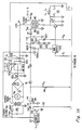
- FIGURE 1 illustrates a portion of a television receiver incorporating a deflection IC 100, embodying the invention.
- Such portion of the television receiver includes a bridge rectifier 101 that rectifies a mains supply voltage V AC to produce a DC, unregulated voltage V UR .
- a conventional power supply output stage or switch regulator 102 that may include a silicon controlled rectifier (SCR) produces during a normal operation power-up mode a regulated voltage B+ that is coupled to a flyback transformer T1.
- An input supply terminal 102c of regulator 102 is coupled to unregulated voltage V UR .
- Regulated voltage B+ is developed at an output terminal 102d of switch regulator 102.
- Transformer T1 is coupled to a collector electrode of a deflection switching transistor Q1 of a horizontal circuit output stage 99 operating at a horizontal rate f H .
- a control signal H r at the horizontal rate f H , that is produced in a corresponding portion of deflection IC 100, referred to herein as a horizontal processor 100a (Fig. 1B), is coupled via a horizontal driver 666 to the base electrode of transistor Q1.
- the frequency of signal H r is determined by a horizontal oscillator, not shown in the FIGURES, that may be included in IC 100.
- Signal H r controls the switching of transistor Q1 to generate a deflection current i y in a deflection winding L Y of output stage 99.
- a retrace voltage V w2 is produced in a conventional manner across a winding W2 of transformer T1 in each retrace interval of each horizontal period H.
- a second retrace voltage H in in a winding W3 of transformer T1 that is coupled to horizontal processor 100a is used in synchronizing deflection current i y to a synchronizing signal H s .
- Signal H s is generated in a sync separator, not shown in the FIGURES.
- a run supply voltage V+ is produced by rectifying voltage V w2 in a rectifier arrangement 104 that is coupled to winding W2.
- DC Voltage V+ is coupled to a corresponding portion of deflection IC 100, that is referred to herein as switch mode regulator processor 100b, to provide a feedback signal V IN .
- Processor 100b generates a pulse width modulated signal S c that controls the duration, in each horizontal interval H, in which switch regulator 102 is conductive.
- the duty cycle of signal S c varies, in accordance with a difference between the feedback signal, that is proportional to voltage V+, and a reference voltage V NIN that may be produced in a conventional manner.
- Signal S c causes regulated voltage B+ to be at a predetermined DC voltage level such as, illustratively, +125 volts.
- Signal S c , voltage B+ and voltage V+ are produced, illustratively, when deflection IC 100 operates in the power-up mode but are not produced during television receiver standby mode operation.
- Voltage V+ is coupled to a voltage divider 605 that includes series coupled resistors 601, 604 and 602.
- Resistor 604 includes a wiper k for developing a voltage that is representative of, for example, voltage B+.
- the voltage at wiper k that is adjustable by varying the position of wiper k, is coupled to an inverting input terminal 608 of an error amplifier 610 via a resistor 607.
- An integrating lowpass filter is coupled between inverting input terminal 608 and an output terminal 610a of amplifier 610 to provide the loop filter of regulator processor 100b.
- a filtered error voltage V0 developed at terminal 610a, is coupled to a pulse width modulator 100b(1), that produces pulse width modulated signal S c .
- Signal S c is coupled to a control terminal 102a of switch regulator 102 to turn on a pass switch 102b for a duration, in each period H, that varies in accordance with the duty cycle of signal S c .
- the duration, during each horizontal period H, in which switch 102b conducts, that is controlled by signal S c is determined by the level of error voltage V0 of error amplifier 610.
- the level of each of regulated voltages B+ and V+ is determined by a reference voltage V NIN that is produced in a conventional manner, not shown in the FIGURES.
- a standby transformer T0 steps down voltage V AC .
- the stepped down voltage is rectified in a rectifier arrangement 106 to produce a standby voltage V SB .
- Standby voltage V SB is coupled to an energizing voltage receiving terminal 120 of deflection IC 100 through a resistor R1 that charges a capacitor 66, during, for example, the standby mode operation, to produce in capacitor 66 an energizing voltage V cc at terminal 120 of deflection IC 100.
- Regulated voltage V+ is coupled to terminal 120 via a diode D2 and resistor 150 to supply voltage V cc from voltage V+ when deflection IC 100 operates in the power-up mode but not when the standby mode operation occurs.
- Standby voltage V SB is coupled to a remote receiver 107 to provide the operating voltage of remote receiver 107.
- Remote receiver 107 is coupled via an MOS transistor 108 to IC 100.
- transistor 108 When transistor 108 is conductive, a low impedance is formed between a junction terminal 109 of a resistor R734 and ground. The low impedance occurs after, for example, a user initiates a power-on command via an infra-red communication link that causes a start-up interval to occur, as described later on.
- the television receiver In the power-up mode that follows the start-up interval, the television receiver is fully operative. Conversely, after a power-off command is initiated by the user, transistor 108 becomes nonconductive and forms a high impedance circuit at terminal 109 that causes a standby mode to occur. In the standby mode the raster scanning on a display device of the television receiver is turned-off.
- a transistor Q705 operating as a constant current source, has its collector coupled to junction terminal 109.
- an on/off signal 110 is developed.
- Signal 110 is at a high level, or a second state, when transistor 108 is noncoductive, that corresponds to operation in the standby off-mode, and at a low level, or a first state, when it is conductive, that corresponds with operation in the power-up on-mode.
- An input supply current i PS is coupled through terminal 120 to deflection IC 100 for providing the energizing current of deflection IC 100.
- current i PS is supplied mainly by rectifier arrangement 104 through diodes D2 and D4; whereas, during operation in the standby mode, current i PS is supplied from standby transformer 106 via rectifier arrangement 106 and resistor R1.
- Voltage V cc is regulated in deflection IC 100 by a shunt regulator 131 that may be required to regulate voltage V cc during operation in both the standby mode and the power-up mode. Regulation of voltage V cc during the standby mode may be desirable for protecting deflection IC 100 from an overvoltage condition at terminal 120 that may occur should voltage V cc exceed the voltage rating of deflection IC 100. If permitted to occur, such overvoltage condition may damage deflection IC 100. Also regulation of voltage V cc during the standby mode may be desirable for operating circuitry in deflection IC 100 that may be required to operate during the standby mode such as, for example, transistor Q705.
- Shunt regulator 131 regulates voltage V cc in accordance with a reference voltage V BG2 that is generated during both the power-up and standby modes.
- Voltage V BG2 is generated in, for example, a bandgap type voltage source 105 that is, therefore, required to operate during both the standby and the power-up modes.
- Deflection IC 100 includes various circuit portions that, unlike shunt regulator 131 and bandgap voltage source 105, need not be energized during operation in the standby mode. For example, each of horizontal processor 100a and regulator processor 100b need not be energized during operation in the standby mode.
- Reducing the level of current i PS that is supplied from standby transformer T0 during the standby mode and the start-up interval is desirable in order to relax the specifications of transformer T0 so as to reduce its cost.
- cost is related to the current requirement imposed on transformer T0 that is directly related to current i PS .
- a circuit portion of deflection IC 100 may include a first plurality of transistors. Such arrangement is depicted by transistors 90a-90n of the P-N-P type. Each such transistor may be arranged in a common base configuration to form at the collector of such transistor a current source having a high output impedance. Each of transistors 90a-90n has its base electrode coupled to a common conductor that is referred to as PNP bus 11. It should be understood that some of transistors 90a-90n may be included in, for example, horizontal driver 100a and some others in regulator processor 100b.
- Transistor 90f illustrates one typical example of a circuit stage that is formed by a corresponding one of transistors 90a-90n. In such stage, a collector current i 90f is coupled to circuitry that is symbolically referred to as load circuit 90f1.
- a second typical example is shown in the arrangement of amplifier 610 that is included in regulator processor 100b.
- Amplifier 610 of FIGURE 1 forms a differential amplifier in which transistor 90n provides a current i 90n that is coupled to the emitters of transistors 90n2 and 90n3 of differential amplifier 610.
- Output voltage V0 of FIGURES 1 and 2 is developed at the collector of transistor 90n3 of FIGURE 1.
- the collector current in each of transistors 90a-90n is controlled by a voltage V BR that is coupled, via PNP bus 11, to the corresponding base electrode of each of transistors 90a-90n and that is generated by a temperature compensated current control arrangement 300.
- the emitter electrodes of the above-mentioned transistors 90a-90n are coupled through corresponding resistors to supply voltage V cc that is, as described before, a fixed DC voltage. Because of such arrangement, the collector currents in each of transistors 90a-90n track each other over a wide range of temperature to form a current mirror arrangement.
- Current control arrangement 300 controls voltage V BR in such a way that the collector current in each of transistors 90a-90n stays substantially constant when the temperature changes.
- Current control arrangement 300 includes transistors 90a, 90b, 73, 76, 77 and 80.
- the collector of transistor 73 is grounded.
- the collector of transistor 90a is coupled to the base of transistor 73 and, at a terminal 300c, to the collectors of transistors 76 and 77.
- the emitter of transistor 77 is coupled to a terminal 300a via a resistor R61.
- the emitter of transistor 76 is coupled to the base of transistor 77, to the base of transistor 80 and, via a resistor R60, to terminal 300a.
- Transistor 80 is arranged in a common emitter configuration.
- the base of transistor 76 is coupled, at a terminal 300b, to the collectors of both transistor 80 and 90b.
- the emitter of transistor 80 is coupled to terminal 300a.
- Transistors 76, 77 and 80 form a temperature compensating feedback network that controls via transistor 73 voltage V BR and maintains constant currents i 90a and i 90b in respective transistor 90a and 90b
- Transistor 76 forms, with transistor 80, a feedback arrangement that causes a collector current i 90b of transistor 90b to flow also as a collector current in transistor 80, by developing the corresponding base-emitter voltage in transistor 80 and across resistor R60. As described later on, current i 90b is maintained constant over a wide range of temperatures.
- transistor 77 is coupled with its base to sensing resistor R60.
- the current in resistor R60 is proportional to the voltage across the base-emitter junction of transistor 80 that varies inversely with temperature. Whereas, for a given voltage across resistor R60, the voltage across resistor R61 that determines the collector current in transistor 77 varies directly with the temperature.
- variations of the base-emitter forward voltages of transistors 77 and 80 have opposite effects on the sum of the currents in resistors R60 and R61 that causes, via a feedback arrangement, a collector current i 90a in transistor 90a to be substantially constant when the temperature varies.
- collector current i 90a flowing through terminal 300c that is approximately equal to the sum of the currents in the collectors of transistors 76 and 77 or in resistors R60 and R61, is maintained constant throughout a wide range of operating temperatures. Because of the feedback arrangement of transistor 73, voltage V BR causes the corresponding collector current in each of the other ones of transistors 90a-90n to be also temperature independent.
- Terminal 300a is coupled to an I2L injector line 12 that provides a temperature compensated injection current that is equal to the sum of currents i 90a and i 90b to a portion of deflection IC 100 that utilizes the well known I2L technology.
- Transistors 290a-290j, that are coupled to line 12, represent the injector transistors of such portion of deflection IC 100.
- transistors 190a-190m of the N-P-N type that may be utilized in various stages of deflection IC 100.
- Each of transistors 190a-190m has its base electrode coupled to a common conductor, or rail line, that is referred to as NPN bus 10 and has its emitter electrode coupled via a corresponding resistor to ground.
- Voltage V cc at terminal 120 is coupled to the collector of a transistor 81 which has its base coupled to the collector of transistor 90i.
- the emitter of transistor 81 is coupled to the base of a transistor 82 which is coupled back via its collector to the collector of transistor 90i.
- Transistors 81 and 82 produce a temperature compensated voltage V BR1 on bus 10 that performs a function analogous to voltage V BR of bus 11 and that is controlled by voltage V BR .
- voltage V BR1 enables the collector currents in transistors 190a-190m to flow only when voltage V BR enables the flow of the collector currents in transistors 90a-90n.
- Transistors 81 and 82 that are coupled to transistor 90i cause the collector current in each of transistors 190a-190m to be the current mirror of the collector current in transistor 90i that is controlled by voltage V BR , and therefore, temperature independent.
- Each of horizontal processor 100a and regulator processor 100b of FIGURE 1 that produce signals H r and S c , respectively, may include transistors from each of the groups 90a-90n, 190a-190m and 290a-290j.
- voltage V BR controls the operation of processor 100a and of regulator processor 100b.
- An example of a manner by which, during normal operation, transistors such as transistors 90a-90n and 190a-190m of FIGURE 1 may be used for generating control signals such as, for example, signals S c and H r is depicted in a data sheet for linear integrated circuits CA3210E and CA3223E of the RCA Corporation, published May, 1982, and entitled TV Horizontal/Vertical Countdown Digital Sync System .
- on/off signal 110 is coupled via an arrangement, operating as a signal inverter, that includes transistors Q700, Q701 and Q703, to a junction terminal 200a of an on/off switching arrangement 200.
- a second on/off control signal V 200a that is developed at junction terminal 200a is at a high level as a result of signal 110 being at the low level; conversely, during operation in the standby mode signal V 200a is at a low level.
- On/off switching arrangement 200 includes a zener diode 83 that has its cathode coupled to voltage V cc and its anode coupled via a resistor R202 to junction terminal 200a that is coupled to the bases of two switching transistors 84 and 85. Junction terminal 200a is coupled via a resistor 86 to ground.
- the emitter of switching transistor 84 that is conductive only during a short interval following a user initiated power-up command, referred to herein as the start-up interval, is coupled to bus 10 at a junction between the base of transistor 82 and the emitter of transistor 81.
- the collector of transistor 84 is coupled back to both collectors of transistors 76 and 77 of current control arrangement 300 at terminal 300c.
- the collector of switching transistor 85 is coupled to the bases of transistors 87 and 90 and to voltage V cc via a resistor 88 to turn-on transistors 87 and 90 when switching transistor 85 is nonconductive.
- the collector of transistor 87 is coupled back at terminal 300b to the base of transistor 76, to the collector of transistor 80 and to the collector of transistor 90b.
- control signal V 200a that is at the low level as a result of signal 110 being at the high level, causes transistor 87 to be in saturation. Consequently, a collector current i 90b of transistor 90b that flows into terminal 300b is shunted away from transistor 80 by transistor 87 that is conductive. Therefore, the collector current in each of transistors 76, 77 and 80 is forced to be zero. It follows that when on/off control signal 110 is at the high level, as a result of the user initiated power-off command, no base current flows in transistor 73 of arrangement 300. The emitter current in transistor 73 is, therefore, also zero.
- Voltage V BR is, during normal operation power-up mode, a temperature compensated voltage that causes the corresponding collector currents in transistors 90a-90n to be temperature compensated, as described before.
- voltage V BR causes the base current and, hence, the emitter current, in each of transistors 90a-90n, to be zero.
- temperature compensated arrangement 300 that generates temperature compensated voltage V BR couples on/off signal 110 to bus 11 to turn off transistors 90a-90n. Because the collector current in transistor 90i is zero, the emitter current in each of transistors 190a-190m is also zero. Also, because the emitter current in each of transistors 76, 77 and 80 is zero, I2L injector transistors 290a-290j become also nonconductive.
- control signal S c remains at an inactive state that prevents conduction of switch 102b so as to prevent the generation of voltage B+. It follows that during the standby mode, supply current i PS that flows in deflection IC 100 and that is proportional to the sum of the emitter currents in transistors 90a-90n, for example, is reduced relative to its value during the power-up mode. The result is that current loading of standby transformer TO is, advantageously, reduced during the standby mode.
- transistor 108 that is coupled to remote receiver 107, become conductive that causes signal 110 to be at the low level .
- transistor Q703 becomes nonconductive, due to signal 110 being at the low level, conductive zener diode 83 generates signal V 200a .
- Zener diode 83 is conductive as long as voltage V cc exceeds a predetermined minimum, or threshold, first level. Zener diode 83 prevents initiation of the start-up operation if capacitor 66 is not fully charged above the first level.
- On/off control signal V 200a at terminal 200a that is pulled up to a sufficiently high level by conductive zener 83 causes transistors 85 and 84 to become turned-on. With transistor 85 conducting, transistors 87 and 90 are turned off.
- transistor 84 draws current from the base of transistor 73, which begins to conduct simultaneously with transistor 84.
- Transistor 85 shunts the base currents of transistors 87 and 90, causing them to turn off.
- the conduction of transistor 73 causes transistors 90a, 90b and 90i to conduct the corresponding collector currents.
- Transistor 87 being turned off, allows the conduction of transistor 90b to turn on the feedback network comprising transistors 76, 77 and 80.
- Conduction of transistor 90i turns on transistors 81 and 82 that cause voltage V BR1 at the emitter of transistor 84 to increase. The increase in voltage V BR1 causes transistor 84 to become nonconductive.
- Transistor 73 base current is now supplied by conduction of transistors 76 and 77.
- current control arrangement 300 enables the emitter currents in each of transistors 90a-90n and 190a-190m to flow; thereby, deflection IC 100 that may include a horizontal oscillator, not shown in the FIGURES, becomes fully operational.
- signals H r and S c are generated and deflection switching transistor Q1 is switched on and off at the deflection rate f H , that initiates the generation of voltage V+.
- voltage V cc of deflection IC 100 is obtained during the power-up mode from voltage V+.
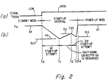
- FIGURES 2a and 2b illustrate schematically waveforms useful for explaining the operation of deflection IC 100 of FIGURE 1 during the start-up interval. Similar numbers and symbols in FIGURES 1, 2a and 2b depict similar items or functions.
- IC 100 of FIGURE 1 is powered primarily from the charge already stored in capacitor 66. Because of the loading caused by, for example, transistors 90a-90n, capacitor 66 may discharge prior to voltage V+ attaining its normal operational level. The result is that voltage V cc of FIGURE 2b may be reduced at, for example, time t1 to a level so low that voltage V cc is insufficient to sustain operation in the power-up mode. The discharge of capacitor 66 of FIGURE 1 may occur since deflection IC 100 may draw more current than can be provided by standby voltage V SB via resistor R1, that is relatively large valued. Resistor R1 is designed to be a large resistor so as to reduce loading of transformer T0 during the standby mode and start-up interval.
- zener diode 83 will turn off when capacitor 66 voltage falls below the breakdown zener voltage of diode 83.
- Transistor 85 remains, however, conductive, due to a supply of current through resistors 91 and 92.
- Deflection IC 100 will continue to operate to generate signals H r and S c until, for example, time t1 of FIGURE 2b when voltage V cc in capacitor 66 of FIGURE 1 falls below a second predetermined level VL2 of FIGURE 2b.
- the second predetermined level VL2 is a lower holding level of, for example, 4 volts, which is sufficient to supply enough current through resistors 91 and 92 of FIGURE 1 to maintain conduction of transistor 85.
- transistor 85 of FIGURE 1 turns off below the lower holding level that occurs at time t1 of FIGURE 2b.
- transistor 85 of FIGURE 1 turns off.
- transistors 87 and 90 will again saturate, thus turning off transistor 76 which will cause the emitter currents in transistors 90a-90n and 190a-190m to become zero, so as to terminate the start-up operation after time t1 of FIGURE 2b.
- Capacitor 66 may, therefore, be recharged as many times as are necessary until power-up operation is obtained, to cause voltage V+ to be operative so as to supply voltage V cc .
- deflection IC 100 of FIGURE 1 is essentially in an off condition with the load current sources disabled until capacitor 66 recharges to the first predetermined voltage such as level VL1 that occurs at time t2 of FIGURE 2b.
- a second start-up attempt occurs that is similar to that occurring during interval t0-t1.
- voltage V+ of FIGURE 1 becomes sufficiently large so as to begin charging capacitor 66 via diode D2.
- capacitor 66 of FIGURE 1 is charged up to a level that is controlled by shunt regulator 131 that occurs at time t4 of FIGURE 2b.
- start-up operation ceases and normal operation in a power-up mode begins. It should be understood that a successful start-up attempt that is not terminated may occur immediately after time t0 of FIGURE 2b when, for example, the amplitude of voltage V AC is sufficiently high.
- signal 110 is maintained at the low level, thereby maintaining signal V 200a at a high level.
- Transistors 87 and 84 are maintained nonconductive, and transistors 73, 76, 77 and 80 conductive. Consequently, normal operation emitter currents in transistors 90a-90n and 190a-190m, that are controlled by voltage V BR , and normal operation level of supply current i PS are maintained.
- voltage V BR on PNP bus 11 that is temperature compensated during the power-up mode, operates as a switching signal, during the standby mode.
- the emitter currents in transistors 90a-90n are, advantageously, switched off, during the standby mode.
Landscapes
- Engineering & Computer Science (AREA)
- Multimedia (AREA)
- Signal Processing (AREA)
- Dc-Dc Converters (AREA)
- Television Receiver Circuits (AREA)
- Details Of Television Scanning (AREA)
Claims (22)
- Dispositif de télévision capable de fonctionner sélectivement dans un mode d'attente et dans un mode sous tension , comprenant :
un circuit de déviation (99) pour produire un courant de déviation (iy) dans un enroulement de déviation (Ly) pendant le fonctionnement dudit dispositif de télévision dans un mode sous tension ;
une source (66) d'une première tension d'alimentation (Vcc) qui est développée pendant le fonctionnement dudit dispositif de télévision dans chacun desdits modes d'attente et sous tension ;
un circuit de commande (IC 100) couplé audit circuit de déviation (99) pour commander le fonctionnement dudit circuit de déviation pendant le fonctionnement dans ledit mode sous tension et pour empêcher la production dudit courant de déviation pendant le fonctionnement dans ledit mode d'attente, ledit circuit de commande comprenant au moins un premier étage de circuit (90a) qui est couplé pendant le fonctionnement dans chacun desdits modes d'attente et sous tension à ladite source (66) de ladite première tension d'alimentation (Vcc) pour former un trajet de courant dans lequel une première partie d'un courant d'alimentation circule à partir de ladite source (66) de ladite première tension d'alimentation (Vcc) pendant le fonctionnement dans ledit mode sous tension;
une source (107) d'un signal de commande de marche/arrêt (110) qui est sélectivement indicateur du fonctionnement dudit dispositif de télévision dans ledit mode sous tension et dans ledit mode d'attente ; caractérisé par
un moyen (300) couplé à ladite source (107) dudit signzl de commande de marche/arrêt (110) pour générer pendant le fonctionnement dudit dispositif de télévision un second signal de commande (VBR) dont la valeur est sensiblement invariable avec la température et qui est appliqué audit premier étage de circuit (90a) pour contrôler ladite première partie (i90a) dudit courant d'alimentation (ips) d'une façon qui est à compensation thermique , ledit moyen pour générer un signal à compensation thermique étant sensible audit signal de commande de marche/arrêt (110) de telle sorte que, pendant le fonctionnement dudit dispositif de télévision dans ledit mode d'attente, ledit signal de commande de marche/arrêt entraine ledit second signal de commande à compensation thermique (VBR) à réduire ladite première partie (i90a) dudit courant d'alimentation (ips) qui circule dans ledit premier étage de circuit (90a). - Dispositif selon la revendication 1, caractérisé par une première pluralité d'étages de circuit (90b-90a) qui forme des trajets de courant correspondant aux différentes parties correspondantes dudit courant d'alimentation (ips) de telle sorte que ledit second signal de commande (VBR) qui est couplé à chaque étage de ladite pluralité d'étages de circuit (90b-90a) provoque séparément une réduction correspondante de chacune desdites différentes parties de courant dans chacun desdits étages de circuit (90b-90a).
- Dispositif selon la revendication 1, caractérisé en ce que ledit circuit de déviation (99) inclut un transformateur de retour de balayage (TI) pour produire une seconde tension d'alimentation (V4) à partir dudit transformateur de retour et dans lequel ladite source (66) de ladite première tension d'alimentation (Vcc) développe ladite première tension d'alimentation à partir de ladite seconde tension d'alimentation (V4) pendant ledit mode sous tension.
- Dispositif selon la revendication 1 caractérisé en ce que ledit circuit de commande (IC 100) est couplé audit circuit de déviation (99) pour produire un signal (Hr) relié à la fréquence de déviation pour contrôler les rythmes dudit courant de déviation (iy) dans ledit enroulement de déviation (Ly).
- Dispositif selon la revendication 4 caractérisé par un moyen réglable (102) pour générer une seconde tension d'alimentation (B4) dans lequel ledit circuit de commande (IC 100) produit de plus un signal de commande modulé en largeur d'impulsion (Sc) qui est couplé audit moyen de production de la seconde tension d'alimentation (102) pour commander ladite seconde tension d'alimentation pendant ledit mode sous tension et pour invalider ladite seconde tension d'alimentation (B4) pendant ledit mode d'attente .
- Dispositif selon la revendication 5 caractérisé en ce que ladite seconde tension d'alimentation (B4) est couplée audit circuit de déviation (99) pour fournir une partie importante de la demande totale d'énergie dudit circuit de déviation (99).
- Dispositif selon la revendication 1 caractérisé en ce que ledit premier étage de circuit comprend un premier transistor (90a) comportant une première électrode conductrice de courant principal (émetteur) qui est couplée à ladite cource (66) de la première tension d'alimentation (Vcc) et qui est, de ce fait, excitée pendant lesdits modes sous tension et d'attente de telle sorte que ladite première partie (i90a) dudit courant d'alimentation (ips) circule à partir de ladite source (66) de la première tension d'alimentation (Vcc) dans ladite première électrode conductrice de courant principal pendant ledit mode sous tension et dans lequel ledit second signal de commande (VBR) est couplé à une électrode de commande (base) dudit premier transistor (90a).
- Dispositif selon la revendication 7 caractérisé en ce que ledit second signal de commande (VBR) entraine ledit premier transistor (90a) à fonctionner comme un commutateur qui est non conducteur lorsque le signal de commande de marche/arrêt (110) est indicateur du fonctionnement dans ledit mode d'attente.
- Dispositif selon la revendication 7 caractérisé en ce que ledit circuit de commande (IC 100) comprend une première pluralité de transistors (90b-90n) comportant des électrodes de commande (bases) qui sont couplées audit signal de commande de marche/arrêt via un trajet incluant un conducteur commun (pour VBR) qui entraine un courant correspondant dans chaque transistor de ladite première pluralité de transistors (90b-90n) à devenir le miroir de courant dudit courant dans ledit transistor (90a) qui est à compensation thermique.
- Dispositif selon la revendication 9 caractérisé en ce que chaque transistor de ladite première pluralité de transistors (90b-90n) fonctionne comme une source de courant pour produire une partie de courant correspondante dans leur électrode conductrice de courant principal correspondante seulement pendant ledit mode sous tension.
- Dispositif selon la revendication 1 caractérisé en ce que ledit moyen (300) pour générer ledit second signal de commande (VBR) comprend un agencement de circuit (290a-290j) qui demande un courant d'injection (I²L) (logique d'injection intégrée) pour un fonctionnement pendant ledit mode sous tension et dans lequel ledit moyen (300) pour générer ledit second signal de commande (VBR) est couplé audit agencement de circuit (290a-290j) pour fournir ledit courant d'injection I²L qui est à compensation thermique de telle sorte que ledit moyen (300) pour générer ledit second signal de commande (VBR) empêche ledit courant d'injection I²L de circuler pendant ledit mode d'attente.
- Dispositif selon la revendication 1 caractérisé en ce que ledit moyen (300) pour générer ledit second signal de commande (VBR) comprend une source de tension dépendante de la température qui est proportionnelle à une tension établie à travers une première structure de jonction P-N conductrice (base émetteur de 80) , une première résistance (R 60) couplée en parallèle à ladite source de tension dépendante de la température pour extraire un courant à une valeur qui est en conformité avec ladite tension à travers ladite première structure de jonction P-N, une seconde structure de jonction P-N (base -émetteur de 77) et une seconde résistance (61) qui forment avec ladite seconde structure de jonction P-n, un agencement en série qui est couplé en parallèle à ladite première résistance (R60) pour conduire un courant dans ladite seconde résistance (R 61) qui est en conformité avec ladite tension à travers ladite première structure de jonction P-N (base émetteur de 80), ledit courant dans ladite seconde résistance (R61) ayant un coefficient de variation de température qui est proportionnel à la valeur négative du coefficient de variation de température dudit courant dans ladite première résistance (R 60) qui compense sensiblement ledit coefficient de température dudit courant dans ladite première résistance (R 60) sur une large gamme de températures de fonctionnement, et un circuit de réaction (73) sensible à la somme desdits courants dans lesdites première (R 60) et seconde (R 61) résistances afin de développer ledit second signal de commande (VBR) pour fournir une tension de commande à compensation thermique qui est couplée à une électrode de commande (base) d'un premier transistor (90a) qui est inclus dans ledit premier étage de circuit.
- Dispositif selon la revendication 12 caractérisé en ce que ledit circuit de réaction comprend un second transistor (73) comportant une électrode conductrice du courant principal (émetteur) qui est couplée à ladite électrode de commande (base) dudit premier transistor (90a) et dans lequel ledit courant dans ledit premier transistor (90a) , ledit courant dans ladite première résistance (R60) et ledit courant dans ladite seconde résistance (R 61) sont combinés au niveau d'une électrode de commande (base) dudit second transistor (73) pour développer à ce niveau une tension qui est couplée à ladite électrode de commande (base) dudit premier transistor (90A) via ladite électrode conductrice du courant principal (émetteur) dudit second transistor (73).
- Dispositif selon la revendication 1 caractérisé en ce que ledit circuit de commande (IC 100) comprend, de plus, une pluralité de transistors (90b-90n) chaque transistor de ladite pluralité de transistors ayant une électrode de commande (base) qui est couplée à un borne conductrice de courant (émetteur) dudit premier étage de circuit (90a) de telle sorte qu'un courant correspondant dans chaque transistor de ladite pluralité de transistors (90a-90n) est le miroir de courant dudit courant dudit premier étage de circuit (90a) qui provoque une réduction correspondante dudit courant correspondant dans chacun desdits transistors de ladite pluralité de transistors pendant ledit mode d'attente.
- Dispositif selon la revendication 1 caractérisé en ce que ladite source de la première tension d'alimentation (Vcc) comprend une source (VAc) de tension d'alimentation CA (courant alternatif), un transformateur d'abaissement de tension (TO) couplé à ladite source de tension d'alimentation CA, un redresseur (D 106) ayant une borne d'entrée qui est couplée audit transformateur d'abaissement de tension pour produire une tension d'alimentation d'attente (VSB) en redressant une tension qui est développée audit transformateur d'abaissement de tension qui fournit ledit courant d'alimentation (ips) pendant ledit mode d'attente.
- Dispositif selon la revendication 15 caractérisé par une source (104) d'une seconde tension d'alimentation (V4) qui est développée pendant ledit mode sous tension et un moyen (D2) pour coupler sélectivement ladite tension d'alimentation d'attente (VSB) à une borne de connexion d'entrée (120) dudit circuit de commande (IC 100) pendant ledit mode d'attente et pour coupler sélectivement ladite seconde tension d'alimentation (V4) pendant leditmode sous tension de façon à produire ladite première tension d'alimentation (Vcc) à ladite borne de connexion d'entrée (120) pendant les deux dits modes sous tension et d'attente.
- Dispositif selon la revendication 16 caractérisé en ce que ladite source (104) de la seconde tension d'alimentation (V4) comprend un enroulement (Wz) d'un transformateur de retour de balayage (T1) couplé audit circuit de déviation (99) et un redresseur (D4) couplé audit enroulement (Wz) pour fournir ladite seconde tension d'alimentation (V4) seulement pendant ledit mode sous tension.
- Dispositif selon la revendication 15 caractérisé en ce que ledit second signal de commande (VBR) entraine une réduction du courant qui circule dans ledit premier transformateur d'abaissement de tension (TO) pendant ledit mode d'attente.
- Dispositif selon la revendication 1 caractérisé en ce que ladite source (109) dudit ignal de commande de marche/arrêt (110) comprend un récepteur à distance dudit dispositif de télévision.
- Dispositif selon la revendication 1 caractérisé en ce que ledit circuit de commande (IC 100) inclut, de plus, une partie de circuit (131, 200) qui est couplée à ladite première tension d'alimentation (Vcc) et qui est excitée , de ce fait, pendant les deux dits modes sous tension et d'attente.
- Dispositif selon la revendication 20 caractérisé ence que ladite partie de circuit comprend un régulateur en dérivation (131) qui régule ladite première tension d'alimentation (Vcc) .
- Dispositif selon la revendication 1 caractérisé en ce que ledit circuit de commande (IC 100) forme un circuit intégré et dans lequel ladite première tension d'alimentation (Vcc) est appliquée à une borne de connexion d'entrée (120) pendant les deux dits modes sous tension et d'attente.
Applications Claiming Priority (2)
| Application Number | Priority Date | Filing Date | Title |
|---|---|---|---|
| US07/042,077 US4737851A (en) | 1987-04-24 | 1987-04-24 | On/off control circuitry for television |
| US42077 | 1987-04-24 |
Publications (3)
| Publication Number | Publication Date |
|---|---|
| EP0288312A2 EP0288312A2 (fr) | 1988-10-26 |
| EP0288312A3 EP0288312A3 (en) | 1990-03-14 |
| EP0288312B1 true EP0288312B1 (fr) | 1993-11-10 |
Family
ID=21919916
Family Applications (1)
| Application Number | Title | Priority Date | Filing Date |
|---|---|---|---|
| EP88303669A Expired - Lifetime EP0288312B1 (fr) | 1987-04-24 | 1988-04-22 | Circuit de commande de marche/arrêt pour télévision |
Country Status (7)
| Country | Link |
|---|---|
| US (1) | US4737851A (fr) |
| EP (1) | EP0288312B1 (fr) |
| JP (1) | JP2944667B2 (fr) |
| KR (1) | KR960013733B1 (fr) |
| CA (1) | CA1288861C (fr) |
| DE (1) | DE3885496T2 (fr) |
| FI (1) | FI86238C (fr) |
Cited By (1)
| Publication number | Priority date | Publication date | Assignee | Title |
|---|---|---|---|---|
| US6114817A (en) * | 1998-08-07 | 2000-09-05 | Thomson Licensing S.A. | Power Supply for a deflection circuit operating at multi-scan frequencies |
Families Citing this family (11)
| Publication number | Priority date | Publication date | Assignee | Title |
|---|---|---|---|---|
| FR2607991B1 (fr) * | 1986-12-05 | 1989-02-03 | Radiotechnique Ind & Comm | Alimentation a decoupage pour un televiseur muni d'un systeme de veille |
| US4868466A (en) * | 1988-03-29 | 1989-09-19 | Rca Licensing Corporation | Power supply for a television apparatus |
| US5036261A (en) * | 1989-08-11 | 1991-07-30 | Thomson Consumer Electronics, Inc. | Standby/run power supply and control circuit |
| GB9113924D0 (en) * | 1991-06-27 | 1991-08-14 | Thomson Consumer Electronics | Fault protection using microprocessor power up reset |
| GB9114354D0 (en) * | 1991-07-03 | 1991-08-21 | Thompson Consumer Electronics | Run/standby control with switched mode power supply |
| US6018804A (en) * | 1996-03-25 | 2000-01-25 | Thomson Consumer Electronics, Inc. | Data bus isolator |
| JP6009734B2 (ja) * | 2008-02-05 | 2016-10-19 | フィリップス ライティング ホールディング ビー ヴィ | 受信ユニットの電力消費を制御する方法 |
| US20100053440A1 (en) * | 2008-09-01 | 2010-03-04 | Peter Mortensen | Television fast power up mode |
| US10270630B2 (en) | 2014-09-15 | 2019-04-23 | Analog Devices, Inc. | Demodulation of on-off-key modulated signals in signal isolator systems |
| US10536309B2 (en) * | 2014-09-15 | 2020-01-14 | Analog Devices, Inc. | Demodulation of on-off-key modulated signals in signal isolator systems |
| CN111247730B (zh) | 2017-10-17 | 2024-09-10 | 昕诺飞控股有限公司 | Ac/dc转换器、灯具以及提供改进的启动电路的方法 |
Family Cites Families (13)
| Publication number | Priority date | Publication date | Assignee | Title |
|---|---|---|---|---|
| US4188641A (en) * | 1978-07-28 | 1980-02-12 | Gte Sylvania Incorporated | Startup circuit for a television receiver |
| US4240013A (en) * | 1979-05-29 | 1980-12-16 | Rca Corporation | Horizontal deflection and power supply circuit with a start-up arrangement |
| US4301394A (en) * | 1979-11-28 | 1981-11-17 | Rca Corporation | Horizontal deflection circuit and power supply with regulation by horizontal output transistor turn-off delay control |
| US4429259A (en) * | 1980-09-12 | 1984-01-31 | Rca Corporation | Horizontal deflection circuit with a start-up power supply |
| US4385264A (en) * | 1981-05-07 | 1983-05-24 | Rca Corporation | Start-up circuit for a power supply |
| US4377775A (en) * | 1981-07-29 | 1983-03-22 | Rca Corporation | Television receiver ferroresonant power supply disabling circuit |
| US4532457A (en) * | 1982-01-29 | 1985-07-30 | Rca Corporation | Television receiver standby circuit |
| US4481564A (en) * | 1982-09-09 | 1984-11-06 | Zenith Electronics Corporation | Switched-mode power supply |
| US4500923A (en) * | 1982-10-29 | 1985-02-19 | Rca Corporation | Television receiver standby power supply |
| US4516168A (en) * | 1982-11-30 | 1985-05-07 | Rca Corporation | Shutdown circuit for a switching regulator in a remote controlled television receiver |
| DE3341074A1 (de) * | 1983-11-12 | 1985-05-23 | Telefunken Fernseh Und Rundfunk Gmbh, 3000 Hannover | Schaltnetzteil, insbesondere fuer einen fernsehempfaenger, mit einer schutzschaltung zur begrenzung des primaerstroms |
| US4651214A (en) * | 1984-12-24 | 1987-03-17 | Rca Corporation | Remote controlled television receiver power supply |
| US4692852A (en) * | 1986-06-25 | 1987-09-08 | Rca Corporation | Switching power supply with raster width stabilization |
-
1987
- 1987-04-24 US US07/042,077 patent/US4737851A/en not_active Expired - Lifetime
-
1988
- 1988-04-18 FI FI881796A patent/FI86238C/fi not_active IP Right Cessation
- 1988-04-21 CA CA000564736A patent/CA1288861C/fr not_active Expired - Fee Related
- 1988-04-22 KR KR88004572A patent/KR960013733B1/ko not_active Expired - Fee Related
- 1988-04-22 DE DE88303669T patent/DE3885496T2/de not_active Expired - Fee Related
- 1988-04-22 EP EP88303669A patent/EP0288312B1/fr not_active Expired - Lifetime
- 1988-04-22 JP JP63101205A patent/JP2944667B2/ja not_active Expired - Fee Related
Cited By (1)
| Publication number | Priority date | Publication date | Assignee | Title |
|---|---|---|---|---|
| US6114817A (en) * | 1998-08-07 | 2000-09-05 | Thomson Licensing S.A. | Power Supply for a deflection circuit operating at multi-scan frequencies |
Also Published As
| Publication number | Publication date |
|---|---|
| JPS63292879A (ja) | 1988-11-30 |
| FI86238C (fi) | 1992-07-27 |
| EP0288312A3 (en) | 1990-03-14 |
| FI86238B (fi) | 1992-04-15 |
| CA1288861C (fr) | 1991-09-10 |
| DE3885496D1 (de) | 1993-12-16 |
| JP2944667B2 (ja) | 1999-09-06 |
| KR960013733B1 (en) | 1996-10-10 |
| DE3885496T2 (de) | 1994-05-11 |
| US4737851A (en) | 1988-04-12 |
| EP0288312A2 (fr) | 1988-10-26 |
| FI881796A7 (fi) | 1988-10-25 |
| FI881796A0 (fi) | 1988-04-18 |
| KR880013394A (ko) | 1988-11-30 |
Similar Documents
| Publication | Publication Date | Title |
|---|---|---|
| US4734771A (en) | Start-up control circuitry for a television apparatus | |
| US4941078A (en) | Synchronized switch-mode power supply | |
| US4737851A (en) | On/off control circuitry for television | |
| CA2001907C (fr) | Regulateur de tension pour televiseur | |
| US4761723A (en) | Power supply regulator for television | |
| KR0169317B1 (ko) | 액티브 턴 오프하는 전압 레귤레이터 | |
| CA1185362A (fr) | Circuit d'excitation pour bloc d'alimentation | |
| CA1309171C (fr) | Circuit de commande d'alimentation pour televiseur | |
| EP0527328B1 (fr) | Mise en marche lente dans un circuit de déflexion | |
| KR100225311B1 (ko) | 스위칭형 전원 장치 | |
| KR970006662B1 (ko) | 텔레비젼 장치 및 그 전원 | |
| US4812719A (en) | High voltage regulator in a television apparatus | |
| US4377775A (en) | Television receiver ferroresonant power supply disabling circuit | |
| CA1290447C (fr) | Stabilisateur d'alimentation electrique pour televiseur | |
| EP0972342B1 (fr) | Circuit pour commander un transistor de commutation | |
| KR19990055312A (ko) | 모니터의 트리거신호 공급회로 | |
| HK1004046B (en) | A power supply for a television apparatus | |
| JPH06292358A (ja) | スイッチング電源装置 |
Legal Events
| Date | Code | Title | Description |
|---|---|---|---|
| PUAI | Public reference made under article 153(3) epc to a published international application that has entered the european phase |
Free format text: ORIGINAL CODE: 0009012 |
|
| AK | Designated contracting states |
Kind code of ref document: A2 Designated state(s): DE FR GB |
|
| PUAL | Search report despatched |
Free format text: ORIGINAL CODE: 0009013 |
|
| AK | Designated contracting states |
Kind code of ref document: A3 Designated state(s): DE FR GB |
|
| 17P | Request for examination filed |
Effective date: 19900824 |
|
| RAP1 | Party data changed (applicant data changed or rights of an application transferred) |
Owner name: RCA THOMSON LICENSING CORPORATION |
|
| 17Q | First examination report despatched |
Effective date: 19920603 |
|
| GRAA | (expected) grant |
Free format text: ORIGINAL CODE: 0009210 |
|
| AK | Designated contracting states |
Kind code of ref document: B1 Designated state(s): DE FR GB |
|
| REF | Corresponds to: |
Ref document number: 3885496 Country of ref document: DE Date of ref document: 19931216 |
|
| ET | Fr: translation filed | ||
| PLBE | No opposition filed within time limit |
Free format text: ORIGINAL CODE: 0009261 |
|
| STAA | Information on the status of an ep patent application or granted ep patent |
Free format text: STATUS: NO OPPOSITION FILED WITHIN TIME LIMIT |
|
| 26N | No opposition filed | ||
| REG | Reference to a national code |
Ref country code: GB Ref legal event code: 732E |
|
| REG | Reference to a national code |
Ref country code: GB Ref legal event code: IF02 |
|
| REG | Reference to a national code |
Ref country code: FR Ref legal event code: D6 |
|
| REG | Reference to a national code |
Ref country code: GB Ref legal event code: 746 Effective date: 20030228 |
|
| PGFP | Annual fee paid to national office [announced via postgrant information from national office to epo] |
Ref country code: DE Payment date: 20050418 Year of fee payment: 18 |
|
| PGFP | Annual fee paid to national office [announced via postgrant information from national office to epo] |
Ref country code: FR Payment date: 20050425 Year of fee payment: 18 |
|
| PGFP | Annual fee paid to national office [announced via postgrant information from national office to epo] |
Ref country code: GB Payment date: 20060303 Year of fee payment: 19 |
|
| PG25 | Lapsed in a contracting state [announced via postgrant information from national office to epo] |
Ref country code: DE Free format text: LAPSE BECAUSE OF NON-PAYMENT OF DUE FEES Effective date: 20061101 |
|
| REG | Reference to a national code |
Ref country code: FR Ref legal event code: ST Effective date: 20061230 |
|
| GBPC | Gb: european patent ceased through non-payment of renewal fee |
Effective date: 20070422 |
|
| PG25 | Lapsed in a contracting state [announced via postgrant information from national office to epo] |
Ref country code: FR Free format text: LAPSE BECAUSE OF NON-PAYMENT OF DUE FEES Effective date: 20060502 Ref country code: GB Free format text: LAPSE BECAUSE OF NON-PAYMENT OF DUE FEES Effective date: 20070422 |