EP0291602A1 - Eléments de contact pour inductance miniature - Google Patents
Eléments de contact pour inductance miniature Download PDFInfo
- Publication number
- EP0291602A1 EP0291602A1 EP87308516A EP87308516A EP0291602A1 EP 0291602 A1 EP0291602 A1 EP 0291602A1 EP 87308516 A EP87308516 A EP 87308516A EP 87308516 A EP87308516 A EP 87308516A EP 0291602 A1 EP0291602 A1 EP 0291602A1
- Authority
- EP
- European Patent Office
- Prior art keywords
- inch
- inductor
- core
- copper
- contact elements
- Prior art date
- Legal status (The legal status is an assumption and is not a legal conclusion. Google has not performed a legal analysis and makes no representation as to the accuracy of the status listed.)
- Granted
Links
Images
Classifications
-
- H—ELECTRICITY
- H01—ELECTRIC ELEMENTS
- H01F—MAGNETS; INDUCTANCES; TRANSFORMERS; SELECTION OF MATERIALS FOR THEIR MAGNETIC PROPERTIES
- H01F17/00—Fixed inductances of the signal type
- H01F17/04—Fixed inductances of the signal type with magnetic core
- H01F17/06—Fixed inductances of the signal type with magnetic core with core substantially closed in itself, e.g. toroid
-
- H—ELECTRICITY
- H05—ELECTRIC TECHNIQUES NOT OTHERWISE PROVIDED FOR
- H05K—PRINTED CIRCUITS; CASINGS OR CONSTRUCTIONAL DETAILS OF ELECTRIC APPARATUS; MANUFACTURE OF ASSEMBLAGES OF ELECTRICAL COMPONENTS
- H05K3/00—Apparatus or processes for manufacturing printed circuits
- H05K3/30—Assembling printed circuits with electric components, e.g. with resistors
- H05K3/32—Assembling printed circuits with electric components, e.g. with resistors electrically connecting electric components or wires to printed circuits
- H05K3/34—Assembling printed circuits with electric components, e.g. with resistors electrically connecting electric components or wires to printed circuits by soldering
- H05K3/341—Surface mounted components
- H05K3/3431—Leadless components
- H05K3/3442—Leadless components having edge contacts, e.g. leadless chip capacitors, chip carriers
-
- H—ELECTRICITY
- H01—ELECTRIC ELEMENTS
- H01F—MAGNETS; INDUCTANCES; TRANSFORMERS; SELECTION OF MATERIALS FOR THEIR MAGNETIC PROPERTIES
- H01F27/00—Details of transformers or inductances, in general
- H01F27/28—Coils; Windings; Conductive connections
- H01F27/29—Terminals; Tapping arrangements for signal inductances
- H01F27/292—Surface mounted devices
-
- H—ELECTRICITY
- H05—ELECTRIC TECHNIQUES NOT OTHERWISE PROVIDED FOR
- H05K—PRINTED CIRCUITS; CASINGS OR CONSTRUCTIONAL DETAILS OF ELECTRIC APPARATUS; MANUFACTURE OF ASSEMBLAGES OF ELECTRICAL COMPONENTS
- H05K2201/00—Indexing scheme relating to printed circuits covered by H05K1/00
- H05K2201/09—Shape and layout
- H05K2201/09009—Substrate related
- H05K2201/09045—Locally raised area or protrusion of insulating substrate
-
- H—ELECTRICITY
- H05—ELECTRIC TECHNIQUES NOT OTHERWISE PROVIDED FOR
- H05K—PRINTED CIRCUITS; CASINGS OR CONSTRUCTIONAL DETAILS OF ELECTRIC APPARATUS; MANUFACTURE OF ASSEMBLAGES OF ELECTRICAL COMPONENTS
- H05K2201/00—Indexing scheme relating to printed circuits covered by H05K1/00
- H05K2201/10—Details of components or other objects attached to or integrated in a printed circuit board
- H05K2201/10431—Details of mounted components
- H05K2201/10568—Integral adaptations of a component or an auxiliary PCB for mounting, e.g. integral spacer element
-
- H—ELECTRICITY
- H05—ELECTRIC TECHNIQUES NOT OTHERWISE PROVIDED FOR
- H05K—PRINTED CIRCUITS; CASINGS OR CONSTRUCTIONAL DETAILS OF ELECTRIC APPARATUS; MANUFACTURE OF ASSEMBLAGES OF ELECTRICAL COMPONENTS
- H05K2201/00—Indexing scheme relating to printed circuits covered by H05K1/00
- H05K2201/10—Details of components or other objects attached to or integrated in a printed circuit board
- H05K2201/10613—Details of electrical connections of non-printed components, e.g. special leads
- H05K2201/10621—Components characterised by their electrical contacts
- H05K2201/10636—Leadless chip, e.g. chip capacitor or resistor
-
- Y—GENERAL TAGGING OF NEW TECHNOLOGICAL DEVELOPMENTS; GENERAL TAGGING OF CROSS-SECTIONAL TECHNOLOGIES SPANNING OVER SEVERAL SECTIONS OF THE IPC; TECHNICAL SUBJECTS COVERED BY FORMER USPC CROSS-REFERENCE ART COLLECTIONS [XRACs] AND DIGESTS
- Y02—TECHNOLOGIES OR APPLICATIONS FOR MITIGATION OR ADAPTATION AGAINST CLIMATE CHANGE
- Y02P—CLIMATE CHANGE MITIGATION TECHNOLOGIES IN THE PRODUCTION OR PROCESSING OF GOODS
- Y02P70/00—Climate change mitigation technologies in the production process for final industrial or consumer products
- Y02P70/50—Manufacturing or production processes characterised by the final manufactured product
Definitions
- This invention relates to miniature inductors and particularly to the securing of contact elements on the inductor so that the inductor can be surface mounted to a printed circuitboard.
- the inductor consists of a ferromagnetic core, a winding around the core, and contact elements to which the ends of the winding are soldered.
- the inductor is surface mounted to the copper pattern side of a printed circuitboard.
- the inductors to which the present invention is directed are tiny, having a maximum dimension of about 1/10 inch.
- An objective of the present invention has been to provide a mounting of a contact element to a miniature inductor that provides a good bond and significantly improves the Q of prior configurations.
- This objective is attained in accordance with the invention by using conventional printed circuitboard material as a contact element.
- the printed circuitboard material is a laminate of an impregnated fabric such as fiberglass forming a base and copper with tin plating covering the exposed surface of the copper.
- the preferred material is thin, being about 0.010 inch in thickness with the base being about 0.007 inch thick and the copper being from .001 inch to .003 inch thick.
- the base could be up to about .030 inch thick.
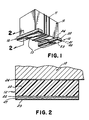
- Contact elements 12 are soldered to the contact elements.
- That inductor is suitable for surface mounting to the copper pattern of a printed circuitboard by soldering the contact elements to the copper on the printed circuitboard.
- the inductor is tiny. It has dimensions which will be set forth below. These dimensions will vary somewhat but are set forth here to provide the order of magnitude of size of inductor to which the present invention is applicable.
- the core is .100 to .250 inch long, .090 to .200 inch wide, and .050 to .150 inch high.
- the spacing between the contact elements 12 is about ..060 inch. Each contact element is about .020 inch wide and .070 inch to .200 inch long.
- the contact element 12 is formed from a laminate of an epoxy base fiberglass fabric 20 which is about .007 inch thick and copper 21 that is between .001 inch and .003 inch thick.
- the copper is bonded to the fiberglass by an adhesive 22 in accordance with the conventional practices in making printed circuitboard material.
- the copper is usually clad with a tin plate indicated at 23.
- Each contact element 12 is attached to the core 10 by means of an epoxy 24.
Landscapes
- Engineering & Computer Science (AREA)
- Power Engineering (AREA)
- Microelectronics & Electronic Packaging (AREA)
- Manufacturing & Machinery (AREA)
- Coils Or Transformers For Communication (AREA)
- Structures For Mounting Electric Components On Printed Circuit Boards (AREA)
Applications Claiming Priority (2)
| Application Number | Priority Date | Filing Date | Title |
|---|---|---|---|
| US07/052,070 US4725806A (en) | 1987-05-21 | 1987-05-21 | Contact elements for miniature inductor |
| US52070 | 1987-05-21 |
Publications (2)
| Publication Number | Publication Date |
|---|---|
| EP0291602A1 true EP0291602A1 (fr) | 1988-11-23 |
| EP0291602B1 EP0291602B1 (fr) | 1992-12-30 |
Family
ID=21975256
Family Applications (1)
| Application Number | Title | Priority Date | Filing Date |
|---|---|---|---|
| EP87308516A Expired - Lifetime EP0291602B1 (fr) | 1987-05-21 | 1987-09-25 | Eléments de contact pour inductance miniature |
Country Status (6)
| Country | Link |
|---|---|
| US (1) | US4725806A (fr) |
| EP (1) | EP0291602B1 (fr) |
| JP (1) | JPS63300505A (fr) |
| KR (1) | KR880014597A (fr) |
| CA (1) | CA1299258C (fr) |
| DE (1) | DE3783366T2 (fr) |
Cited By (1)
| Publication number | Priority date | Publication date | Assignee | Title |
|---|---|---|---|---|
| EP1598838A3 (fr) * | 2004-05-21 | 2006-04-19 | Minebea Co., Ltd. | Ensemble bobine et son procédé de fabrication |
Families Citing this family (9)
| Publication number | Priority date | Publication date | Assignee | Title |
|---|---|---|---|---|
| US4819130A (en) * | 1987-12-07 | 1989-04-04 | Harold Moy | Fail-safe radio frequency suppressor |
| USD329041S (en) | 1989-03-17 | 1992-09-01 | Tdk Corporation | Inductor for use in circuits for digital communications |
| DE19710462C2 (de) * | 1997-03-13 | 1999-05-20 | Siemens Matsushita Components | Elektrisches Bauelement, insbesondere Chipinduktivität |
| US6246311B1 (en) * | 1997-11-26 | 2001-06-12 | Vlt Corporation | Inductive devices having conductive areas on their surfaces |
| US6285272B1 (en) * | 1999-10-28 | 2001-09-04 | Coilcraft, Incorporated | Low profile inductive component |
| TW200743434A (en) * | 2006-05-11 | 2007-11-16 | Delta Electronics Inc | Packaged electronic component for shielding electromagnetic interference |
| TWD127897S1 (zh) * | 2007-09-19 | 2009-03-21 | 西鐵城電子股份有限公司 | 電感器 |
| JP1715053S (ja) * | 2021-07-26 | 2022-05-17 | コイル部品 | |
| JP1715052S (ja) * | 2021-07-26 | 2022-05-17 | コイル部品 |
Citations (1)
| Publication number | Priority date | Publication date | Assignee | Title |
|---|---|---|---|---|
| EP0175461A1 (fr) * | 1984-08-15 | 1986-03-26 | Standex International Corporation | Corps de bobine |
Family Cites Families (4)
| Publication number | Priority date | Publication date | Assignee | Title |
|---|---|---|---|---|
| US3550228A (en) * | 1967-11-29 | 1970-12-29 | Jean Claude Asscher | Method of assembling leads to an electrical component and potting same |
| US3585553A (en) * | 1970-04-16 | 1971-06-15 | Us Army | Microminiature leadless inductance element |
| DE2617465C3 (de) * | 1976-04-21 | 1978-10-19 | Siemens Ag, 1000 Berlin Und 8000 Muenchen | Elektrische Spule und Verfahren zu ihrer Herstellung |
| JPS5926577Y2 (ja) * | 1979-09-17 | 1984-08-02 | ティーディーケイ株式会社 | 小型インダクタンス素子 |
-
1987
- 1987-05-21 US US07/052,070 patent/US4725806A/en not_active Expired - Fee Related
- 1987-08-27 CA CA000545518A patent/CA1299258C/fr not_active Expired - Lifetime
- 1987-09-16 KR KR870010256A patent/KR880014597A/ko not_active Withdrawn
- 1987-09-25 DE DE8787308516T patent/DE3783366T2/de not_active Expired - Fee Related
- 1987-09-25 EP EP87308516A patent/EP0291602B1/fr not_active Expired - Lifetime
- 1987-10-21 JP JP62264062A patent/JPS63300505A/ja active Pending
Patent Citations (1)
| Publication number | Priority date | Publication date | Assignee | Title |
|---|---|---|---|---|
| EP0175461A1 (fr) * | 1984-08-15 | 1986-03-26 | Standex International Corporation | Corps de bobine |
Non-Patent Citations (1)
| Title |
|---|
| PATENT ABSTRACTS OF JAPAN, vol. 7, no. 236 (E-205)[1381], 20th October 1983; & JP-A-58 124 213 (SONY K.K.) 23-07-1983 * |
Cited By (2)
| Publication number | Priority date | Publication date | Assignee | Title |
|---|---|---|---|---|
| EP1598838A3 (fr) * | 2004-05-21 | 2006-04-19 | Minebea Co., Ltd. | Ensemble bobine et son procédé de fabrication |
| US7342475B2 (en) | 2004-05-21 | 2008-03-11 | Minebea Co., Ltd. | Coil arrangement and method for its manufacture |
Also Published As
| Publication number | Publication date |
|---|---|
| US4725806A (en) | 1988-02-16 |
| CA1299258C (fr) | 1992-04-21 |
| KR880014597A (ko) | 1988-12-24 |
| JPS63300505A (ja) | 1988-12-07 |
| DE3783366D1 (de) | 1993-02-11 |
| EP0291602B1 (fr) | 1992-12-30 |
| DE3783366T2 (de) | 1993-06-09 |
Similar Documents
| Publication | Publication Date | Title |
|---|---|---|
| US4725806A (en) | Contact elements for miniature inductor | |
| JPH04346289A (ja) | 印刷配線板 | |
| JPH06112621A (ja) | モジュールのスタンドオフ構造 | |
| JP3387726B2 (ja) | 部品実装用基板とその製造方法およびモジュールの製造方法 | |
| JP3140291B2 (ja) | インダクタンス素子 | |
| JPH02146792A (ja) | 半導体装置の実装構造 | |
| EP0192368A1 (fr) | Emballage de bobine toroidale pour montage sur une surface | |
| JPH0378793B2 (fr) | ||
| JP3099492B2 (ja) | 複合電子部品 | |
| JPH058657Y2 (fr) | ||
| JPH07142264A (ja) | 面実装コイル | |
| JPH0231795Y2 (fr) | ||
| JPS6242548Y2 (fr) | ||
| JPH054325Y2 (fr) | ||
| JPH0722059Y2 (ja) | ジヤンパーチツプ | |
| JPS6344971Y2 (fr) | ||
| JPH05327166A (ja) | 電子部品実装方法 | |
| JPH0758430A (ja) | 基板の接続構造 | |
| JPS5910769Y2 (ja) | 抵抗体付き可撓性回路板 | |
| JPS6223065Y2 (fr) | ||
| JPS6325703Y2 (fr) | ||
| JPS6236316Y2 (fr) | ||
| JPH0353481Y2 (fr) | ||
| JPH084696Y2 (ja) | 混成集積回路 | |
| JPS59211295A (ja) | 無半田接続プリント配線板 |
Legal Events
| Date | Code | Title | Description |
|---|---|---|---|
| PUAI | Public reference made under article 153(3) epc to a published international application that has entered the european phase |
Free format text: ORIGINAL CODE: 0009012 |
|
| AK | Designated contracting states |
Kind code of ref document: A1 Designated state(s): DE FR GB NL |
|
| 17P | Request for examination filed |
Effective date: 19890313 |
|
| 17Q | First examination report despatched |
Effective date: 19910729 |
|
| GRAA | (expected) grant |
Free format text: ORIGINAL CODE: 0009210 |
|
| AK | Designated contracting states |
Kind code of ref document: B1 Designated state(s): DE FR GB NL |
|
| REF | Corresponds to: |
Ref document number: 3783366 Country of ref document: DE Date of ref document: 19930211 |
|
| ET | Fr: translation filed | ||
| PLBE | No opposition filed within time limit |
Free format text: ORIGINAL CODE: 0009261 |
|
| STAA | Information on the status of an ep patent application or granted ep patent |
Free format text: STATUS: NO OPPOSITION FILED WITHIN TIME LIMIT |
|
| 26N | No opposition filed | ||
| PGFP | Annual fee paid to national office [announced via postgrant information from national office to epo] |
Ref country code: FR Payment date: 19940909 Year of fee payment: 8 |
|
| PGFP | Annual fee paid to national office [announced via postgrant information from national office to epo] |
Ref country code: GB Payment date: 19940915 Year of fee payment: 8 |
|
| PGFP | Annual fee paid to national office [announced via postgrant information from national office to epo] |
Ref country code: DE Payment date: 19940921 Year of fee payment: 8 |
|
| PGFP | Annual fee paid to national office [announced via postgrant information from national office to epo] |
Ref country code: NL Payment date: 19940930 Year of fee payment: 8 |
|
| PG25 | Lapsed in a contracting state [announced via postgrant information from national office to epo] |
Ref country code: GB Effective date: 19950925 |
|
| PG25 | Lapsed in a contracting state [announced via postgrant information from national office to epo] |
Ref country code: NL Effective date: 19960401 |
|
| GBPC | Gb: european patent ceased through non-payment of renewal fee |
Effective date: 19950925 |
|
| PG25 | Lapsed in a contracting state [announced via postgrant information from national office to epo] |
Ref country code: FR Effective date: 19960531 |
|
| PG25 | Lapsed in a contracting state [announced via postgrant information from national office to epo] |
Ref country code: DE Effective date: 19960601 |
|
| NLV4 | Nl: lapsed or anulled due to non-payment of the annual fee |
Effective date: 19960401 |
|
| REG | Reference to a national code |
Ref country code: FR Ref legal event code: ST |