EP0296997A1 - MOS-Leistungstransistoranordnung - Google Patents
MOS-Leistungstransistoranordnung Download PDFInfo
- Publication number
- EP0296997A1 EP0296997A1 EP88420206A EP88420206A EP0296997A1 EP 0296997 A1 EP0296997 A1 EP 0296997A1 EP 88420206 A EP88420206 A EP 88420206A EP 88420206 A EP88420206 A EP 88420206A EP 0296997 A1 EP0296997 A1 EP 0296997A1
- Authority
- EP
- European Patent Office
- Prior art keywords
- drain
- source
- level
- mos
- connection layer
- Prior art date
- Legal status (The legal status is an assumption and is not a legal conclusion. Google has not performed a legal analysis and makes no representation as to the accuracy of the status listed.)
- Granted
Links
Images


Classifications
-
- H—ELECTRICITY
- H10—SEMICONDUCTOR DEVICES; ELECTRIC SOLID-STATE DEVICES NOT OTHERWISE PROVIDED FOR
- H10D—INORGANIC ELECTRIC SEMICONDUCTOR DEVICES
- H10D84/00—Integrated devices formed in or on semiconductor substrates that comprise only semiconducting layers, e.g. on Si wafers or on GaAs-on-Si wafers
- H10D84/80—Integrated devices formed in or on semiconductor substrates that comprise only semiconducting layers, e.g. on Si wafers or on GaAs-on-Si wafers characterised by the integration of at least one component covered by groups H10D12/00 or H10D30/00, e.g. integration of IGFETs
- H10D84/82—Integrated devices formed in or on semiconductor substrates that comprise only semiconducting layers, e.g. on Si wafers or on GaAs-on-Si wafers characterised by the integration of at least one component covered by groups H10D12/00 or H10D30/00, e.g. integration of IGFETs of only field-effect components
- H10D84/83—Integrated devices formed in or on semiconductor substrates that comprise only semiconducting layers, e.g. on Si wafers or on GaAs-on-Si wafers characterised by the integration of at least one component covered by groups H10D12/00 or H10D30/00, e.g. integration of IGFETs of only field-effect components of only insulated-gate FETs [IGFET]
- H10D84/85—Complementary IGFETs, e.g. CMOS
-
- H—ELECTRICITY
- H10—SEMICONDUCTOR DEVICES; ELECTRIC SOLID-STATE DEVICES NOT OTHERWISE PROVIDED FOR
- H10D—INORGANIC ELECTRIC SEMICONDUCTOR DEVICES
- H10D30/00—Field-effect transistors [FET]
- H10D30/60—Insulated-gate field-effect transistors [IGFET]
- H10D30/601—Insulated-gate field-effect transistors [IGFET] having lightly-doped drain or source extensions, e.g. LDD IGFETs or DDD IGFETs
- H10D30/603—Insulated-gate field-effect transistors [IGFET] having lightly-doped drain or source extensions, e.g. LDD IGFETs or DDD IGFETs having asymmetry in the channel direction, e.g. lateral high-voltage MISFETs having drain offset region or extended drain IGFETs [EDMOS]
-
- H—ELECTRICITY
- H10—SEMICONDUCTOR DEVICES; ELECTRIC SOLID-STATE DEVICES NOT OTHERWISE PROVIDED FOR
- H10D—INORGANIC ELECTRIC SEMICONDUCTOR DEVICES
- H10D30/00—Field-effect transistors [FET]
- H10D30/60—Insulated-gate field-effect transistors [IGFET]
- H10D30/64—Double-diffused metal-oxide semiconductor [DMOS] FETs
- H10D30/66—Vertical DMOS [VDMOS] FETs
- H10D30/663—Vertical DMOS [VDMOS] FETs having both source contacts and drain contacts on the same surface, i.e. up-drain VDMOS
-
- H—ELECTRICITY
- H10—SEMICONDUCTOR DEVICES; ELECTRIC SOLID-STATE DEVICES NOT OTHERWISE PROVIDED FOR
- H10D—INORGANIC ELECTRIC SEMICONDUCTOR DEVICES
- H10D64/00—Electrodes of devices having potential barriers
- H10D64/20—Electrodes characterised by their shapes, relative sizes or dispositions
- H10D64/23—Electrodes carrying the current to be rectified, amplified, oscillated or switched, e.g. sources, drains, anodes or cathodes
- H10D64/251—Source or drain electrodes for field-effect devices
- H10D64/252—Source or drain electrodes for field-effect devices for vertical or pseudo-vertical devices
-
- H—ELECTRICITY
- H10—SEMICONDUCTOR DEVICES; ELECTRIC SOLID-STATE DEVICES NOT OTHERWISE PROVIDED FOR
- H10D—INORGANIC ELECTRIC SEMICONDUCTOR DEVICES
- H10D84/00—Integrated devices formed in or on semiconductor substrates that comprise only semiconducting layers, e.g. on Si wafers or on GaAs-on-Si wafers
- H10D84/01—Manufacture or treatment
- H10D84/0123—Integrating together multiple components covered by H10D12/00 or H10D30/00, e.g. integrating multiple IGBTs
- H10D84/0126—Integrating together multiple components covered by H10D12/00 or H10D30/00, e.g. integrating multiple IGBTs the components including insulated gates, e.g. IGFETs
- H10D84/0165—Integrating together multiple components covered by H10D12/00 or H10D30/00, e.g. integrating multiple IGBTs the components including insulated gates, e.g. IGFETs the components including complementary IGFETs, e.g. CMOS devices
- H10D84/017—Manufacturing their source or drain regions, e.g. silicided source or drain regions
-
- H—ELECTRICITY
- H10—SEMICONDUCTOR DEVICES; ELECTRIC SOLID-STATE DEVICES NOT OTHERWISE PROVIDED FOR
- H10D—INORGANIC ELECTRIC SEMICONDUCTOR DEVICES
- H10D84/00—Integrated devices formed in or on semiconductor substrates that comprise only semiconducting layers, e.g. on Si wafers or on GaAs-on-Si wafers
- H10D84/01—Manufacture or treatment
- H10D84/0123—Integrating together multiple components covered by H10D12/00 or H10D30/00, e.g. integrating multiple IGBTs
- H10D84/0126—Integrating together multiple components covered by H10D12/00 or H10D30/00, e.g. integrating multiple IGBTs the components including insulated gates, e.g. IGFETs
- H10D84/0165—Integrating together multiple components covered by H10D12/00 or H10D30/00, e.g. integrating multiple IGBTs the components including insulated gates, e.g. IGFETs the components including complementary IGFETs, e.g. CMOS devices
- H10D84/0172—Manufacturing their gate conductors
-
- H—ELECTRICITY
- H10—SEMICONDUCTOR DEVICES; ELECTRIC SOLID-STATE DEVICES NOT OTHERWISE PROVIDED FOR
- H10W—GENERIC PACKAGES, INTERCONNECTIONS, CONNECTORS OR OTHER CONSTRUCTIONAL DETAILS OF DEVICES COVERED BY CLASS H10
- H10W20/00—Interconnections in chips, wafers or substrates
- H10W20/40—Interconnections external to wafers or substrates, e.g. back-end-of-line [BEOL] metallisations or vias connecting to gate electrodes
- H10W20/41—Interconnections external to wafers or substrates, e.g. back-end-of-line [BEOL] metallisations or vias connecting to gate electrodes characterised by their conductive parts
- H10W20/43—Layouts of interconnections
-
- H—ELECTRICITY
- H10—SEMICONDUCTOR DEVICES; ELECTRIC SOLID-STATE DEVICES NOT OTHERWISE PROVIDED FOR
- H10D—INORGANIC ELECTRIC SEMICONDUCTOR DEVICES
- H10D62/00—Semiconductor bodies, or regions thereof, of devices having potential barriers
- H10D62/10—Shapes, relative sizes or dispositions of the regions of the semiconductor bodies; Shapes of the semiconductor bodies
- H10D62/124—Shapes, relative sizes or dispositions of the regions of semiconductor bodies or of junctions between the regions
- H10D62/126—Top-view geometrical layouts of the regions or the junctions
- H10D62/127—Top-view geometrical layouts of the regions or the junctions of cellular field-effect devices, e.g. multicellular DMOS transistors or IGBTs
-
- H—ELECTRICITY
- H10—SEMICONDUCTOR DEVICES; ELECTRIC SOLID-STATE DEVICES NOT OTHERWISE PROVIDED FOR
- H10D—INORGANIC ELECTRIC SEMICONDUCTOR DEVICES
- H10D64/00—Electrodes of devices having potential barriers
- H10D64/20—Electrodes characterised by their shapes, relative sizes or dispositions
- H10D64/27—Electrodes not carrying the current to be rectified, amplified, oscillated or switched, e.g. gates
- H10D64/311—Gate electrodes for field-effect devices
- H10D64/411—Gate electrodes for field-effect devices for FETs
- H10D64/511—Gate electrodes for field-effect devices for FETs for IGFETs
- H10D64/514—Gate electrodes for field-effect devices for FETs for IGFETs characterised by the insulating layers
- H10D64/516—Gate electrodes for field-effect devices for FETs for IGFETs characterised by the insulating layers the thicknesses being non-uniform
Definitions
- the present invention relates to power MOS transistors and in particular structures of MOS transistors with complementary field effects and their manufacturing process.
- Such structures of complementary field effect transistors are generally designated in the art by the designation CMOS (complementary-metal-oxide-semiconductor).
- the present invention relates more particularly to such a structure which can withstand relatively high voltages of the order of a few hundred volts.
- connection layers Since most technologies for manufacturing integrated circuits use only two levels of connection layers, topological and dimensional problems arose in order to be able to interconnect all the grids, all the sources and all the drains without making any short circuit. Thus, we have been led in the prior art to use structures in which, some of these connections, for example the drains, are connected in sub-groups by means of zones with high level of doping provided in the substrate. semiconductor (often buried layers). However, such connections are inevitably more resistive than the connection layers produced above the semiconductor substrate, for example, doped polycrystalline silicon, silicides or metallizations.
- interdigitated structures that is to say in which electrodes in the shape of fingers or comb teeth, source and drain, respectively, become entangled to come into contact with the areas of respective source and drain. Again, the need to provide very long fingers leads to relatively large access resistances.
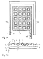
- FIGS. 1A to 1D An example of a structure of the prior art will be described in relation to FIGS. 1A to 1D, in which FIGS. 1A and 1B represent a top view of an electrode structure adopted in the case where there are two metallization levels for ensuring the connections of grids, sources and drains, FIGS. 1C and 1D representing corresponding cross-section views.
- DMOS type transistors that is to say Diffused MOS, with N channel, comprising source regions 1, layers 2 in which must be formed the channels, and regions of drains 3.
- This structure is formed in an epitaxial layer 4 of type N below which is a buried zone 5 of type N+ formed on a substrate 6 of type P. Conduction is done, when a bias is applied to gate electrodes 7 resting on a gate oxide layer 8, from the source regions 1 through the channel regions to the buried layer 5 of type N+ then going up towards the drain zones 3.
- deep diffusions of the N+ 9 type ensure better conduction between the drain zones 3 and the buried layer 5.
- This structure is only shown as an example of many structures of power MOS transistors that can be used.
- a gate electrode 7 illustrated in FIG. 1A is formed in a first connection level.
- an insulating layer is deposited on this conductive layer, for example a layer of SiO2, which is open at the locations represented in FIG. 1A by squares on the source regions inside the meshes of the grid electrode, by elongated fingers 11 on drain regions and through localized openings 7-1 at the periphery of the gate electrode 7.
- FIG. 1B shows a second interconnection level where we see the two interconnection levels and where the same layers as in the other figures are designated by the same references.
- an object of the present invention is to provide a new three-level interconnection structure for power MOS transistors in parallel allowing a general reduction in the resistance of access to the gates, sources and drains and obtaining a symmetrical source / drain structure.
- Another object of the present invention is to provide a new power MOS transistor structure particularly suited to the connection mode produced according to the first object of the invention.
- Another object of the present invention is to provide structures of MOS transistors with P and N channel, respectively, adapted to the connection mode according to the invention and compatible with each other.
- the present invention provides a structure of power MOS transistors in parallel, each of which comprises, on the same face of a substrate, gate, source and drain regions and three levels of connection layers, a first level of connection layer establishing contact with all the grids and a connection between each grid and the adjacent grids, this first level of connection layer comprising openings above the source and drain contact zones; this structure also comprises a first insulation layer open above the source and drain contact zones, a second level of connection layer establishing contact with all the source or drain zones and a connection between each zone of source (or drain) and the adjacent source (or drain) zones, openings isolating each drain (or source) contact, a second insulation layer open above the drain (or source) zones, a third level of continuous connection layer establishing contact with all the drain (or source) areas of the second level of connection layer.
- the first level of connection layer comprises polycrystalline silicon and a silicide and the second and third levels of connection layers comprise metallizations.
- complementary MOS transistor structures are provided, each of which consists of a transistor structure as stated above and in which, on the MOS of a first type, the second layer connection is associated with sources and, on MOS of the second type, the second connection layer is associated with drains.
- a structure of complementary field effect transistors particularly suitable for the present invention comprises a lateral N-channel transistor of DMOS type and a lateral P-channel transistor of extended drain type, in which, in N DMOS, the channel zone is separated from the drain area by a field oxide area and, in P MOS, the drain extension is formed under a field oxide area.
- the doping of the drain extension zone of the P MOS results from an implantation carried out in a self-aligned manner before the growth of the field oxide.
- FIGS. 2A, 2B and 2C will be better understood later on reading the description of examples of MOS transistors adapted to the present invention. Nevertheless, it suffices at first to conceive that one has produced in a semiconductor substrate MOS transistors in parallel, each of which comprises side by side a drain zone and a source zone of substantially the same surfaces separated by a grid zone. .
- MOS transistors in parallel, each of which comprises side by side a drain zone and a source zone of substantially the same surfaces separated by a grid zone.
- the drain and source zones are alternated like the black and white boxes of a chessboard, the grid zones corresponding to the limits between these boxes of the chessboard but obviously having a non-zero width.
- FIG. 2A represents a first level of metallization 20 in which only the gate electrode has been produced to establish a structure simply having the form of a grid. Openings are made in the gate electrode, these openings making it possible to see alternately a drain zone and a source zone.
- This first metallization level 20 is then covered with an insulating layer which is itself even open inside the boxes surrounded by the grid areas.
- this first level of connection may be a layer of polycrystalline silicon possibly covered with a layer of metallic silicide or partially or totally transformed into a metallic silicide or even be a refractory metal.
- FIG. 2B represents a second level of metallization which comes into contact with the exposed surfaces of the source and drain zones. Then, this metallization layer is etched as shown in the figure to leave in place: a source metallization 22 coming into contact with all the exposed source surfaces and ensuring a connection with each adjacent source metallization; - drain metallizations 23 coming into contact with each drain surface discovered but isolated from source metallizations and from other drain metallizations; - A metallization 24 coming into contact with the gate metallization of the first level shown in FIG. 2A and previously discovered at the appropriate location.
- an insulation layer is uniformly deposited on the surface of the wafer as shown in Figure 2B. Openings are formed at each of the drain metallizations 23 and at the output connections of the gate and source electrodes; and a third level of uniform metallization 25 as illustrated in FIG. 2C is deposited to interconnect all the drains and to ensure the output of the gate and source electrodes.
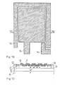
- FIG. 3 represents a sectional view of a portion of a group of N-type and parallel MOS transistors particularly suitable for an application according to the present invention.
- the metallizations are designated by the same references as in FIG. 2.
- This structure comprises a P-type substrate 30, a buried layer 31 of type N+ common to the entire structure of N-type MOS transistors in parallel but isolated from the corresponding buried layers of other MOS transistors existing on the same wafer, and an N-type epitaxial layer 32.
- the MOS transistors comprise channel 33, source 34 and drain 35 regions.
- the channel region 33 and the source region 34 being two successively diffused zones in the epitaxial layer 32, this structure is referred to as broadcast channel MOS or DMOS.
- FIG. 3 has the following specific features compared to a DMOS structure of conventional power: Field oxide zones 40 separate the channel zone proper below the grids 20 from the drain zones proper 35, that is to say that the drain comprises on the one hand the region 35 highly doped, on the other hand a region 41 located under said field oxide zones, of the same N-type doping but at a lower concentration.
- the region 41 can result from an implantation carried out before growth of the field oxide zones 40 and can therefore be self-aligned with these field oxide zones using the same mask as that which will serve to delimit the oxide zones of field.
- the region 33 commonly called channel region because it is in a surface part of this region disposed under the grid 20 that the channel is formed, has a particular structure.
- the gate electrode 20 includes a diffusion zone P delimited ted by the edge of the openings etched in the gate electrode 20, on the other hand, centrally, a region 45 of P+ type is provided which goes up to the surface of the substrate so that the source electrode 22 establishes contact on the one hand with the source region 34, on the other hand with this P+ type region 45. This produces a source-channel short circuit.
- FIG. 4 shows a sectional view of a portion of a group of P-channel MOS transistors particularly suitable for the arrangement of electrodes according to the present invention and also compatible from the point of view of its manufacture with the transistor structure N-channel DMOS described above.
- each transistor comprises channel zones 53, source 54 and drain 55.
- This transistor is of the composite channel type, also called extended drain. It has the following specificities: the drain zone 55 of the P+ type is surrounded by a field oxide mesh 60 under which extend 61 of the drain zone, also of the P type but more weakly doped than the drain zone of the type P+ proper. These extensions of the drain are designated by the reference 61. - As in the case of the structure in FIG. 3, it will be noted that these drain extension zones 61 under the field oxide zones 60 can be formed in self-alignment with the field oxide meshes 60 by providing an implantation delimited by the same mask as that which serves to delimit the fields oxide fields.
- the various metallization levels are designated by numerical references identical to those of FIGS. 2 and 3.
- the second level of metallization 22, 23 which, in FIG. 3, corresponds to the metallizations of sources and to the contact points of drains respectively, corresponds in FIG. 4, to the metallization of drains and to the contact points of sources.
- the third metallization level 25 which, in FIG. 3, is a drain metallization corresponds, in FIG. 4, to a source metallization.
- the main steps are:
- isolation foundations A boron implantation with a dose of 4X10¹⁴ Acm ⁇ 2 with an energy of 180 keV can be used. These P fond type isolation foundations (not shown) are intended, in conjunction with P diffusions Descending to isolate boxes in which logical MOS structures can be formed.
- drains are produced by diffusion from a phosphorus source, the P type zones by implantation of boron (1013 Acm ⁇ 2), the diffusion treatment can be carried out simultaneously at high temperature (1220 ° C for example for 4 to 6 hours).
- MOS transistors The realization of the MOS transistors is of the type of field oxidation localized by nitride, and with self-aligned field implantation, the field implantations are carried out with boron at 1013 Acm ⁇ 2 for P fields and arsenic 5X10¹² Acm ⁇ 2 for N fields. These implantations are carried out in regions which will be oxidized later to form regions of thick SiO2 thermal oxide (approximately 1 micrometer), regions not covered by nitride.
- These implantation regions will form either the field regions of a logical CMOS part, or the composite channels, or drain extensions (61) of the MOS transistors such as that represented in FIG. 4. This use for multiple purposes of field implantations constitutes an aspect of the present invention.
- the nitride protecting the active regions is then removed, the gate oxidation carried out, over a thickness of 50 to 100 nm, and the polycrystalline silicon layer 20 deposited and doped to form the first connection level.
- the etching of the gate electrodes of the different types of MOS transistors is then carried out simultaneously. Successive selections allow doping by implantation: channel 33 of DMOS with boron (2 to 6X10¹³ Acm ⁇ 2); the P+, drain 55 and source 54, P MOS and short-circuit 45 regions of the DMOS with boron (5 to 8 ⁇ 1014 Acm ⁇ 2); and finally the N+ regions forming the drains and sources of DMOS (to do this, a dose of arsenic from 5 to 7X10¹⁵ Acm ⁇ 2 can be used). These different layouts are followed by appropriate heat treatments so as to restore the defects and obtain the optimum junction depths. Typical depths of 1 to 1.5 micrometers for the N+ and P+ regions allow efficient power transistors to be obtained.
- the doping of the active regions occurring after the etching of the gate electrodes in the polycrystalline silicon layer it is possible to align the different regions on the edge of these electrodes.
- aligning the drain extension under the thick oxide eliminates positioning differences and reduces the size of the drain extension to the value required to laterally support the necessary tension.
- the metallizations of the second and third connection levels can be carried out by the following successive operations: - depositing an insulating layer on the gate electrode 20; - Etching of openings in this layer exposing the silicon; - deposit of a metal layer and etching of the interconnections.
- a source electrode 22 formed of a mesh network and isolated pads 23 will be obtained on the drains of each elementary MOS; depositing an insulating layer and opening passages at the level of the pellets 23 previously reserved on each drain.
- This operation may require several successive deposits and attacks by dry etching, so as to obtain a sufficiently flat insulation layer to allow proper isolation and crossing of the second metal layer; - deposition of the second metal layer and etching of the drain electrodes 25.
- the metal electrodes are etched in aluminum layers doped with silicon and copper and the dielectric layers obtained by chemical vapor deposition of SiO2 (CVD) doped with phosphorus.
- SiO2 chemical vapor deposition of SiO2 (CVD) doped with phosphorus.
- TiW-Al composite layers with silicide (Pt-Si) contacts have also been used with success.
- the main characteristics of the electrodes are as follows: - They form in three separate planes a mesh network of interconnections of the gate, source and drain regions of the different elementary cells; each interconnection plane is isolated from the next by a dielectric layer, the thickness of which can be adjusted as a function of the characteristics sought.
- This configuration gives the assembly of the elementary cells the following interesting electrical properties: - obtaining the minimum resistance between the equivalent electrodes, grid, drain or source, of two cells elementary whatever their arrangement in the ribbon constituting the power transistor; - coverage of the total surface of the device by all of the electrodes: this arrangement allows the drain and source electrodes to play the role of electrostatic screen. It is particularly interesting in the case of MOS transistors with extended drain to ensure the stability and the minimum field at the surface of the transistor; the search for the optimum screen effect implies in the case represented in FIG.
- the source electrodes will be connected at level 2 and those of drain at level 3 in the case of an N-channel DMOS, whereas the reverse order will be adopted in the case of the P-channel MOS, the drain being this time connected at level 2 and the source at level 3.
- the polycrystalline silicon gate electrode is produced first and constitutes level 1; it can be connected either with level 2 or with level 3, the pads necessary for soldering the connections to the housing being always made in the last metallization layer; -
- This particular arrangement of multi-layer electrodes allows, by adjusting the thicknesses of the dielectrics which isolate them, to obtain a gradual field screen effect and maximum voltage withstand of the MOS transistors of the two types.
Landscapes
- Insulated Gate Type Field-Effect Transistor (AREA)
- Metal-Oxide And Bipolar Metal-Oxide Semiconductor Integrated Circuits (AREA)
- Internal Circuitry In Semiconductor Integrated Circuit Devices (AREA)
Applications Claiming Priority (2)
| Application Number | Priority Date | Filing Date | Title |
|---|---|---|---|
| FR8709157 | 1987-06-22 | ||
| FR8709157A FR2616966B1 (fr) | 1987-06-22 | 1987-06-22 | Structure de transistors mos de puissance |
Publications (2)
| Publication Number | Publication Date |
|---|---|
| EP0296997A1 true EP0296997A1 (de) | 1988-12-28 |
| EP0296997B1 EP0296997B1 (de) | 1992-08-19 |
Family
ID=9352634
Family Applications (1)
| Application Number | Title | Priority Date | Filing Date |
|---|---|---|---|
| EP88420206A Expired - Lifetime EP0296997B1 (de) | 1987-06-22 | 1988-06-21 | MOS-Leistungstransistoranordnung |
Country Status (6)
| Country | Link |
|---|---|
| US (1) | US4890142A (de) |
| EP (1) | EP0296997B1 (de) |
| JP (1) | JP2842871B2 (de) |
| KR (1) | KR890001200A (de) |
| DE (1) | DE3873839T2 (de) |
| FR (1) | FR2616966B1 (de) |
Cited By (7)
| Publication number | Priority date | Publication date | Assignee | Title |
|---|---|---|---|---|
| EP0550015A1 (de) * | 1991-12-30 | 1993-07-07 | Texas Instruments Incorporated | Lateraler zweifach diffundierter Fieldeffekttransistor mit einem isolierten Gate und Verfahren zur Herstellung |
| WO1995024055A1 (de) * | 1994-03-04 | 1995-09-08 | Siemens Aktiengesellschaft | Mis-struktur auf siliciumcarbid-basis mit hoher latch-up-festigkeit |
| US5464992A (en) * | 1990-06-08 | 1995-11-07 | Nippondenso Co., Ltd. | Insulated gate bipolar transistor provided with a minority carrier extracting layer |
| EP0714128A3 (de) * | 1994-11-02 | 1996-07-17 | Texas Instruments Inc | Verbesserungen in oder in Beziehung auf integrierte Schaltungen |
| EP0805499A3 (de) * | 1992-08-17 | 1997-11-26 | Fuji Electric Co., Ltd. | MIS-Feldeffekttransistor mit hoher Spannungsfestigkeit und integrierte Halbleiterschaltung |
| US6140702A (en) * | 1996-05-31 | 2000-10-31 | Texas Instruments Incorporated | Plastic encapsulation for integrated circuits having plated copper top surface level interconnect |
| US6140150A (en) * | 1997-05-28 | 2000-10-31 | Texas Instruments Incorporated | Plastic encapsulation for integrated circuits having plated copper top surface level interconnect |
Families Citing this family (24)
| Publication number | Priority date | Publication date | Assignee | Title |
|---|---|---|---|---|
| US4998151A (en) * | 1989-04-13 | 1991-03-05 | General Electric Company | Power field effect devices having small cell size and low contact resistance |
| USRE37424E1 (en) * | 1989-06-14 | 2001-10-30 | Stmicroelectronics S.R.L. | Mixed technology integrated device comprising complementary LDMOS power transistors, CMOS and vertical PNP integrated structures having an enhanced ability to withstand a relatively high supply voltage |
| US5192989A (en) * | 1989-11-28 | 1993-03-09 | Nissan Motor Co., Ltd. | Lateral dmos fet device with reduced on resistance |
| IT1252625B (it) * | 1991-12-05 | 1995-06-19 | Cons Ric Microelettronica | Processo di fabbricazione di transistors a effetto di campo con gate isolato (igfet) a bassa densita' di corto circuiti tra gate e source e dispositivi con esso ottenuti |
| US5283454A (en) * | 1992-09-11 | 1994-02-01 | Motorola, Inc. | Semiconductor device including very low sheet resistivity buried layer |
| US5631177A (en) * | 1992-12-07 | 1997-05-20 | Sgs-Thomson Microelectronics, S.R.L. | Process for manufacturing integrated circuit with power field effect transistors |
| US5382536A (en) * | 1993-03-15 | 1995-01-17 | Texas Instruments Incorporated | Method of fabricating lateral DMOS structure |
| US5369045A (en) * | 1993-07-01 | 1994-11-29 | Texas Instruments Incorporated | Method for forming a self-aligned lateral DMOS transistor |
| US5798287A (en) * | 1993-12-24 | 1998-08-25 | Consorzio Per La Ricerca Sulla Microelettronica Nel Mezzogiorno | Method for forming a power MOS device chip |
| EP0660396B1 (de) * | 1993-12-24 | 1998-11-04 | Consorzio per la Ricerca sulla Microelettronica nel Mezzogiorno | MOS-Leistungs-Chip-Typ und Packungszusammenbau |
| DE69321966T2 (de) * | 1993-12-24 | 1999-06-02 | Consorzio Per La Ricerca Sulla Microelettronica Nel Mezzogiorno, Catania | Leistungs-Halbleiterbauelement |
| JP3136885B2 (ja) * | 1994-02-02 | 2001-02-19 | 日産自動車株式会社 | パワーmosfet |
| JP3355817B2 (ja) * | 1994-10-20 | 2002-12-09 | 株式会社デンソー | 半導体装置 |
| KR100468342B1 (ko) | 1996-05-15 | 2005-06-02 | 텍사스 인스트루먼츠 인코포레이티드 | 자기-정렬resurf영역을가진ldmos장치및그제조방법 |
| JP3327135B2 (ja) * | 1996-09-09 | 2002-09-24 | 日産自動車株式会社 | 電界効果トランジスタ |
| JP3395603B2 (ja) * | 1997-09-26 | 2003-04-14 | 株式会社豊田中央研究所 | 横型mos素子を含む半導体装置 |
| US6531355B2 (en) | 1999-01-25 | 2003-03-11 | Texas Instruments Incorporated | LDMOS device with self-aligned RESURF region and method of fabrication |
| DE10104274C5 (de) * | 2000-02-04 | 2008-05-29 | International Rectifier Corp., El Segundo | Halbleiterbauteil mit MOS-Gatesteuerung und mit einer Kontaktstruktur sowie Verfahren zu seiner Herstellung |
| US6653708B2 (en) | 2000-08-08 | 2003-11-25 | Intersil Americas Inc. | Complementary metal oxide semiconductor with improved single event performance |
| JP2004079988A (ja) * | 2002-06-19 | 2004-03-11 | Toshiba Corp | 半導体装置 |
| EP1915783A2 (de) * | 2005-08-10 | 2008-04-30 | Nxp B.V. | Ldmos-transistor |
| JP2007273689A (ja) * | 2006-03-31 | 2007-10-18 | Denso Corp | 半導体装置 |
| US8169081B1 (en) | 2007-12-27 | 2012-05-01 | Volterra Semiconductor Corporation | Conductive routings in integrated circuits using under bump metallization |
| US8084821B2 (en) * | 2008-01-30 | 2011-12-27 | Infineon Technologies Ag | Integrated circuit including a power MOS transistor |
Citations (5)
| Publication number | Priority date | Publication date | Assignee | Title |
|---|---|---|---|---|
| DE3046749A1 (de) * | 1979-12-10 | 1981-09-10 | Sharp K.K., Osaka | "mos-halbleiterbauelement fuer hohe betriebsspannungen" |
| GB2098799A (en) * | 1981-05-20 | 1982-11-24 | Nippon Electric Co | Multi-level interconnection system for integrated circuits |
| EP0132861A1 (de) * | 1983-06-13 | 1985-02-13 | Koninklijke Philips Electronics N.V. | Halbleiteranordnung mit einem Feldeffekttransistor |
| EP0179693A1 (de) * | 1984-09-28 | 1986-04-30 | Thomson-Csf | Integrierte Schaltungsstruktur mit CMOS-Transistoren für höhere Spannungen und Verfahren zu ihrer Herstellung |
| US4589004A (en) * | 1981-03-30 | 1986-05-13 | Tokyo Shibaura Denki Kabushiki Kaisha | Semiconductor device monolithically comprising a V-MOSFET and bipolar transistor isolated from each other |
Family Cites Families (4)
| Publication number | Priority date | Publication date | Assignee | Title |
|---|---|---|---|---|
| JPS5193878A (de) * | 1975-02-17 | 1976-08-17 | ||
| JPS57194567A (en) * | 1981-05-27 | 1982-11-30 | Hitachi Ltd | Semiconductor memory device |
| JPS58171861A (ja) * | 1982-04-01 | 1983-10-08 | Toshiba Corp | 半導体装置 |
| JPS604253A (ja) * | 1983-06-23 | 1985-01-10 | Nec Corp | 半導体集積回路メモリ |
-
1987
- 1987-06-22 FR FR8709157A patent/FR2616966B1/fr not_active Expired
-
1988
- 1988-06-16 KR KR1019880007239A patent/KR890001200A/ko not_active Withdrawn
- 1988-06-17 US US07/208,224 patent/US4890142A/en not_active Expired - Lifetime
- 1988-06-20 JP JP63152107A patent/JP2842871B2/ja not_active Expired - Lifetime
- 1988-06-21 DE DE8888420206T patent/DE3873839T2/de not_active Expired - Lifetime
- 1988-06-21 EP EP88420206A patent/EP0296997B1/de not_active Expired - Lifetime
Patent Citations (5)
| Publication number | Priority date | Publication date | Assignee | Title |
|---|---|---|---|---|
| DE3046749A1 (de) * | 1979-12-10 | 1981-09-10 | Sharp K.K., Osaka | "mos-halbleiterbauelement fuer hohe betriebsspannungen" |
| US4589004A (en) * | 1981-03-30 | 1986-05-13 | Tokyo Shibaura Denki Kabushiki Kaisha | Semiconductor device monolithically comprising a V-MOSFET and bipolar transistor isolated from each other |
| GB2098799A (en) * | 1981-05-20 | 1982-11-24 | Nippon Electric Co | Multi-level interconnection system for integrated circuits |
| EP0132861A1 (de) * | 1983-06-13 | 1985-02-13 | Koninklijke Philips Electronics N.V. | Halbleiteranordnung mit einem Feldeffekttransistor |
| EP0179693A1 (de) * | 1984-09-28 | 1986-04-30 | Thomson-Csf | Integrierte Schaltungsstruktur mit CMOS-Transistoren für höhere Spannungen und Verfahren zu ihrer Herstellung |
Cited By (7)
| Publication number | Priority date | Publication date | Assignee | Title |
|---|---|---|---|---|
| US5464992A (en) * | 1990-06-08 | 1995-11-07 | Nippondenso Co., Ltd. | Insulated gate bipolar transistor provided with a minority carrier extracting layer |
| EP0550015A1 (de) * | 1991-12-30 | 1993-07-07 | Texas Instruments Incorporated | Lateraler zweifach diffundierter Fieldeffekttransistor mit einem isolierten Gate und Verfahren zur Herstellung |
| EP0805499A3 (de) * | 1992-08-17 | 1997-11-26 | Fuji Electric Co., Ltd. | MIS-Feldeffekttransistor mit hoher Spannungsfestigkeit und integrierte Halbleiterschaltung |
| WO1995024055A1 (de) * | 1994-03-04 | 1995-09-08 | Siemens Aktiengesellschaft | Mis-struktur auf siliciumcarbid-basis mit hoher latch-up-festigkeit |
| EP0714128A3 (de) * | 1994-11-02 | 1996-07-17 | Texas Instruments Inc | Verbesserungen in oder in Beziehung auf integrierte Schaltungen |
| US6140702A (en) * | 1996-05-31 | 2000-10-31 | Texas Instruments Incorporated | Plastic encapsulation for integrated circuits having plated copper top surface level interconnect |
| US6140150A (en) * | 1997-05-28 | 2000-10-31 | Texas Instruments Incorporated | Plastic encapsulation for integrated circuits having plated copper top surface level interconnect |
Also Published As
| Publication number | Publication date |
|---|---|
| DE3873839D1 (de) | 1992-09-24 |
| KR890001200A (ko) | 1989-03-18 |
| JPS6420666A (en) | 1989-01-24 |
| EP0296997B1 (de) | 1992-08-19 |
| US4890142A (en) | 1989-12-26 |
| JP2842871B2 (ja) | 1999-01-06 |
| FR2616966B1 (fr) | 1989-10-27 |
| FR2616966A1 (fr) | 1988-12-23 |
| DE3873839T2 (de) | 1993-05-13 |
Similar Documents
| Publication | Publication Date | Title |
|---|---|---|
| EP0296997B1 (de) | MOS-Leistungstransistoranordnung | |
| EP0810665B1 (de) | Kompakte ROM-Speichermatrix | |
| EP0258141B1 (de) | MIS integrierte Schaltung, wie eine EPROM-Speicherzelle, und Verfahren zu deren Herstellung | |
| FR2776837A1 (fr) | Architecture de bus a transistor mosfet de puissance a couplage de champ, utilisant la technologie a tranchees | |
| EP0057126B1 (de) | Verfahren zur Herstellung einer Transistorstruktur | |
| FR2738079A1 (fr) | Dispositif a semiconducteurs, a tranchee, et procede de fabrication | |
| EP0017697A1 (de) | Verbindungsvorrichtung für integrierte Halbleiterschaltungen und Verfahren zu ihrer Herstellung | |
| FR2499749A1 (fr) | Dispositif de memoire a semiconducteurs et procede de fabrication d'un tel dispositif | |
| EP0022388B1 (de) | Verfahren zur Herstellung eines vertikalen Feldeffekttransistors vom DMOS-Typ | |
| EP0461967A2 (de) | Halbleiteranordnung mit Schottky-Übergang für Mikrowellenverstärkung und schnelle logische Schaltungen und Verfahren zu deren Herstellung | |
| EP0843355A1 (de) | Herstellung von integrierten Bipolar-/CMOS-Schaltkreisen und einem Kondensator | |
| EP1675184A1 (de) | Schottkydiode mit vertikaler Barriere | |
| KR100397517B1 (ko) | 고체 촬상장치 및 그 제조방법 | |
| FR2484142A1 (fr) | Dispositif en circuit integre | |
| Brown et al. | Transparent metal oxide electrode CID imager | |
| EP0157677B2 (de) | Verfahren zur Verbindung der aktiven Bereiche und/oder der Steuerelektroden von einer CMOS-integrierten Schaltung | |
| EP1006573A1 (de) | Herstellungsverfahren für integrierte BiCMOS Schaltkreise auf einem gewöhnlichen CMOS Substrat | |
| FR2511539A1 (fr) | Dispositif de memoire remanente | |
| FR2787637A1 (fr) | Structure peripherique pour dispositif monolithique de puissance | |
| FR2894069A1 (fr) | Fabrication de transistors mos | |
| EP0019560B1 (de) | Torschaltungen aus MOS-Transistoren mit mehrfachen Drains | |
| FR3079965A1 (fr) | Circuit integre a transistors a base commune | |
| FR2607966A1 (fr) | Arrangement de circuits a semi-conducteur avec interconnexion d'ilots semiconducteurs sur substrat isolant, et son procede de fabrication | |
| EP0170571B1 (de) | CMOS-statische Speicherzelle | |
| EP0186720B1 (de) | Vordiffundierte Mehrfunktionstechnik in CMOS-Technik |
Legal Events
| Date | Code | Title | Description |
|---|---|---|---|
| PUAI | Public reference made under article 153(3) epc to a published international application that has entered the european phase |
Free format text: ORIGINAL CODE: 0009012 |
|
| AK | Designated contracting states |
Kind code of ref document: A1 Designated state(s): BE DE FR GB IT NL |
|
| 17P | Request for examination filed |
Effective date: 19890614 |
|
| 17Q | First examination report despatched |
Effective date: 19910930 |
|
| GRAA | (expected) grant |
Free format text: ORIGINAL CODE: 0009210 |
|
| AK | Designated contracting states |
Kind code of ref document: B1 Designated state(s): BE DE FR GB IT NL |
|
| PG25 | Lapsed in a contracting state [announced via postgrant information from national office to epo] |
Ref country code: NL Effective date: 19920819 |
|
| ITF | It: translation for a ep patent filed | ||
| REF | Corresponds to: |
Ref document number: 3873839 Country of ref document: DE Date of ref document: 19920924 |
|
| GBT | Gb: translation of ep patent filed (gb section 77(6)(a)/1977) | ||
| NLV1 | Nl: lapsed or annulled due to failure to fulfill the requirements of art. 29p and 29m of the patents act | ||
| PLBE | No opposition filed within time limit |
Free format text: ORIGINAL CODE: 0009261 |
|
| STAA | Information on the status of an ep patent application or granted ep patent |
Free format text: STATUS: NO OPPOSITION FILED WITHIN TIME LIMIT |
|
| PG25 | Lapsed in a contracting state [announced via postgrant information from national office to epo] |
Ref country code: BE Effective date: 19930630 |
|
| 26N | No opposition filed | ||
| BERE | Be: lapsed |
Owner name: S.A. SGS-THOMSON MICROELECTRONICS Effective date: 19930630 |
|
| REG | Reference to a national code |
Ref country code: FR Ref legal event code: D6 |
|
| REG | Reference to a national code |
Ref country code: GB Ref legal event code: IF02 |
|
| PGFP | Annual fee paid to national office [announced via postgrant information from national office to epo] |
Ref country code: DE Payment date: 20070530 Year of fee payment: 20 |
|
| PGFP | Annual fee paid to national office [announced via postgrant information from national office to epo] |
Ref country code: GB Payment date: 20070530 Year of fee payment: 20 |
|
| PGFP | Annual fee paid to national office [announced via postgrant information from national office to epo] |
Ref country code: IT Payment date: 20070620 Year of fee payment: 20 |
|
| PGFP | Annual fee paid to national office [announced via postgrant information from national office to epo] |
Ref country code: FR Payment date: 20070627 Year of fee payment: 20 |
|
| REG | Reference to a national code |
Ref country code: GB Ref legal event code: PE20 Expiry date: 20080620 |
|
| PG25 | Lapsed in a contracting state [announced via postgrant information from national office to epo] |
Ref country code: GB Free format text: LAPSE BECAUSE OF EXPIRATION OF PROTECTION Effective date: 20080620 |