EP0017697A1 - Verbindungsvorrichtung für integrierte Halbleiterschaltungen und Verfahren zu ihrer Herstellung - Google Patents
Verbindungsvorrichtung für integrierte Halbleiterschaltungen und Verfahren zu ihrer Herstellung Download PDFInfo
- Publication number
- EP0017697A1 EP0017697A1 EP80100189A EP80100189A EP0017697A1 EP 0017697 A1 EP0017697 A1 EP 0017697A1 EP 80100189 A EP80100189 A EP 80100189A EP 80100189 A EP80100189 A EP 80100189A EP 0017697 A1 EP0017697 A1 EP 0017697A1
- Authority
- EP
- European Patent Office
- Prior art keywords
- region
- layer
- oxide
- semiconductor
- door
- Prior art date
- Legal status (The legal status is an assumption and is not a legal conclusion. Google has not performed a legal analysis and makes no representation as to the accuracy of the status listed.)
- Granted
Links
Images


Classifications
-
- H—ELECTRICITY
- H10—SEMICONDUCTOR DEVICES; ELECTRIC SOLID-STATE DEVICES NOT OTHERWISE PROVIDED FOR
- H10B—ELECTRONIC MEMORY DEVICES
- H10B12/00—Dynamic random access memory [DRAM] devices
- H10B12/30—DRAM devices comprising one-transistor - one-capacitor [1T-1C] memory cells
-
- H—ELECTRICITY
- H10—SEMICONDUCTOR DEVICES; ELECTRIC SOLID-STATE DEVICES NOT OTHERWISE PROVIDED FOR
- H10D—INORGANIC ELECTRIC SEMICONDUCTOR DEVICES
- H10D64/00—Electrodes of devices having potential barriers
- H10D64/60—Electrodes characterised by their materials
- H10D64/66—Electrodes having a conductor capacitively coupled to a semiconductor by an insulator, e.g. MIS electrodes
- H10D64/671—Electrodes having a conductor capacitively coupled to a semiconductor by an insulator, e.g. MIS electrodes the conductor having lateral variation in doping or structure
-
- H—ELECTRICITY
- H10—SEMICONDUCTOR DEVICES; ELECTRIC SOLID-STATE DEVICES NOT OTHERWISE PROVIDED FOR
- H10D—INORGANIC ELECTRIC SEMICONDUCTOR DEVICES
- H10D30/00—Field-effect transistors [FET]
- H10D30/01—Manufacture or treatment
- H10D30/021—Manufacture or treatment of FETs having insulated gates [IGFET]
- H10D30/0223—Manufacture or treatment of FETs having insulated gates [IGFET] having source and drain regions or source and drain extensions self-aligned to sides of the gate
-
- H—ELECTRICITY
- H10—SEMICONDUCTOR DEVICES; ELECTRIC SOLID-STATE DEVICES NOT OTHERWISE PROVIDED FOR
- H10D—INORGANIC ELECTRIC SEMICONDUCTOR DEVICES
- H10D30/00—Field-effect transistors [FET]
- H10D30/01—Manufacture or treatment
- H10D30/021—Manufacture or treatment of FETs having insulated gates [IGFET]
- H10D30/027—Manufacture or treatment of FETs having insulated gates [IGFET] of lateral single-gate IGFETs
- H10D30/0273—Manufacture or treatment of FETs having insulated gates [IGFET] of lateral single-gate IGFETs forming final gates or dummy gates after forming source and drain electrodes, e.g. contact first technology
-
- H—ELECTRICITY
- H10—SEMICONDUCTOR DEVICES; ELECTRIC SOLID-STATE DEVICES NOT OTHERWISE PROVIDED FOR
- H10D—INORGANIC ELECTRIC SEMICONDUCTOR DEVICES
- H10D64/00—Electrodes of devices having potential barriers
- H10D64/01—Manufacture or treatment
- H10D64/013—Manufacture or treatment of electrodes having a conductor capacitively coupled to a semiconductor by an insulator
- H10D64/01302—Manufacture or treatment of electrodes having a conductor capacitively coupled to a semiconductor by an insulator the insulator being formed after the semiconductor body, the semiconductor being silicon
- H10D64/01304—Manufacture or treatment of electrodes having a conductor capacitively coupled to a semiconductor by an insulator the insulator being formed after the semiconductor body, the semiconductor being silicon characterised by the conductor
- H10D64/01306—Manufacture or treatment of electrodes having a conductor capacitively coupled to a semiconductor by an insulator the insulator being formed after the semiconductor body, the semiconductor being silicon characterised by the conductor the conductor comprising a layer of silicon contacting the insulator, e.g. polysilicon
- H10D64/01308—Manufacture or treatment of electrodes having a conductor capacitively coupled to a semiconductor by an insulator the insulator being formed after the semiconductor body, the semiconductor being silicon characterised by the conductor the conductor comprising a layer of silicon contacting the insulator, e.g. polysilicon the conductor further comprising a non-elemental silicon additional conductive layer, e.g. a metal silicide layer formed by the reaction of silicon with an implanted metal
- H10D64/01312—Manufacture or treatment of electrodes having a conductor capacitively coupled to a semiconductor by an insulator the insulator being formed after the semiconductor body, the semiconductor being silicon characterised by the conductor the conductor comprising a layer of silicon contacting the insulator, e.g. polysilicon the conductor further comprising a non-elemental silicon additional conductive layer, e.g. a metal silicide layer formed by the reaction of silicon with an implanted metal the additional layer comprising a metal or metal silicide formed by deposition, i.e. without a silicidation reaction, e.g. sputter deposition
-
- H—ELECTRICITY
- H10—SEMICONDUCTOR DEVICES; ELECTRIC SOLID-STATE DEVICES NOT OTHERWISE PROVIDED FOR
- H10D—INORGANIC ELECTRIC SEMICONDUCTOR DEVICES
- H10D64/00—Electrodes of devices having potential barriers
- H10D64/60—Electrodes characterised by their materials
- H10D64/66—Electrodes having a conductor capacitively coupled to a semiconductor by an insulator, e.g. MIS electrodes
- H10D64/661—Electrodes having a conductor capacitively coupled to a semiconductor by an insulator, e.g. MIS electrodes the conductor comprising a layer of silicon contacting the insulator, e.g. polysilicon having vertical doping variation
- H10D64/662—Electrodes having a conductor capacitively coupled to a semiconductor by an insulator, e.g. MIS electrodes the conductor comprising a layer of silicon contacting the insulator, e.g. polysilicon having vertical doping variation the conductor further comprising additional layers, e.g. multiple silicon layers having different crystal structures
- H10D64/663—Electrodes having a conductor capacitively coupled to a semiconductor by an insulator, e.g. MIS electrodes the conductor comprising a layer of silicon contacting the insulator, e.g. polysilicon having vertical doping variation the conductor further comprising additional layers, e.g. multiple silicon layers having different crystal structures the additional layers comprising a silicide layer contacting the layer of silicon, e.g. polycide gates
-
- H—ELECTRICITY
- H10—SEMICONDUCTOR DEVICES; ELECTRIC SOLID-STATE DEVICES NOT OTHERWISE PROVIDED FOR
- H10W—GENERIC PACKAGES, INTERCONNECTIONS, CONNECTORS OR OTHER CONSTRUCTIONAL DETAILS OF DEVICES COVERED BY CLASS H10
- H10W20/00—Interconnections in chips, wafers or substrates
- H10W20/40—Interconnections external to wafers or substrates, e.g. back-end-of-line [BEOL] metallisations or vias connecting to gate electrodes
- H10W20/41—Interconnections external to wafers or substrates, e.g. back-end-of-line [BEOL] metallisations or vias connecting to gate electrodes characterised by their conductive parts
- H10W20/44—Conductive materials thereof
- H10W20/4451—Semiconductor materials, e.g. polysilicon
-
- H—ELECTRICITY
- H10—SEMICONDUCTOR DEVICES; ELECTRIC SOLID-STATE DEVICES NOT OTHERWISE PROVIDED FOR
- H10W—GENERIC PACKAGES, INTERCONNECTIONS, CONNECTORS OR OTHER CONSTRUCTIONAL DETAILS OF DEVICES COVERED BY CLASS H10
- H10W20/00—Interconnections in chips, wafers or substrates
- H10W20/40—Interconnections external to wafers or substrates, e.g. back-end-of-line [BEOL] metallisations or vias connecting to gate electrodes
- H10W20/495—Capacitive arrangements or effects of, or between wiring layers
-
- H—ELECTRICITY
- H10—SEMICONDUCTOR DEVICES; ELECTRIC SOLID-STATE DEVICES NOT OTHERWISE PROVIDED FOR
- H10W—GENERIC PACKAGES, INTERCONNECTIONS, CONNECTORS OR OTHER CONSTRUCTIONAL DETAILS OF DEVICES COVERED BY CLASS H10
- H10W74/00—Encapsulations, e.g. protective coatings
- H10W74/10—Encapsulations, e.g. protective coatings characterised by their shape or disposition
- H10W74/131—Encapsulations, e.g. protective coatings characterised by their shape or disposition the semiconductor body being only partially enclosed
- H10W74/137—Encapsulations, e.g. protective coatings characterised by their shape or disposition the semiconductor body being only partially enclosed the encapsulations being directly on the semiconductor body
-
- H—ELECTRICITY
- H10—SEMICONDUCTOR DEVICES; ELECTRIC SOLID-STATE DEVICES NOT OTHERWISE PROVIDED FOR
- H10W—GENERIC PACKAGES, INTERCONNECTIONS, CONNECTORS OR OTHER CONSTRUCTIONAL DETAILS OF DEVICES COVERED BY CLASS H10
- H10W74/00—Encapsulations, e.g. protective coatings
- H10W74/40—Encapsulations, e.g. protective coatings characterised by their materials
- H10W74/43—Encapsulations, e.g. protective coatings characterised by their materials comprising oxides, nitrides or carbides, e.g. ceramics or glasses
Definitions
- integrated circuit structures contain several devices made from a semiconductor crystal and comprise multi-level interconnection lines arranged above the devices and above the insulating regions. of the structure.
- the interconnection lines have been formed in various ways in the prior art, for example by gas diffusion, by doping with ion implantation and by the use of doped polycrystalline semiconductor material.
- reducing the dimensions of the integrated devices causes the resistance to increase to levels seriously affecting the performance of these devices.
- the delay due to the interconnections of the integrated devices constitutes a large and unacceptable part of the total delay due to the circuits themselves.
- the voltage drops become greater, making it more difficult to distribute power and detect signals.
- the present invention relates to a technique for manufacturing integrated circuits in which the interconnections are formed from conductive lines composed of doped polycrystalline silicon and metallic silicide.
- This combination which will hereinafter be called “polyciure”, makes it possible to simultaneously obtain the advantage of a high conductivity and that of a reduced stray capacitance.
- the most suitable metals are those which form passivation and isolation oxides with silicon, such as tungsten, molybdenum, tantalum, titanium and rhodium.
- a layer of silicon dioxide 5 is then formed on the layer 3.
- the layer 5 can be either formed on site, or obtained partially by growth and then partially by deposit, or even obtained only by deposit.
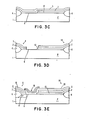
- Figure 3B shows the next step in which part of the oxide layer 12 is etched, which exposes part of the surface of the crystal 1, and the layer of photoresist 13 is removed.
Landscapes
- Internal Circuitry In Semiconductor Integrated Circuit Devices (AREA)
- Semiconductor Memories (AREA)
- Electrodes Of Semiconductors (AREA)
- Bipolar Transistors (AREA)
Applications Claiming Priority (2)
| Application Number | Priority Date | Filing Date | Title |
|---|---|---|---|
| US06/016,647 US4329706A (en) | 1979-03-01 | 1979-03-01 | Doped polysilicon silicide semiconductor integrated circuit interconnections |
| US16647 | 1979-03-01 |
Publications (2)
| Publication Number | Publication Date |
|---|---|
| EP0017697A1 true EP0017697A1 (de) | 1980-10-29 |
| EP0017697B1 EP0017697B1 (de) | 1984-05-02 |
Family
ID=21778214
Family Applications (1)
| Application Number | Title | Priority Date | Filing Date |
|---|---|---|---|
| EP80100189A Expired EP0017697B1 (de) | 1979-03-01 | 1980-01-16 | Verbindungsvorrichtung für integrierte Halbleiterschaltungen und Verfahren zu ihrer Herstellung |
Country Status (4)
| Country | Link |
|---|---|
| US (1) | US4329706A (de) |
| EP (1) | EP0017697B1 (de) |
| JP (1) | JPS55118651A (de) |
| DE (1) | DE3067661D1 (de) |
Cited By (5)
| Publication number | Priority date | Publication date | Assignee | Title |
|---|---|---|---|---|
| EP0070751A1 (de) * | 1981-07-13 | 1983-01-26 | FAIRCHILD CAMERA & INSTRUMENT CORPORATION | Verfahren zum gleichzeitigen Aufdampfen von Metall und Silizium unter niedrigem Druck zur Bildung von Metallsilicid |
| EP0072522A3 (en) * | 1981-08-19 | 1983-11-09 | Siemens Aktiengesellschaft | Process for manufacturing integrated mos field effect transistors, particularly circuits having complementary mos field effect transistors with an additional conductor level comprising metal silicides |
| EP0075085A3 (en) * | 1981-09-21 | 1985-01-16 | International Business Machines Corporation | Method of fabricating a conductive metal silicide structure |
| EP0055161B1 (de) * | 1980-12-09 | 1985-09-04 | FAIRCHILD CAMERA & INSTRUMENT CORPORATION | Mehrschichtige Metallsilizid-Verbindungsleiter für integrierte Schaltungen |
| EP0096734B1 (de) * | 1982-05-31 | 1986-08-20 | Kabushiki Kaisha Toshiba | Inverter mit übereinanderliegendem komplementären Metall-Oxyd-Halbleiter |
Families Citing this family (95)
| Publication number | Priority date | Publication date | Assignee | Title |
|---|---|---|---|---|
| DE3069973D1 (en) * | 1979-08-25 | 1985-02-28 | Zaidan Hojin Handotai Kenkyu | Insulated-gate field-effect transistor |
| JPS5927102B2 (ja) * | 1979-12-24 | 1984-07-03 | 富士通株式会社 | 半導体記憶装置 |
| JPS56126969A (en) * | 1980-03-11 | 1981-10-05 | Toshiba Corp | Integrated circuit device |
| JPS56150851A (en) * | 1980-04-22 | 1981-11-21 | Toshiba Corp | Manufacture of semiconductor integrated circuit |
| US5109258A (en) * | 1980-05-07 | 1992-04-28 | Texas Instruments Incorporated | Memory cell made by selective oxidation of polysilicon |
| JPS5718356A (en) * | 1980-07-07 | 1982-01-30 | Mitsubishi Electric Corp | Semiconductor memory storage |
| JPS5737888A (en) * | 1980-08-19 | 1982-03-02 | Mitsubishi Electric Corp | Photo detector |
| EP0048610B1 (de) * | 1980-09-22 | 1986-01-15 | Kabushiki Kaisha Toshiba | Halbleiterbauelement und Verfahren zu seiner Herstellung |
| US4545113A (en) * | 1980-10-23 | 1985-10-08 | Fairchild Camera & Instrument Corporation | Process for fabricating a lateral transistor having self-aligned base and base contact |
| JPS5951128B2 (ja) * | 1980-11-07 | 1984-12-12 | 富士通株式会社 | 半導体装置 |
| US4445134A (en) * | 1980-12-08 | 1984-04-24 | Ibm Corporation | Conductivity WSi2 films by Pt preanneal layering |
| US4488166A (en) * | 1980-12-09 | 1984-12-11 | Fairchild Camera & Instrument Corp. | Multilayer metal silicide interconnections for integrated circuits |
| US4403394A (en) * | 1980-12-17 | 1983-09-13 | International Business Machines Corporation | Formation of bit lines for ram device |
| US4449224A (en) * | 1980-12-29 | 1984-05-15 | Eliyahou Harari | Dynamic merged load logic (MLL) and merged load memory (MLM) |
| JPS58500680A (ja) * | 1981-05-04 | 1983-04-28 | モトロ−ラ・インコ−ポレ−テツド | 低抵抗合成金属導体を具えた半導体デバイスおよびその製造方法 |
| US4584594A (en) * | 1981-05-08 | 1986-04-22 | Fairchild Camera & Instrument Corp. | Logic structure utilizing polycrystalline silicon Schottky diodes |
| JPS57194567A (en) * | 1981-05-27 | 1982-11-30 | Hitachi Ltd | Semiconductor memory device |
| US4450465A (en) * | 1981-09-23 | 1984-05-22 | General Electric Company | Radiation transmissive electrode structure |
| US4518981A (en) * | 1981-11-12 | 1985-05-21 | Advanced Micro Devices, Inc. | Merged platinum silicide fuse and Schottky diode and method of manufacture thereof |
| US4816425A (en) * | 1981-11-19 | 1989-03-28 | Texas Instruments Incorporated | Polycide process for integrated circuits |
| US4700215A (en) * | 1981-11-19 | 1987-10-13 | Texas Instruments Incorporated | Polycide electrodes for integrated circuits |
| US4498223A (en) * | 1982-04-23 | 1985-02-12 | Gte Laboratories Incorporated | Method of fabrication of monolithic integrated circuit structure |
| US4495512A (en) * | 1982-06-07 | 1985-01-22 | International Business Machines Corporation | Self-aligned bipolar transistor with inverted polycide base contact |
| US4450620A (en) * | 1983-02-18 | 1984-05-29 | Bell Telephone Laboratories, Incorporated | Fabrication of MOS integrated circuit devices |
| US4949154A (en) * | 1983-02-23 | 1990-08-14 | Texas Instruments, Incorporated | Thin dielectrics over polysilicon |
| USRE34535E (en) * | 1983-02-23 | 1994-02-08 | Texas Instruments Incorporated | Floating gate memory with improved dielectric |
| US4569122A (en) * | 1983-03-09 | 1986-02-11 | Advanced Micro Devices, Inc. | Method of forming a low resistance quasi-buried contact |
| US4470189A (en) * | 1983-05-23 | 1984-09-11 | International Business Machines Corporation | Process for making polycide structures |
| JPH0638496B2 (ja) * | 1983-06-27 | 1994-05-18 | 日本電気株式会社 | 半導体装置 |
| JPS6018948A (ja) * | 1983-07-12 | 1985-01-31 | Nec Corp | 半導体集積回路装置 |
| US4528582A (en) * | 1983-09-21 | 1985-07-09 | General Electric Company | Interconnection structure for polycrystalline silicon resistor and methods of making same |
| US4490193A (en) * | 1983-09-29 | 1984-12-25 | International Business Machines Corporation | Method for making diffusions into a substrate and electrical connections thereto using rare earth boride materials |
| US4481046A (en) * | 1983-09-29 | 1984-11-06 | International Business Machines Corporation | Method for making diffusions into a substrate and electrical connections thereto using silicon containing rare earth hexaboride materials |
| JPS6080272A (ja) * | 1983-10-07 | 1985-05-08 | Canon Inc | 電荷転送素子 |
| FR2555365B1 (fr) * | 1983-11-22 | 1986-08-29 | Efcis | Procede de fabrication de circuit integre avec connexions de siliciure de tantale et circuit integre realise selon ce procede |
| US5276346A (en) * | 1983-12-26 | 1994-01-04 | Hitachi, Ltd. | Semiconductor integrated circuit device having protective/output elements and internal circuits |
| US5610089A (en) * | 1983-12-26 | 1997-03-11 | Hitachi, Ltd. | Method of fabrication of semiconductor integrated circuit device |
| US4555842A (en) * | 1984-03-19 | 1985-12-03 | At&T Bell Laboratories | Method of fabricating VLSI CMOS devices having complementary threshold voltages |
| US4640844A (en) * | 1984-03-22 | 1987-02-03 | Siemens Aktiengesellschaft | Method for the manufacture of gate electrodes formed of double layers of metal silicides having a high melting point and doped polycrystalline silicon |
| US4665424A (en) * | 1984-03-30 | 1987-05-12 | Mitsubishi Denki Kabushiki Kaisha | Semiconductor device |
| JPH067584B2 (ja) * | 1984-04-05 | 1994-01-26 | 日本電気株式会社 | 半導体メモリ |
| US4807013A (en) * | 1984-10-17 | 1989-02-21 | American Telephone And Telegraph Company At&T Bell Laboratories | Polysilicon fillet |
| US4587718A (en) * | 1984-11-30 | 1986-05-13 | Texas Instruments Incorporated | Process for forming TiSi2 layers of differing thicknesses in a single integrated circuit |
| FR2577339B1 (fr) * | 1985-02-12 | 1991-05-10 | Eurotechnique Sa | Memoire dynamique en circuit integre |
| FR2577338B1 (fr) * | 1985-02-12 | 1987-03-06 | Eurotechnique Sa | Procede de fabrication d'une memoire dynamique en circuit integre et memoire obtenue par ce procede |
| JPS61203676A (ja) * | 1985-03-07 | 1986-09-09 | Toshiba Corp | バイポ−ラ型半導体装置 |
| DE3688711T2 (de) * | 1985-03-07 | 1993-12-16 | Toshiba Kawasaki Kk | Integrierte Halbleiterschaltungsanordnung und Verfahren zu ihrer Herstellung. |
| US4803539A (en) * | 1985-03-29 | 1989-02-07 | International Business Machines Corporation | Dopant control of metal silicide formation |
| JP2577342B2 (ja) * | 1985-03-30 | 1997-01-29 | 株式会社東芝 | 半導体装置およびその製造方法 |
| JPS6269664A (ja) * | 1985-09-24 | 1987-03-30 | Toshiba Corp | 相補mos型半導体装置 |
| US4782033A (en) * | 1985-11-27 | 1988-11-01 | Siemens Aktiengesellschaft | Process for producing CMOS having doped polysilicon gate by outdiffusion of boron from implanted silicide gate |
| IT1186485B (it) * | 1985-12-20 | 1987-11-26 | Sgs Microelettronica Spa | Circuito integrato monolitico,in particolare di tipo mos o cmos e processo per la realizzazione di tale circuito |
| US5268321A (en) * | 1985-12-20 | 1993-12-07 | Mitsubishi Denki Kabushiki Kaisha | Method of making DRAM cell having improved radiation protection |
| DE3767431D1 (de) * | 1986-04-23 | 1991-02-21 | American Telephone & Telegraph | Verfahren zur herstellung von halbleiterbauelementen. |
| KR900003618B1 (ko) * | 1986-05-30 | 1990-05-26 | 후지쓰가부시끼가이샤 | 반도체장치 및 그 제조방법 |
| US4808555A (en) * | 1986-07-10 | 1989-02-28 | Motorola, Inc. | Multiple step formation of conductive material layers |
| KR970003903B1 (en) * | 1987-04-24 | 1997-03-22 | Hitachi Mfg Kk | Semiconductor device and fabricating method thereof |
| US4862243A (en) * | 1987-06-01 | 1989-08-29 | Texas Instruments Incorporated | Scalable fuse link element |
| US4933994A (en) * | 1987-06-11 | 1990-06-19 | General Electric Company | Method for fabricating a self-aligned lightly doped drain semiconductor device with silicide |
| US4990995A (en) * | 1987-09-08 | 1991-02-05 | General Electric Company | Low reflectance conductor in an integrated circuit |
| KR930006140B1 (ko) * | 1988-01-21 | 1993-07-07 | 세이꼬 엡슨 가부시끼가이샤 | Mis형 반도체 집적회로장치 |
| JPH0728040B2 (ja) * | 1988-09-20 | 1995-03-29 | 三菱電機株式会社 | 半導体装置およびその製造方法 |
| US5175118A (en) * | 1988-09-20 | 1992-12-29 | Mitsubishi Denki Kabushiki Kaisha | Multiple layer electrode structure for semiconductor device and method of manufacturing thereof |
| JPH0294477A (ja) * | 1988-09-30 | 1990-04-05 | Toshiba Corp | 半導体装置及びその製造方法 |
| US5144393A (en) * | 1989-04-04 | 1992-09-01 | Mitsubishi Denki Kabushiki Kaisha | Structure for a PSD type field effect transistor |
| JPH02266562A (ja) * | 1989-04-06 | 1990-10-31 | Ricoh Co Ltd | 半導体集積回路装置 |
| JPH02285638A (ja) * | 1989-04-27 | 1990-11-22 | Toshiba Corp | 半導体装置 |
| US5172211A (en) * | 1990-01-12 | 1992-12-15 | Paradigm Technology, Inc. | High resistance polysilicon load resistor |
| US5168076A (en) * | 1990-01-12 | 1992-12-01 | Paradigm Technology, Inc. | Method of fabricating a high resistance polysilicon load resistor |
| KR940005293B1 (ko) * | 1991-05-23 | 1994-06-15 | 삼성전자 주식회사 | 게이트와 드레인이 중첩된 모오스 트랜지스터의 제조방법 및 그 구조 |
| JPH04354118A (ja) * | 1991-05-31 | 1992-12-08 | Mitsubishi Electric Corp | 半導体装置の製造方法 |
| US5232874A (en) * | 1992-06-22 | 1993-08-03 | Micron Technology, Inc. | Method for producing a semiconductor wafer having shallow and deep buried contacts |
| US5364814A (en) * | 1992-07-09 | 1994-11-15 | Micron Technology, Inc. | Germanium implanted stacked capacitor cell |
| US5326722A (en) * | 1993-01-15 | 1994-07-05 | United Microelectronics Corporation | Polysilicon contact |
| US5350698A (en) * | 1993-05-03 | 1994-09-27 | United Microelectronics Corporation | Multilayer polysilicon gate self-align process for VLSI CMOS device |
| JP3326267B2 (ja) * | 1994-03-01 | 2002-09-17 | 三菱電機株式会社 | 半導体装置およびその製造方法 |
| KR0138308B1 (ko) | 1994-12-14 | 1998-06-01 | 김광호 | 층간접촉구조 및 그 방법 |
| US5682060A (en) * | 1995-02-16 | 1997-10-28 | Texas Instruments Incorporated | Process for manufacturing integrated circuit capacitors and resistors and the capacitors and resistors |
| US5652156A (en) * | 1995-04-10 | 1997-07-29 | Taiwan Semiconductor Manufacturing Company Ltd. | Layered polysilicon deposition method |
| US5665611A (en) * | 1996-01-31 | 1997-09-09 | Micron Technology, Inc. | Method of forming a thin film transistor using fluorine passivation |
| JP3583228B2 (ja) * | 1996-06-07 | 2004-11-04 | 株式会社ルネサステクノロジ | 半導体装置およびその製造方法 |
| US6069064A (en) * | 1996-08-26 | 2000-05-30 | Micron Technology, Inc. | Method for forming a junctionless antifuse |
| JPH1070252A (ja) * | 1996-08-27 | 1998-03-10 | Mitsubishi Electric Corp | 半導体装置およびその製造方法 |
| US6175145B1 (en) * | 1997-07-26 | 2001-01-16 | Samsung Electronics Co., Ltd. | Method of making a fuse in a semiconductor device and a semiconductor device having a fuse |
| US6168958B1 (en) * | 1998-08-07 | 2001-01-02 | Advanced Micro Devices Inc. | Semiconductor structure having multiple thicknesses of high-K gate dielectrics and process of manufacture therefor |
| US6249010B1 (en) | 1998-08-17 | 2001-06-19 | National Semiconductor Corporation | Dielectric-based anti-fuse cell with polysilicon contact plug and method for its manufacture |
| US6448631B2 (en) | 1998-09-23 | 2002-09-10 | Artisan Components, Inc. | Cell architecture with local interconnect and method for making same |
| US6261873B1 (en) | 1999-04-29 | 2001-07-17 | International Business Machines Corporation | Pedestal fuse |
| US6153470A (en) * | 1999-08-12 | 2000-11-28 | Advanced Micro Devices, Inc. | Floating gate engineering to improve tunnel oxide reliability for flash memory devices |
| US6559043B1 (en) * | 2002-01-11 | 2003-05-06 | Taiwan Semiconductor Manufacturing Company | Method for electrical interconnection employing salicide bridge |
| US20030227057A1 (en) | 2002-06-07 | 2003-12-11 | Lochtefeld Anthony J. | Strained-semiconductor-on-insulator device structures |
| US6995430B2 (en) * | 2002-06-07 | 2006-02-07 | Amberwave Systems Corporation | Strained-semiconductor-on-insulator device structures |
| US7074623B2 (en) * | 2002-06-07 | 2006-07-11 | Amberwave Systems Corporation | Methods of forming strained-semiconductor-on-insulator finFET device structures |
| US6902867B2 (en) * | 2002-10-02 | 2005-06-07 | Lexmark International, Inc. | Ink jet printheads and methods therefor |
| US10141426B2 (en) * | 2016-02-08 | 2018-11-27 | International Business Macahines Corporation | Vertical transistor device |
Citations (7)
| Publication number | Priority date | Publication date | Assignee | Title |
|---|---|---|---|---|
| US3667008A (en) * | 1970-10-29 | 1972-05-30 | Rca Corp | Semiconductor device employing two-metal contact and polycrystalline isolation means |
| US4102733A (en) * | 1977-04-29 | 1978-07-25 | International Business Machines Corporation | Two and three mask process for IGFET fabrication |
| US4106051A (en) * | 1972-11-08 | 1978-08-08 | Ferranti Limited | Semiconductor devices |
| EP0000317A1 (de) * | 1977-06-30 | 1979-01-10 | International Business Machines Corporation | Verfahren zum Herstellen einer Silicid-Elektrode auf einem Substrat besonders auf einem Halbleitersubstrat |
| US4163246A (en) * | 1977-02-07 | 1979-07-31 | Nippon Electric Co., Ltd. | Semiconductor integrated circuit device employing a polycrystalline silicon as a wiring layer |
| DE2909320A1 (de) * | 1978-03-17 | 1979-09-20 | Rca Corp | Feldeffekttransistor |
| DE2815605A1 (de) * | 1978-04-11 | 1979-10-18 | Siemens Ag | Halbleiterspeicherzelle mit ansteuerleitungen hoher leitfaehigkeit |
Family Cites Families (8)
| Publication number | Priority date | Publication date | Assignee | Title |
|---|---|---|---|---|
| US3617824A (en) * | 1965-07-12 | 1971-11-02 | Nippon Electric Co | Mos device with a metal-silicide gate |
| US3664896A (en) * | 1969-07-28 | 1972-05-23 | David M Duncan | Deposited silicon diffusion sources |
| US3653120A (en) * | 1970-07-27 | 1972-04-04 | Gen Electric | Method of making low resistance polycrystalline silicon contacts to buried collector regions using refractory metal silicides |
| US3714520A (en) * | 1970-12-15 | 1973-01-30 | Gen Electric | High temperature low ohmic contact to silicon |
| US3777364A (en) * | 1972-07-31 | 1973-12-11 | Fairchild Camera Instr Co | Methods for forming metal/metal silicide semiconductor device interconnect system |
| US4042953A (en) * | 1973-08-01 | 1977-08-16 | Micro Power Systems, Inc. | High temperature refractory metal contact assembly and multiple layer interconnect structure |
| US4136434A (en) * | 1977-06-10 | 1979-01-30 | Bell Telephone Laboratories, Incorporated | Fabrication of small contact openings in large-scale-integrated devices |
| US4128670A (en) * | 1977-11-11 | 1978-12-05 | International Business Machines Corporation | Fabrication method for integrated circuits with polysilicon lines having low sheet resistance |
-
1979
- 1979-03-01 US US06/016,647 patent/US4329706A/en not_active Expired - Lifetime
-
1980
- 1980-01-16 EP EP80100189A patent/EP0017697B1/de not_active Expired
- 1980-01-16 DE DE8080100189T patent/DE3067661D1/de not_active Expired
- 1980-02-01 JP JP1018080A patent/JPS55118651A/ja active Pending
Patent Citations (8)
| Publication number | Priority date | Publication date | Assignee | Title |
|---|---|---|---|---|
| US3667008A (en) * | 1970-10-29 | 1972-05-30 | Rca Corp | Semiconductor device employing two-metal contact and polycrystalline isolation means |
| US4106051A (en) * | 1972-11-08 | 1978-08-08 | Ferranti Limited | Semiconductor devices |
| US4163246A (en) * | 1977-02-07 | 1979-07-31 | Nippon Electric Co., Ltd. | Semiconductor integrated circuit device employing a polycrystalline silicon as a wiring layer |
| US4102733A (en) * | 1977-04-29 | 1978-07-25 | International Business Machines Corporation | Two and three mask process for IGFET fabrication |
| DE2817430A1 (de) * | 1977-04-29 | 1978-11-02 | Ibm | Verfahren zum herstellen von feldeffekt-transistoren mit isolierter gate- elektrode |
| EP0000317A1 (de) * | 1977-06-30 | 1979-01-10 | International Business Machines Corporation | Verfahren zum Herstellen einer Silicid-Elektrode auf einem Substrat besonders auf einem Halbleitersubstrat |
| DE2909320A1 (de) * | 1978-03-17 | 1979-09-20 | Rca Corp | Feldeffekttransistor |
| DE2815605A1 (de) * | 1978-04-11 | 1979-10-18 | Siemens Ag | Halbleiterspeicherzelle mit ansteuerleitungen hoher leitfaehigkeit |
Non-Patent Citations (2)
| Title |
|---|
| IEEE TRANSACTION ON ELECTRON DEVICES, Vol. ED-26, No. 4, Avril 1979 New York B. CROWDER et al. "1 mum MOSFET VLSI Technology: Part VII - Metal Silicide Interconnection Technology - A Future Perspective". * Pages 369 a 371 * * |
| PATENS ABSTRACTS OF JAPAN, Vol. 2, No. 33, 6 Mars 1978 pages 12593E77 & JP-A- 52 156 584. * |
Cited By (5)
| Publication number | Priority date | Publication date | Assignee | Title |
|---|---|---|---|---|
| EP0055161B1 (de) * | 1980-12-09 | 1985-09-04 | FAIRCHILD CAMERA & INSTRUMENT CORPORATION | Mehrschichtige Metallsilizid-Verbindungsleiter für integrierte Schaltungen |
| EP0070751A1 (de) * | 1981-07-13 | 1983-01-26 | FAIRCHILD CAMERA & INSTRUMENT CORPORATION | Verfahren zum gleichzeitigen Aufdampfen von Metall und Silizium unter niedrigem Druck zur Bildung von Metallsilicid |
| EP0072522A3 (en) * | 1981-08-19 | 1983-11-09 | Siemens Aktiengesellschaft | Process for manufacturing integrated mos field effect transistors, particularly circuits having complementary mos field effect transistors with an additional conductor level comprising metal silicides |
| EP0075085A3 (en) * | 1981-09-21 | 1985-01-16 | International Business Machines Corporation | Method of fabricating a conductive metal silicide structure |
| EP0096734B1 (de) * | 1982-05-31 | 1986-08-20 | Kabushiki Kaisha Toshiba | Inverter mit übereinanderliegendem komplementären Metall-Oxyd-Halbleiter |
Also Published As
| Publication number | Publication date |
|---|---|
| JPS55118651A (en) | 1980-09-11 |
| DE3067661D1 (en) | 1984-06-07 |
| EP0017697B1 (de) | 1984-05-02 |
| US4329706A (en) | 1982-05-11 |
Similar Documents
| Publication | Publication Date | Title |
|---|---|---|
| EP0017697B1 (de) | Verbindungsvorrichtung für integrierte Halbleiterschaltungen und Verfahren zu ihrer Herstellung | |
| EP0002165B1 (de) | Verfahren zur Herstellung einer Struktur von Leitern und Verwendung in einem Feldeffekttransistor | |
| EP0296997B1 (de) | MOS-Leistungstransistoranordnung | |
| US6008124A (en) | Semiconductor device having improved lamination-structure reliability for buried layers, silicide films and metal films, and a method for forming the same | |
| FR2682534A1 (fr) | Dispositif a semiconducteurs comportant un empilement de sections d'electrode de grille, et procede de fabrication de ce dispositif. | |
| EP0258141B1 (de) | MIS integrierte Schaltung, wie eine EPROM-Speicherzelle, und Verfahren zu deren Herstellung | |
| EP1266409B1 (de) | Mos-transistor mit metallischen source- und draingebieten und dessen herstellungsverfahren | |
| FR2799304A1 (fr) | Structure de tranchee sensiblement remplie de matiere a haute conductivite | |
| US4538344A (en) | Method of forming electrode/wiring layer | |
| EP0005720A1 (de) | Verfahren zur Herstellung eines Feldeffekttransistors mit isoliertem Gate und sehr kurzem effektiven Kanal | |
| EP0005721A1 (de) | Verfahren zur Herstellung eines Bipolartransistors mit einem Basiskontakt aus Polysilicium und einem Emitterkontakt aus Polysilicium oder Metall | |
| EP0002997A2 (de) | Feldeffekttransistor mit übereinanderliegenden, sich selbst ausrichtenden Toren und Verfahren zu dessen Herstellung | |
| US6451658B2 (en) | Graded layer for use in semiconductor circuits and method for making same | |
| EP0007005B1 (de) | Verfahren zur Herstellung von Feldeffekt-Transistoren vom MOS-Typ mit selbstjustiertem Gate und selbstjustierten Kontaktlöchern | |
| FR2577348A1 (fr) | Procede de formation de regions de silicium isolees et de dispositifs a effet de champ sur un substrat de silicium | |
| EP0461967A2 (de) | Halbleiteranordnung mit Schottky-Übergang für Mikrowellenverstärkung und schnelle logische Schaltungen und Verfahren zu deren Herstellung | |
| EP1483793B1 (de) | Leistungs-schottkydiode mit sicoi-substrat und diesbezügliches herstellungsverfahren | |
| US5294836A (en) | Semiconductor device having a wiring strip of noble metal and process of fabricating the semiconductor device | |
| FR2496342A1 (fr) | Dispositif semi-conducteur du type metal-oxyde-semi-conducteur et son procede de fabrication | |
| EP0206929A1 (de) | Verfahren zum Herstellen einer integrierten Schaltung, insbesondere eines EPROM-Speichers mit zwei unterschiedlichen, elektrisch voneinander isolierten Komponenten | |
| WO1986001336A1 (fr) | Procede de fabrication d'un circuit integre de type mis | |
| FR2665980A1 (fr) | Procede de fabrication d'un transistor ayant une structure de semiconducteur a grille isolee. | |
| US4498223A (en) | Method of fabrication of monolithic integrated circuit structure | |
| FR2607966A1 (fr) | Arrangement de circuits a semi-conducteur avec interconnexion d'ilots semiconducteurs sur substrat isolant, et son procede de fabrication | |
| US20040150108A1 (en) | Low resistance barrier for a microelectronic component and method for fabricating the same |
Legal Events
| Date | Code | Title | Description |
|---|---|---|---|
| PUAI | Public reference made under article 153(3) epc to a published international application that has entered the european phase |
Free format text: ORIGINAL CODE: 0009012 |
|
| AK | Designated contracting states |
Designated state(s): DE FR GB |
|
| 17P | Request for examination filed |
Effective date: 19801120 |
|
| GRAA | (expected) grant |
Free format text: ORIGINAL CODE: 0009210 |
|
| AK | Designated contracting states |
Designated state(s): DE FR GB |
|
| REF | Corresponds to: |
Ref document number: 3067661 Country of ref document: DE Date of ref document: 19840607 |
|
| PLBE | No opposition filed within time limit |
Free format text: ORIGINAL CODE: 0009261 |
|
| STAA | Information on the status of an ep patent application or granted ep patent |
Free format text: STATUS: NO OPPOSITION FILED WITHIN TIME LIMIT |
|
| 26N | No opposition filed | ||
| PGFP | Annual fee paid to national office [announced via postgrant information from national office to epo] |
Ref country code: DE Payment date: 19920729 Year of fee payment: 13 |
|
| PG25 | Lapsed in a contracting state [announced via postgrant information from national office to epo] |
Ref country code: DE Effective date: 19931001 |
|
| PGFP | Annual fee paid to national office [announced via postgrant information from national office to epo] |
Ref country code: GB Payment date: 19941220 Year of fee payment: 16 |
|
| PGFP | Annual fee paid to national office [announced via postgrant information from national office to epo] |
Ref country code: FR Payment date: 19941223 Year of fee payment: 16 |
|
| PG25 | Lapsed in a contracting state [announced via postgrant information from national office to epo] |
Ref country code: GB Effective date: 19960116 |
|
| GBPC | Gb: european patent ceased through non-payment of renewal fee |
Effective date: 19960116 |
|
| PG25 | Lapsed in a contracting state [announced via postgrant information from national office to epo] |
Ref country code: FR Effective date: 19960930 |
|
| REG | Reference to a national code |
Ref country code: FR Ref legal event code: ST |