EP0297652A1 - Verfahren zum Herstellen eines planaren optischen Elementes - Google Patents
Verfahren zum Herstellen eines planaren optischen Elementes Download PDFInfo
- Publication number
- EP0297652A1 EP0297652A1 EP88201254A EP88201254A EP0297652A1 EP 0297652 A1 EP0297652 A1 EP 0297652A1 EP 88201254 A EP88201254 A EP 88201254A EP 88201254 A EP88201254 A EP 88201254A EP 0297652 A1 EP0297652 A1 EP 0297652A1
- Authority
- EP
- European Patent Office
- Prior art keywords
- glass
- substrate
- refractive index
- layer
- high refractive
- Prior art date
- Legal status (The legal status is an assumption and is not a legal conclusion. Google has not performed a legal analysis and makes no representation as to the accuracy of the status listed.)
- Withdrawn
Links
- 230000003287 optical effect Effects 0.000 title claims description 10
- 238000004519 manufacturing process Methods 0.000 title claims description 6
- 239000011521 glass Substances 0.000 claims abstract description 48
- 239000000758 substrate Substances 0.000 claims abstract description 38
- 239000010410 layer Substances 0.000 claims abstract description 32
- 238000005498 polishing Methods 0.000 claims abstract description 12
- 239000011241 protective layer Substances 0.000 claims abstract description 12
- VYPSYNLAJGMNEJ-UHFFFAOYSA-N Silicium dioxide Chemical compound O=[Si]=O VYPSYNLAJGMNEJ-UHFFFAOYSA-N 0.000 claims description 31
- 238000000034 method Methods 0.000 claims description 22
- 238000005234 chemical deposition Methods 0.000 claims description 12
- YBMRDBCBODYGJE-UHFFFAOYSA-N germanium dioxide Chemical compound O=[Ge]=O YBMRDBCBODYGJE-UHFFFAOYSA-N 0.000 claims description 12
- ZOKXTWBITQBERF-UHFFFAOYSA-N Molybdenum Chemical compound [Mo] ZOKXTWBITQBERF-UHFFFAOYSA-N 0.000 claims description 11
- 229910052750 molybdenum Inorganic materials 0.000 claims description 11
- 239000011733 molybdenum Substances 0.000 claims description 11
- 238000004544 sputter deposition Methods 0.000 claims description 11
- 235000012239 silicon dioxide Nutrition 0.000 claims description 8
- 239000000377 silicon dioxide Substances 0.000 claims description 8
- 238000005530 etching Methods 0.000 claims description 7
- IJGRMHOSHXDMSA-UHFFFAOYSA-N Atomic nitrogen Chemical compound N#N IJGRMHOSHXDMSA-UHFFFAOYSA-N 0.000 claims description 6
- 229940119177 germanium dioxide Drugs 0.000 claims description 6
- 239000012300 argon atmosphere Substances 0.000 claims description 3
- 229910052757 nitrogen Inorganic materials 0.000 claims description 2
- 239000011253 protective coating Substances 0.000 claims 1
- 239000000463 material Substances 0.000 description 9
- HEMHJVSKTPXQMS-UHFFFAOYSA-M Sodium hydroxide Chemical compound [OH-].[Na+] HEMHJVSKTPXQMS-UHFFFAOYSA-M 0.000 description 6
- 229920002120 photoresistant polymer Polymers 0.000 description 6
- NBIIXXVUZAFLBC-UHFFFAOYSA-N Phosphoric acid Chemical compound OP(O)(O)=O NBIIXXVUZAFLBC-UHFFFAOYSA-N 0.000 description 4
- 239000012790 adhesive layer Substances 0.000 description 4
- RTAQQCXQSZGOHL-UHFFFAOYSA-N Titanium Chemical compound [Ti] RTAQQCXQSZGOHL-UHFFFAOYSA-N 0.000 description 3
- 239000000203 mixture Substances 0.000 description 3
- 239000002245 particle Substances 0.000 description 3
- 238000001020 plasma etching Methods 0.000 description 3
- 229910052719 titanium Inorganic materials 0.000 description 3
- 239000010936 titanium Substances 0.000 description 3
- CSCPPACGZOOCGX-UHFFFAOYSA-N Acetone Chemical compound CC(C)=O CSCPPACGZOOCGX-UHFFFAOYSA-N 0.000 description 2
- XKRFYHLGVUSROY-UHFFFAOYSA-N Argon Chemical compound [Ar] XKRFYHLGVUSROY-UHFFFAOYSA-N 0.000 description 2
- KRHYYFGTRYWZRS-UHFFFAOYSA-N Fluorane Chemical compound F KRHYYFGTRYWZRS-UHFFFAOYSA-N 0.000 description 2
- GRYLNZFGIOXLOG-UHFFFAOYSA-N Nitric acid Chemical compound O[N+]([O-])=O GRYLNZFGIOXLOG-UHFFFAOYSA-N 0.000 description 2
- 229910000147 aluminium phosphate Inorganic materials 0.000 description 2
- 239000004020 conductor Substances 0.000 description 2
- 230000003247 decreasing effect Effects 0.000 description 2
- 238000004090 dissolution Methods 0.000 description 2
- FFUAGWLWBBFQJT-UHFFFAOYSA-N hexamethyldisilazane Chemical compound C[Si](C)(C)N[Si](C)(C)C FFUAGWLWBBFQJT-UHFFFAOYSA-N 0.000 description 2
- 229910017604 nitric acid Inorganic materials 0.000 description 2
- 229910052710 silicon Inorganic materials 0.000 description 2
- 239000010703 silicon Substances 0.000 description 2
- 239000000243 solution Substances 0.000 description 2
- XLYOFNOQVPJJNP-UHFFFAOYSA-N water Substances O XLYOFNOQVPJJNP-UHFFFAOYSA-N 0.000 description 2
- 229910006113 GeCl4 Inorganic materials 0.000 description 1
- 229910003910 SiCl4 Inorganic materials 0.000 description 1
- 229910052786 argon Inorganic materials 0.000 description 1
- QVGXLLKOCUKJST-UHFFFAOYSA-N atomic oxygen Chemical compound [O] QVGXLLKOCUKJST-UHFFFAOYSA-N 0.000 description 1
- 239000007853 buffer solution Substances 0.000 description 1
- 239000011248 coating agent Substances 0.000 description 1
- 238000000576 coating method Methods 0.000 description 1
- 229910052681 coesite Inorganic materials 0.000 description 1
- 229910052906 cristobalite Inorganic materials 0.000 description 1
- 238000000151 deposition Methods 0.000 description 1
- 230000008021 deposition Effects 0.000 description 1
- 238000010438 heat treatment Methods 0.000 description 1
- 239000013067 intermediate product Substances 0.000 description 1
- JCXJVPUVTGWSNB-UHFFFAOYSA-N nitrogen dioxide Inorganic materials O=[N]=O JCXJVPUVTGWSNB-UHFFFAOYSA-N 0.000 description 1
- 229920003986 novolac Polymers 0.000 description 1
- 239000001301 oxygen Substances 0.000 description 1
- 229910052760 oxygen Inorganic materials 0.000 description 1
- 229910052814 silicon oxide Inorganic materials 0.000 description 1
- FDNAPBUWERUEDA-UHFFFAOYSA-N silicon tetrachloride Chemical compound Cl[Si](Cl)(Cl)Cl FDNAPBUWERUEDA-UHFFFAOYSA-N 0.000 description 1
- 229910052682 stishovite Inorganic materials 0.000 description 1
- 239000000725 suspension Substances 0.000 description 1
- IEXRMSFAVATTJX-UHFFFAOYSA-N tetrachlorogermane Chemical compound Cl[Ge](Cl)(Cl)Cl IEXRMSFAVATTJX-UHFFFAOYSA-N 0.000 description 1
- 230000007704 transition Effects 0.000 description 1
- 229910052905 tridymite Inorganic materials 0.000 description 1
- 238000003631 wet chemical etching Methods 0.000 description 1
Images

Classifications
-
- G—PHYSICS
- G02—OPTICS
- G02B—OPTICAL ELEMENTS, SYSTEMS OR APPARATUS
- G02B6/00—Light guides; Structural details of arrangements comprising light guides and other optical elements, e.g. couplings
- G02B6/10—Light guides; Structural details of arrangements comprising light guides and other optical elements, e.g. couplings of the optical waveguide type
- G02B6/12—Light guides; Structural details of arrangements comprising light guides and other optical elements, e.g. couplings of the optical waveguide type of the integrated circuit kind
- G02B6/13—Integrated optical circuits characterised by the manufacturing method
- G02B6/136—Integrated optical circuits characterised by the manufacturing method by etching
Definitions
- the invention relates to a method of manufacturing a planar optical component, in which at least one groove is etched in a glass substrate, use being made of a metallic mask which is applied to the substrate, after which the substrate is covered with a layer of glass having a refractive index which is higher than that of the substrate, the groove being filled entirely, after which excess glass is removed.
- the excess glass is removed from the entire surface, at least up to the original surface of the substrate, by means of plasma etching.
- a protective layer of glass is applied having a refractive index which is equal to that of the substrate, for example, by means of chemical deposition from the vapour phase.
- the known method enables patterns to be manufactured with a high lateral accuracy, for example with lines having a width from 1 to 5 ⁇ m, but a high accuracy as regards depth cannot be attained.
- This object is achieved by a method as described in the opening paragraph, which method according to the invention is characterized in that the metallic mask is not removed before providing the glass having a high refractive index, the metallic mask serving as a stop layer during the removal of excess glass by etching, the glass provided being protected against etching at the location of the groove by a protective layer which has been applied according to a pattern, and the excess glass at the location of the filled groove being removed by polishing.
- the metallic mask is partly removed after the grooves have been etched, the substrate being cleared along the edges of the grooves.
- the patterned protective layer is also removed prior to polishing.
- a molybdenum layer is used as a metallic mask.
- the desired accuracy of the pattern is attained in the manufacture of the metallic mask, for example, by means of a photoresist. Less accuracy is required in clearing the edges of the grooves and applying the patterned protective layer. Also the positioning of the various patterns relative to each other can be carried out without any problem in the method according to the invention.
- the metallic mask serves as a stop layer so that the removal of excess glass stops at the original surface of the substrate.
- Such a degree of accuracy cannot be attained by removing all excess glass by polishing, as is described in the published Japanese Patent Application Jp 53-70839, because there is no clear transition at the instant that the substrate is reached. Moreover, the flatness of the optical component would be endangered.
- the glass having the high refractive index can be formed according to the invention by high-frequency sputtering of a silicon oxide target plate in an argon atmosphere at a pressure of at least 1 Pa, the substrate being at a positive electric potential.
- Another suitable method which is known per se is chemical deposition from the vapour phase under the influence of a plasma.
- Quartz glass is a very suitable substrate material.
- the glass having the high refractive index can then be formed by means of chemical deposition from the vapour phase, a doping of nitrogen or germanium dioxide being applied.
- the glass having the high refractive index can alternatively be obtained by sputtering using a target plate of silicon dioxide which is doped with germanium dioxide.
- the substrate consists of fluorine-doped quartz glass and the glass having the high refractive index consists of silicon dioxide which is provided by sputtering.
- Fluorine-doped quartz glass has a relatively low refractive index so that it becomes possible to a limited extent to adapt the sputtering conditions in order to obtain optimum light conductor properties, for example as regards attenuation.
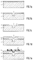
- FIG. 1 a - i are schematic representations of a number of steps in the method according to the invention.
- Fig. 1a shows a substrate 1 of glass, quartz glass in the present example, carrying a layer of molybdenum 2 having a thickness of 0.6 ⁇ m.
- molybdenum can be replaced by, for example, titanium or silicon.
- the layer is provided by means of sputtering. If silicon is used, the layer may also be applied by, for example, chemical deposition from the vapour phase.
- a photoresist pattern is formed using a customary UV sensitive photoresist material on the basis of novolak, and by means of UV contact exposure and local dissolution in a diluted solution of NaOH in water. Apertures are etched in the molybdenum layer according to a pattern by means of a mixture of phosphoric acid and nitric acid. Subsequently, a groove 3 is formed in the substrate 1 by means of reactive ion etching (anisotropic), said groove having a diameter of, for example, 6 x 6 ⁇ m, see Fig. 1b.
- the molybdenum is removed along the edges of the grooves, again by means of a photoresist, exposure and local dissolution, see Fig. 1c, which step may be carried out with a relatively low accuracy as regards width and position, i.e. in comparison with the step in which the grooves are formed.
- the width of the molybdenum-free track 4 amounts to approximately 20 ⁇ m.
- a layer of silicon dioxide 5 having a thickness of 7 ⁇ m is applied by means of high-frequency sputtering (frequency 13.6 MHz) in an argon atmosphere at a pressure of 3 Pa, see Fig. 1d).
- the target plate consists of quartz glass.
- the material deposited obtains a higher refractive index than the substrate material due to the use of a relatively high argon pressure and by applying a bias voltage to the substrate, for example a voltage of 20% of the voltage between the target plate and the substrate plate.
- a high refractive index can also be obtained by using a target plate consisting of silicon dioxide with a germanium-dioxide doping.
- the groove 3 is filled completely.
- the surface of the layer 5 may have recesses 6 at the location of the groove, in particular at locations where grooves intersect or meet. The differences in height generally amount to less than 6 ⁇ m.
- An adhesive layer 7 of molybdenum with a thickness of 35 nm is provided by means of sputtering. Said adhesive layer is coated with a protective layer 8 of a photoresist which is exposed according to a pattern and developed, after which the molybdenum released is removed. The glass layer 5 remains covered at the location of the grooves, see Fig. 1e), a relatively low positional accuracy being sufficient.
- the width of the protective layer 8 is larger than the corresponding aperture in the stop layer 2.
- the unprotected parts of the glass layer 5 are dissolved by means of wet chemical etching in hydrofluoric acid (concentration 4% of HF, preferably in a buffer solution), the molybdenum layer 2 serving as a stop layer for the etching process, see Fig. 1f), for which reason the etching time is not critical. Subsequently, the residual photoresist and molybdenum are removed by dissolving them in acetone and a mixture of phosphoric acid and nitric acid, respectively, see Fig. 1g).
- the intermediate product thus obtained is a flat substrate containing raised portions in a small part of its surface. These are removed by polishing using suspension of SiO2 particles having dimensions of approximately 20 nm in a NaOH solution having a pH-value of approximately 10.5, see Fig. 1h). As soon as the raised portions have been removed, the effectiveness of the polishing operation decreased rapidly so that a flat surface is obtained, the decrease of the substrate thickness being considerably less than 1 ⁇ m.
- a protective layer 10 of quartz glass is provided, see Fig. 1i), for example, in a customary manner by means of chemical deposition from the vapour phase and using a plasma so that a high deposition rate can be obtained.
- the composition of the protective layer is selected so that the refractive index is smaller than that of the material used to fill up the grooves.
- the material provided by chemical deposition is fused into a homogeneous layer at a temperature which is lower than the temperature at which the glass of the optical waveguide can deform, for example at 1100 to 1200° C.
- the latter step is superfluous if the protective layer is provided by means of chemical deposition from the vapour phase under the influence of a plasma.
- the method is conducted in the same way as in the preceding example; the glass layer 5, however, being formed by means of chemical deposition from the vapour phase, to which end SiCl4, GeCl4 and oxygen and/or water vapour are introduced into a reactor.
- the glass particles deposited are fused into a glass layer at a temperature of from 1400 to 1500° C.
- a nitrogen doping may alternatively be used to ensure that the glass layer 5, which will form the core glass of the optical waveguide, obtains a higher refractive index than the substrate material and the coating material.
- the adhesive layer 7 of molybdenum can be replaced by another adhesive layer, for example, of hexamethyldisilazane.
- the substrate 1 consisting of a fluorine-doped layer of quartz glass having a thickness of 20 ⁇ m, which is provided on a quartz- glass carrier by means of chemical deposition from the vapour phase under the influence of a plasma.
- the glass layer 5 is formed by high-frequency sputtering using a target plate of quartz glass which may now have the same refractive index than the carrier (not shown in the drawing) to which the fluorine-doped substrate layer is applied.
- Optical waveguides manufactured by the method according to the invention can suitably be used as single-mode light conductors.
- the choice of the groove pattern permits waveguides to be split or united in known manner so as to manufacture a planar optical component.
Landscapes
- Physics & Mathematics (AREA)
- Engineering & Computer Science (AREA)
- Microelectronics & Electronic Packaging (AREA)
- General Physics & Mathematics (AREA)
- Optics & Photonics (AREA)
- Optical Integrated Circuits (AREA)
- Surface Treatment Of Glass (AREA)
Applications Claiming Priority (2)
| Application Number | Priority Date | Filing Date | Title |
|---|---|---|---|
| NL8701478 | 1987-06-25 | ||
| NL8701478A NL8701478A (nl) | 1987-06-25 | 1987-06-25 | Werkwijze voor het vervaardigen van een planaire optische component. |
Publications (1)
| Publication Number | Publication Date |
|---|---|
| EP0297652A1 true EP0297652A1 (de) | 1989-01-04 |
Family
ID=19850197
Family Applications (1)
| Application Number | Title | Priority Date | Filing Date |
|---|---|---|---|
| EP88201254A Withdrawn EP0297652A1 (de) | 1987-06-25 | 1988-06-17 | Verfahren zum Herstellen eines planaren optischen Elementes |
Country Status (4)
| Country | Link |
|---|---|
| US (1) | US4931077A (de) |
| EP (1) | EP0297652A1 (de) |
| JP (1) | JPS6418943A (de) |
| NL (1) | NL8701478A (de) |
Cited By (3)
| Publication number | Priority date | Publication date | Assignee | Title |
|---|---|---|---|---|
| US4994139A (en) * | 1988-08-16 | 1991-02-19 | U.S. Philips Corp. | Method of manufacturing a light-conducting device |
| CN1105927C (zh) * | 1997-07-15 | 2003-04-16 | 三星电子株式会社 | 均匀平面光波导的制造方法 |
| EP1182472A3 (de) * | 2000-08-23 | 2004-02-04 | Matsushita Electric Industrial Co., Ltd. | Optisches Element und Vrefahren zu seiner Herstellung |
Families Citing this family (10)
| Publication number | Priority date | Publication date | Assignee | Title |
|---|---|---|---|---|
| US5200029A (en) * | 1991-04-25 | 1993-04-06 | At&T Bell Laboratories | Method of making a planar optical amplifier |
| US5281305A (en) * | 1992-05-22 | 1994-01-25 | Northrop Corporation | Method for the production of optical waveguides employing trench and fill techniques |
| WO1998042628A1 (de) | 1997-03-26 | 1998-10-01 | Siemens Aktiengesellschaft | Verfahren zum herstellen eines glaskörpers mit mindestens einer ausnehmung |
| US7068870B2 (en) * | 2000-10-26 | 2006-06-27 | Shipley Company, L.L.C. | Variable width waveguide for mode-matching and method for making |
| WO2002095453A2 (en) * | 2000-12-14 | 2002-11-28 | Shipley Company, L.L.C. | Optical waveguide termination with vertical and horizontal mode shaping |
| US7251406B2 (en) * | 2000-12-14 | 2007-07-31 | Shipley Company, L.L.C. | Optical waveguide termination with vertical and horizontal mode shaping |
| US7158701B2 (en) * | 2001-02-21 | 2007-01-02 | Shipley Company, L.L.C. | Method for making optical devices with a moving mask and optical devices made thereby |
| US6912345B2 (en) * | 2001-03-30 | 2005-06-28 | Shipley Company, L.L.C. | Tapered optical fiber for coupling to diffused optical waveguides |
| CN1302307C (zh) * | 2001-11-08 | 2007-02-28 | 希普雷公司 | 光纤终端 |
| US7024082B2 (en) * | 2003-05-16 | 2006-04-04 | Eastman Kodak Company | Apparatus and method for forming an optical converter |
Family Cites Families (3)
| Publication number | Priority date | Publication date | Assignee | Title |
|---|---|---|---|---|
| JPS56135808A (en) * | 1980-03-28 | 1981-10-23 | Nippon Telegr & Teleph Corp <Ntt> | Manufacture of glass waveguide path for optical circuit |
| JPS57604A (en) * | 1980-06-03 | 1982-01-05 | Nippon Telegr & Teleph Corp <Ntt> | Formation of three-dimensionally disposed glass waveguide |
| JPS61121341A (ja) * | 1984-11-16 | 1986-06-09 | Mitsubishi Electric Corp | ガラスパツシベ−シヨン形半導体装置の製造方法 |
-
1987
- 1987-06-25 NL NL8701478A patent/NL8701478A/nl not_active Application Discontinuation
-
1988
- 1988-06-17 EP EP88201254A patent/EP0297652A1/de not_active Withdrawn
- 1988-06-22 US US07/210,058 patent/US4931077A/en not_active Expired - Fee Related
- 1988-06-23 JP JP63153667A patent/JPS6418943A/ja active Pending
Non-Patent Citations (3)
| Title |
|---|
| PATENT ABSTRACTS OF JAPAN, Band 2, Nr. 106, 31. August 1978, Seite 5556 E 78; & JP-A-53 70 839 (FUJITSU K.K.) 23-06-1978 * |
| PATENT ABSTRACTS OF JAPAN, Band 6, Nr. 8 (P-98)[886], 19. Januar 1982, Seite 142 P 98; & JP-A-56 135 808 (NIPPON DENSHIN DENWA KOSHA) 23-10-1981 * |
| PATENT ABSTRACTS OF JAPAN, Band 9, Nr. 292 (P-406)[2015], 19. November 1985, Seite 33 P 406; & JP-A-60 129 711 (OKI DENKI KOGYO K.K.) 11-07-1985 * |
Cited By (4)
| Publication number | Priority date | Publication date | Assignee | Title |
|---|---|---|---|---|
| US4994139A (en) * | 1988-08-16 | 1991-02-19 | U.S. Philips Corp. | Method of manufacturing a light-conducting device |
| CN1105927C (zh) * | 1997-07-15 | 2003-04-16 | 三星电子株式会社 | 均匀平面光波导的制造方法 |
| EP1182472A3 (de) * | 2000-08-23 | 2004-02-04 | Matsushita Electric Industrial Co., Ltd. | Optisches Element und Vrefahren zu seiner Herstellung |
| US6826344B2 (en) | 2000-08-23 | 2004-11-30 | Matsushita Electric Industrial Co., Ltd. | Optical element and method of fabrication thereof |
Also Published As
| Publication number | Publication date |
|---|---|
| US4931077A (en) | 1990-06-05 |
| NL8701478A (nl) | 1989-01-16 |
| JPS6418943A (en) | 1989-01-23 |
Similar Documents
| Publication | Publication Date | Title |
|---|---|---|
| US4931077A (en) | Method of manufacturing a planar optical component | |
| US4375312A (en) | Graded index waveguide structure and process for forming same | |
| JP2988916B2 (ja) | 光導波路の作製方法 | |
| EP0318267B1 (de) | Herstellungsverfahren für ein Bauteil der integrierten Optik | |
| US4554050A (en) | Etching of titanium | |
| CN1425147A (zh) | 自对准的混合工艺和元件 | |
| US5352566A (en) | Method of manufacturing optoelectronic components | |
| JPH0527132A (ja) | 導波路型光部品の製造方法 | |
| US6584807B1 (en) | Method of fabricating a component with crystalline silicon substrate | |
| CN1105927C (zh) | 均匀平面光波导的制造方法 | |
| EP1182468A2 (de) | Verfahren zur Herstellung einer Gitterstruktur auf einem Glassubstrat | |
| JPH09222525A (ja) | 光導波路の製造方法 | |
| JPS58117510A (ja) | 光導波路及びその製造方法 | |
| JP2663841B2 (ja) | 光結合構造の製造方法 | |
| JP3031066B2 (ja) | 酸化膜の製造方法及び光導波路の製造方法 | |
| US7095934B2 (en) | Optical waveguide manufacturing method | |
| JP2738121B2 (ja) | 石英系光導波路の製造方法 | |
| JP3139300B2 (ja) | ガラス導波路素子の製造方法 | |
| JPH05307125A (ja) | 光導波路の製造方法 | |
| JPH0843654A (ja) | 石英系ガラス導波路及びその製造方法 | |
| JPH05313032A (ja) | 光導波路の作製方法 | |
| JPH0473650A (ja) | 微細加工用マスク | |
| JPH08110426A (ja) | 光導波路の製造方法 | |
| JPH0933739A (ja) | 光導波路およびその製造方法 | |
| KR19990012248A (ko) | 광도파로 소자의 제작방법 |
Legal Events
| Date | Code | Title | Description |
|---|---|---|---|
| PUAI | Public reference made under article 153(3) epc to a published international application that has entered the european phase |
Free format text: ORIGINAL CODE: 0009012 |
|
| AK | Designated contracting states |
Kind code of ref document: A1 Designated state(s): DE FR GB NL |
|
| 17P | Request for examination filed |
Effective date: 19890622 |
|
| STAA | Information on the status of an ep patent application or granted ep patent |
Free format text: STATUS: THE APPLICATION IS DEEMED TO BE WITHDRAWN |
|
| 18D | Application deemed to be withdrawn |
Effective date: 19910103 |