EP0300414B1 - Methode zur Verbindung von Leitungen durch Verbindungslöcher - Google Patents
Methode zur Verbindung von Leitungen durch Verbindungslöcher Download PDFInfo
- Publication number
- EP0300414B1 EP0300414B1 EP88111550A EP88111550A EP0300414B1 EP 0300414 B1 EP0300414 B1 EP 0300414B1 EP 88111550 A EP88111550 A EP 88111550A EP 88111550 A EP88111550 A EP 88111550A EP 0300414 B1 EP0300414 B1 EP 0300414B1
- Authority
- EP
- European Patent Office
- Prior art keywords
- connection holes
- etching
- layer
- insulating layer
- holes
- Prior art date
- Legal status (The legal status is an assumption and is not a legal conclusion. Google has not performed a legal analysis and makes no representation as to the accuracy of the status listed.)
- Expired - Lifetime
Links
Images




Classifications
-
- H—ELECTRICITY
- H10—SEMICONDUCTOR DEVICES; ELECTRIC SOLID-STATE DEVICES NOT OTHERWISE PROVIDED FOR
- H10W—GENERIC PACKAGES, INTERCONNECTIONS, CONNECTORS OR OTHER CONSTRUCTIONAL DETAILS OF DEVICES COVERED BY CLASS H10
- H10W20/00—Interconnections in chips, wafers or substrates
- H10W20/01—Manufacture or treatment
- H10W20/071—Manufacture or treatment of dielectric parts thereof
- H10W20/081—Manufacture or treatment of dielectric parts thereof by forming openings in the dielectric parts
- H10W20/082—Manufacture or treatment of dielectric parts thereof by forming openings in the dielectric parts the openings being tapered via holes
-
- H—ELECTRICITY
- H10—SEMICONDUCTOR DEVICES; ELECTRIC SOLID-STATE DEVICES NOT OTHERWISE PROVIDED FOR
- H10P—GENERIC PROCESSES OR APPARATUS FOR THE MANUFACTURE OR TREATMENT OF DEVICES COVERED BY CLASS H10
- H10P50/00—Etching of wafers, substrates or parts of devices
- H10P50/20—Dry etching; Plasma etching; Reactive-ion etching
- H10P50/28—Dry etching; Plasma etching; Reactive-ion etching of insulating materials
- H10P50/282—Dry etching; Plasma etching; Reactive-ion etching of insulating materials of inorganic materials
- H10P50/283—Dry etching; Plasma etching; Reactive-ion etching of insulating materials of inorganic materials by chemical means
-
- H—ELECTRICITY
- H10—SEMICONDUCTOR DEVICES; ELECTRIC SOLID-STATE DEVICES NOT OTHERWISE PROVIDED FOR
- H10W—GENERIC PACKAGES, INTERCONNECTIONS, CONNECTORS OR OTHER CONSTRUCTIONAL DETAILS OF DEVICES COVERED BY CLASS H10
- H10W20/00—Interconnections in chips, wafers or substrates
- H10W20/01—Manufacture or treatment
- H10W20/031—Manufacture or treatment of conductive parts of the interconnections
- H10W20/056—Manufacture or treatment of conductive parts of the interconnections by filling conductive material into holes, grooves or trenches
Definitions
- the present invention relates to a method of connecting electric wirings through connection holes of integrated circuits according to the preamble of claim 1.
- the insulating layer for insulating the upper electric wiring from the lower electric wiring cannot be formed thinner than a predetermined thickness which therefore normally must have a thickness of about 0.5 ⁇ or more.
- the aspect ratio that is the ratio of the hole depth and the hole diameter of the connection holes has been increased.
- Electric wiring layers are normally formed by depositing a metal such as Al and Mo on the entire surface of a substrate by sputtering whereupon lithographic and etching procedures are performed.
- a metal such as Al and Mo
- the burying rate - that is the ratio of the deposited film thickness within the connection hole versus the deposited film thickness on the flat surface - is abruptly reduced when the aspect ratio as shown in Fig. 9, is increased to more than 1. This means that if the insulating layer cannot be made thin, the metal cannot be deposited sufficiently within the conncetion holes.
- the connection hole diameter becomes smaller than a predetermined value, a reliable conncetion to the electric wiring layer cannot be obtained.
- connection holes see f.i.: VSLI Electronics Microstructure Science Vol 1, p 12 and 13 and Vol 2, p 3-12.
- the simplest tapering method for opening the connection holes is by wet etching, which will be described with reference to Figs. 10A-C.
- an Al wiring 2 is formed on a semiconductor substrate 1 having a step 1a on its upper surface, whereupon a SiO2 layer 3 having a flat surface is formed thereon by the known bias sputtering method or the etch-back method.
- a resist layer 7 is then deposited by normal lithography in order to form a contact hole pattern.
- through holes 4 and 4′ having different depths are formed by wet etching thereby using a buffer hydrofluoric acid solution and the resist layer 7 as an etching mask.
- the taper angle 5 is about 45°.
- the pattern conversion difference - that is the difference in size between the resist layer 7 and the SiO2 layer 3 - becomes about twice as big on an upper surface of the through holes as their depth. Since the shallow through hole 4′ is in contact with the etching solution until the deep through hole 4 is formed, the pattern conversion difference is further increased on the bottom surface of the through hole. Since during wet etching, the etching rate depends on the material a certain amount of overetching must be performed in order to completely form through holes on the entire wafer surface. As a result, the conversion difference is further increased.
- connection holes are a method utilizing reactive ion etching (RIE) as dry etching.
- RIE reactive ion etching
- FIG. 10D the SiO2 layer 3 is then etched by anisotropic etching, whereby connection holes 4 und 4′ are formed having substantially vertical side walls.
- the RIE-procedure is performed on the entire surface using a gas mixture of C3F8 and H2.
- connection holes are tapered as show in Fig. 10E. Since polymerization and etching are used at the same time, and since the conditions of the polymerization are changed in accordance with the type and the history of an apparatus, the loading effect, the size and the density of a pattern and the like, a rather complex working procedure is required while at the same time the uniformity and the reproducibility of the product tends to be degraded. In addition the side walls of the connection holes cannot be tapered at an arbitrary angle, while differences of the pattern conversion of the connection hole bottom surfaces cannot be eliminated. Even if these difficulties are eliminated, a semiconductor device having a high manufacturing yield and reliability cannot be obtained.
- a SiO2 layer 2 is formed on an Si substrate 1 by a normal CVD or sputtering method.
- a connection hole 4 is then formed within the SiO2 layer 2 by lithographic and etching procedures.
- tungsten 14 is selectively grown within the connection hole 4. Since selectively grown tungsten 14 has a grain size of several 10 ⁇ 7 m , undulations of about 10 ⁇ 7 m are formed on its surface. In addition, the selective growth of tungsten is rather sensitive to the surface conditions of the substrate on which the tungsten is to be grown.
- the average grown film thickness of tungsten must be about 80 % or less of the depth of the connection holes.
- a metal layer 17 is deposited by a normal sputtering method, which later is formed to a wiring layer by normal lithographic and etching procedure.
- the wiring layer 17 must cover sufficiently the tungsten 14 within the connection hole 4.
- the aspect ratio is increased by recesses formed by the tungsten 14, the wiring layer 17 does not have a sufficient thickness in this areas so that the wiring resistance is largely increased due to this fact. In the worst case, disconnections may occurs.
- the tungsten selective growth method appears not to be satisfactory in order to form fine multi-layered wirings with a high yield and reliability.
- connection holes with different depths are present the above problems become even more serious.
- connection holes within the insulating layer of integrated circuits is known from JA-OS 59-189631 whereby the tapers within of the insulting layer are obtained by high frequency sputtering or ion milling, thereby using an inert gas such as Argon gas.
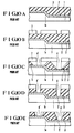
- Figs. 1A to 1E show an embodiment of a method of connecting wirings through connection holes according to the present invention.
- an Si substrate is used as a first conductive layer, and a second conductive layer is formed on the Si substrate through a connection hole, i.e., a contact hole.
- a connection hole i.e., a contact hole.
- an SiO2 layer 22 is formed on an Si substrate 21 serving as a first conductive layer by a normal CVD or sputtering method.
- a contact hole 23 is formed in the SiO2 layer 22 by lithography and etching.
- tungsten 24 is selectively grown as a metal column in the contact hole 23 to be thinner than a depth of the contact hole 23. Note that the above steps are the same as the conventional steps shown in Figs. 11A to 11C.
- a taper 26 is formed on a side wall of the contact hole 23 upward from a point 25 contacting an upper surface of the tungsten 24 using selective sputter etching by oxygen ions to be described later, as shown in Fig. 1D.
- an angle ⁇ of the taper 26 can be controlled to be an arbitrary value within the range of 0° ⁇ ⁇ ⁇ 90°. Therefore, in order not to excessively increase a hole diameter at the upper end of the contact hole 23 with respect to that at its lower end, the angle ⁇ of the taper 26 may be increased. Meanwhile, if the aspect ratio of the hole left on the tungsten 24 is so large as to cause disconnection of an upper wiring, the angle ⁇ of the taper 26 may be reduced.
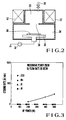
- a bias ECR (ELECTRON CYCLOTRON RESONANCE) etching method is used, and an apparatus therefor will be described below with reference to Fig. 2.
- a substrate electrode 32 connected to an RF bias power source 31 is disposed at a lower central portion in a sample chamber 34, and a sample substrate 36 is disposed thereon.
- a plasma generating chamber 33 is located above and adjacent to the sample chamber 34, and a window 38 is formed between the plasma generating chamber 33 and the sample chamber 34 so as to oppose the sample substrate 36.
- a gas supply mechanism 35 is formed above the plasma generating chamber 33 to supply an etching gas such as O2 gas or Ar gas.
- a magnet coil 37 is disposed around the plasma generating chamber 33 to efficiently transport ions generated in the plasma generating chamber 33 by a magnetic field to the sample chamber 34.
- a microwave electron cyclotron resonance method is used.
- an oxygen plasma can be generated at a high vacuum pressure of 1,33 * 10 ⁇ 2-1,33*10 ⁇ 3Pa. Therefore, a generation efficiency of oxygen ions is high and oxygen ions are further accelerated by applying an RF bias voltage to the substrate electrode 32. As a result, high-speed sputter etching by oxygen ions can be performed on the sample substrate 36.
- Fig. 3 shows RF power dependencies of etching rates of SiO2, Mo, W, and Al obtained by oxygen ions when the bias ECR etching apparatus in Fig. 2 is used.
- the RF power is plotted along the abscissa, and the etching rate is plotted along the ordinate.
- the etching rate of SiO2 is increased, but Mo, W, and Al are not etched.
- the metal is not etched unless the oxygen is sputter-etched by oxygen ions again. That is, the metal is not etched because the metal is immediately oxidized even if the oxygen is etched by sputtering.
- the tapered shape as shown in Fig. 1D is obtained by sputter etching using an O2 gas.
- the side wall of the contact hole 23 in Fig. 1C is tapered on the basis of a well-known incident angle dependency of a sputtering rate. That is, since etching ions are incident vertically on the sample substrate 36 in Fig. 2, the side wall of the contact hole 23 in Fig. 1C is not etched when the angle of the taper 26 in Fig. 1D is 90°.
- FIG. 5 A relationship between an ion incident angle and an etching rate with respect to the SiO2 layer 22 is well shown in Fig. 5.
- the SiO2 layer 22 is ion-etched at an etching rate indicated by arrow a.
- the incident angle is 0°
- ions are incident on a flat portion of the SiO2 layer 22. Therefore, the flat portion is etched at a certain rate.
- the taper is formed at the upper end corner portion of the contact hole 23, the ion incident angle at the portion is gradually increased, and the etching rate is increased.
- the etching rate is highest at an incident angle of about 45°.
- the SiO2 layer 22 is etched from a state indicated by broken lines to a state indicated by solid lines in Fig. 6. Since the ion incident angle on the side wall of the contact hole 23 is 90°, the etching rate is reduced to be almost 0 as is shown at a portion indicated by c in Fig. 5, i.e., the side wall is almost not etched. In addition, the metal portion (tungsten 24) is almost not etched as is apparent from a portion d of the characteristic shown in Fig. 5. As a result, in Fig. 6, the tungsten 24 is almost not or not etched at all.
- the taper 26 is formed from the point 25 at which the side wall of the contact hole 23 is in contact with the tungsten 24.
- the sputtering rate on the inclined surface an angle of the taper 26 is larger than 0° and smaller than 90°
- the angle ⁇ of the taper 26 is reduced while a film thickness of the SiO2 layer 22 is not reduced very much.
- a position of the point 25 of the taper 26 is almost not changed.
- the taper is formed when sputter etching is performed by Ar ions, the tungsten 24 in Fig. 1D is undesirably etched at the same time (Fig. 4). However, as in the above embodiment, when sputtering is performed by oxygen ions the tungsten 24 is not etched.
- the metal layer is deposited by a normal sputtering method or the like, and then the wiring layer 27 is formed as a second conductive layer by normal lithography and etching.
- the wiring layer 27 is conductively connected on the Si substrate 21 through the contact hole 23 including the tungsten 24.
- the taper 26 is formed on the side wall of the contact hole 23
- the wiring layer 27 can have a sufficient film thickness in the contact hole 23 even if the aspect ratio is high. For this reason, an increase in electrical resistance or disconnection in the contact hole 23 of the wiring layer 27 can be prevented. Therefore, according to the present invention, a semiconductor apparatus having fine connection holes with high manufacturing yield and reliability can be obtained.
- tungsten is used as a metal column in a connection hole, but another metal such as Mo or Al may be used.
- a selective growth method is used as a deposition method of the metal, but another method such as a combination of a normal CVD method and etch-back may be used.
- the bias ECR etching apparatus is used as an etching apparatus for forming a taper.
- a condition that an insulating film is etched by oxygen ions need only be satisfied. Therefore, it is a matter of course that an etching apparatus of another system not departing from this concept may be used.
- connection hole in which a metal column need not be buried because its depth is small is present together with other connection holes, the metal column need not be buried in this connection hole but only a taper may be formed in the connection hole by etching using oxygen ions. That is, a connection hole not according to the present invention or a connection hole partially according to the present invention may be present together with the connection hole according to the present invention without posing any problem.
- Figs. 7A to 7D show another embodiment of the present invention in which the metal column described above is not buried.
- an Al wiring 42 is formed as a first conductive layer on a semiconductor substrate 41 having a step 41a on its surface, and an SiO2 layer 43 is formed thereon as an insulating layer.
- through holes 44 and 44′ are formed as connection holes in the SiO2 layer 43 by lithography and etching.
- tapers are formed on side walls of the through holes 44 and 44′ by selective sputter-etching using oxygen ions, respectively, as shown in Fig. 7C. In this case, the tapers are formed as in the above embodiment.
- each of the contact holes 44 and 44′ is gradually etched from its upper end corner portion to form a predetermined taper.
- a taper angle ⁇ of the taper can be controlled to be an arbitrary value within the range of 0° ⁇ ⁇ ⁇ 90°. Therefore, in order not to excessively increase a hole diameter at the upper end of each of the through holes 44 and 44′ with respect to that at its lower end, the taper angle ⁇ may be increased. Meanwhile, if an aspect ratio of the through holes 44 and 44′ is large to cause disconnection of the upper wiring, the taper angle ⁇ may be reduced.
- the taper is formed from a point of the contact hole 44 contacting the first conductive layer 42. Therefore, the diameter of the contact hole 44′ is slightly larger than that at the start of formation.
- the bias ECR etching apparatus or the other known etching apparatuses are used as an apparatus for forming the taper.
- a metal layer is deposited by a normal sputtering method or the like, and a wiring layer 46 as a second conductive layer is formed by normal lithography and etching.
- the wiring layer 46 can have a sufficient film thickness in the through holes 44 and 44′ even if the aspect ratio is high.
- Figs. 8A and 8B show a modification of the embodiment in Figs. 7A to 7D, corresponding to Figs. 7C and 7D.
- a taper is formed from a portion of a contact hole 44′ contacting a first conductive layer 42. Therefore, in the contact hole 44, the taper is formed upward from a middle portion of a side wall.
Landscapes
- Internal Circuitry In Semiconductor Integrated Circuit Devices (AREA)
- Drying Of Semiconductors (AREA)
Claims (4)
- Methode zum Verbinden elektrischer Leitungen durch Verbindungslöcher in integrierten Schaltungen, enthaltend die folgenden Schritte:- Ausbilden einer ersten elektrisch leitenden Schicht für erste elektrische Leitungen (42) auf einem Substrat (41)- Ausbilden einer Isolierschicht (43) auf diesem Substrat (41)- Ausbilden von Verbindungslöchern (44, 44′) innerhalb dieser Isolierschicht (43), wobei diese Löcher konisch schräg zulaufende Seitenwände aufweisen, und- Ausbilden einer zweiten, metallischen, leitenden Schicht für zweite elektrische Leitungen (46) auf der Isolierschicht (43), die durch die konischen Verbindungslöcher (44, 44′) mit den ersten Leitungen (42) auf dem Substrat elektrisch verbunden sind,dadurch gekennzeichnet, daß die konische Schräge der Seitenwände der Verbindungslöcher (44, 44′) nach dem Ausbilden der Verbindungslöcher durch Einsatz einer selektiven Sputter-Ätztechnik mit Sauerstoffionen erhalten wird, wobei die Sauerstoffionen mit dem Material der ersten elektrischen Leitungsschicht reagieren, um darauf eine Metalloxidschicht auszubilden, und damit zu einem langsameren Ätzen dieser Leitungsschicht gegenüber der Isolierschicht (43) und zum konischen Schrägen der Seitenwände der Verbindungslöcher (44, 44′) führen.
- Methode gemäß Anspruch 1, dadurch gekennzeichnet, daß nach dem Ausbilden der Verbindungslöcher (44, 44′), jedoch vor dem konischen Schrägen der Seitenwände innerhalb dieser Verbindungslöcher (44, 44′) Metallsäulen gebildet werden.
- Methode gemäß Anspruch 1 oder 2, dadurch gekennzeichnet, daß die selektive Sputter-Ätztechnik mit Sauerstoffionen so ausgeführt wird, daß nur die oberen Teile der Verbindungslöcher (44) innerhalb der Isolierschicht (43) konisch geschrägt werden.
- Methode zum Verbinden elektrischer Leitungen durch Verbindungslöcher in integrierten Schaltungen, enthaltend die folgenden Schritte:- Benutzen einer Substratoberfläche als erste elektrische Leitungen (21)- Ausbilden einer Isolierschicht (22) auf dieser Substratoberfläche (21)- Ausbilden von Verbindungslöchern (23) innerhalb dieser Isolierschicht (22), wobei diese Löcher konisch schräg zulaufende Seitenwände (26) aufweisen, und- Ausbilden einer metallischen, leitenden Schicht für zweite elektrische Leitungen (27) auf der Isolierschicht (22), die durch die konischen Verbindungslöcher (23) mit den ersten elektrischen Leitungen (21) elektrisch verbunden sind,dadurch gekennzeichnet, daß nach dem Ausbilden der Verbindungslöcher (23), jedoch vor dem konischen Schrägen der Seitenwände (26), Metallsäulen (24) innerhalb dieser Verbindungslöcher (23) gebildet werden, und daß das konische Schrägen der Seitenwände (26) der Verbindungslöcher (23) durch Einsatz einer selektiven Sputter-Ätztechnik mit Sauerstoffionen erhalten wird, wobei die Sauerstoffionen mit den Metallsäulen (24) reagieren, um darauf ein Metalloxid auszubilden, und damit zu einem langsameren Ätzen dieser Metallsäulen (24) gegenüber der Isolierschicht (22) und zum konischen Schrägen der Seitenwände (26) der Verbindungslöcher (23) führen.
Applications Claiming Priority (4)
| Application Number | Priority Date | Filing Date | Title |
|---|---|---|---|
| JP62178977A JPH0680665B2 (ja) | 1987-07-20 | 1987-07-20 | 半導体装置の製造方法 |
| JP178977/87 | 1987-07-20 | ||
| JP185384/87 | 1987-07-27 | ||
| JP62185384A JP2563180B2 (ja) | 1987-07-27 | 1987-07-27 | 半導体装置の製造方法 |
Publications (2)
| Publication Number | Publication Date |
|---|---|
| EP0300414A1 EP0300414A1 (de) | 1989-01-25 |
| EP0300414B1 true EP0300414B1 (de) | 1994-10-12 |
Family
ID=26498979
Family Applications (1)
| Application Number | Title | Priority Date | Filing Date |
|---|---|---|---|
| EP88111550A Expired - Lifetime EP0300414B1 (de) | 1987-07-20 | 1988-07-18 | Methode zur Verbindung von Leitungen durch Verbindungslöcher |
Country Status (3)
| Country | Link |
|---|---|
| EP (1) | EP0300414B1 (de) |
| KR (1) | KR920002863B1 (de) |
| DE (1) | DE3851802T2 (de) |
Families Citing this family (5)
| Publication number | Priority date | Publication date | Assignee | Title |
|---|---|---|---|---|
| FR2677668B1 (fr) * | 1991-06-14 | 1993-10-15 | France Telecom | Procede de nettoyage de surfaces metalliques oxydees dans la fabrication de reseaux d'interconnexions et plaquettes pour de tels reseaux. |
| DE69219998T2 (de) * | 1991-10-31 | 1997-12-18 | Sgs Thomson Microelectronics | Verfahren zur Entfernung von Polymeren aus Sacklöchern in Halbleitervorrichtungen |
| USRE36475E (en) * | 1993-09-15 | 1999-12-28 | Hyundai Electronics Industries Co., Ltd. | Method of forming a via plug in a semiconductor device |
| US5409861A (en) * | 1993-09-15 | 1995-04-25 | Hyundai Electronics Industries Co., Ltd. | Method of forming a via plug in a semiconductor device |
| US5658829A (en) * | 1995-02-21 | 1997-08-19 | Micron Technology, Inc. | Semiconductor processing method of forming an electrically conductive contact plug |
Family Cites Families (1)
| Publication number | Priority date | Publication date | Assignee | Title |
|---|---|---|---|---|
| JPH069199B2 (ja) * | 1984-07-18 | 1994-02-02 | 株式会社日立製作所 | 配線構造体およびその製造方法 |
-
1988
- 1988-07-18 DE DE3851802T patent/DE3851802T2/de not_active Expired - Lifetime
- 1988-07-18 EP EP88111550A patent/EP0300414B1/de not_active Expired - Lifetime
- 1988-07-19 KR KR1019880008981A patent/KR920002863B1/ko not_active Expired
Non-Patent Citations (2)
| Title |
|---|
| J. J. APPL. PHYS., Proc. 1989 Intern. Symp. Micro Process Conference, pp. 213-216. * |
| J. VAC. SCI. TECHNOL. B, vol. 8, no. 3, pp. 529-532 (1990) * |
Also Published As
| Publication number | Publication date |
|---|---|
| DE3851802T2 (de) | 1995-02-09 |
| DE3851802D1 (de) | 1994-11-17 |
| EP0300414A1 (de) | 1989-01-25 |
| KR920002863B1 (ko) | 1992-04-06 |
| KR890002998A (ko) | 1989-04-12 |
Similar Documents
| Publication | Publication Date | Title |
|---|---|---|
| EP0063917B1 (de) | Verfahren zur Herstellung eines Halbleiterbauelements | |
| US5063175A (en) | Method for manufacturing a planar electrical interconnection utilizing isotropic deposition of conductive material | |
| KR930007836B1 (ko) | 반도체장치 및 그 제조방법 | |
| EP0129476B1 (de) | Planare verkettete Schaltung für integrierte Schaltkreise | |
| EP0524818B1 (de) | Mehrlagige Verbindungsstruktur für eine Halbleiter- vorrichtung und Verfahren zu ihrer Herstellung | |
| US5614765A (en) | Self aligned via dual damascene | |
| EP0373360B1 (de) | Verfahren und Struktur zur Herstellung einer Isolierung aus VLSI- und ULSI-Schaltungen | |
| US4377438A (en) | Method for producing semiconductor device | |
| US5320979A (en) | Method of connecting wirings through connection hole | |
| EP0555032B1 (de) | Halbleiter-Kontaktöffnungsstruktur und -verfahren | |
| US20020076918A1 (en) | Use of boron carbide as an etch-stop and barrier layer for copper dual damascene metallization | |
| US6313030B1 (en) | Method of making a conductive layer covering a hole of decreasing diameter in an insulation layer in a semiconductor device | |
| US6027994A (en) | Method to fabricate a dual metal-damascene structure in a substrate | |
| US6455921B1 (en) | Fabricating plug and near-zero overlap interconnect line | |
| US5933756A (en) | Fabrication process of a semiconductor device having a multilayered interconnection structure | |
| US6025276A (en) | Semiconductor processing methods of forming substrate features, including contact openings | |
| EP0300414B1 (de) | Methode zur Verbindung von Leitungen durch Verbindungslöcher | |
| US6218287B1 (en) | Method of fabricating a semiconductor structure | |
| EP0262719B1 (de) | Verfahren zur Herstellung einer Planarleiterbahn durch isotropes Abscheiden von leitendem Werkstoff | |
| US6258716B1 (en) | CVD titanium silicide for contact hole plugs | |
| JP2563180B2 (ja) | 半導体装置の製造方法 | |
| US5397743A (en) | Method of making a semiconductor device | |
| KR20020057552A (ko) | 반도체 집적 회로의 제조 방법 | |
| KR100352304B1 (ko) | 반도체 장치 및 그 제조 방법 | |
| JPH0680665B2 (ja) | 半導体装置の製造方法 |
Legal Events
| Date | Code | Title | Description |
|---|---|---|---|
| PUAI | Public reference made under article 153(3) epc to a published international application that has entered the european phase |
Free format text: ORIGINAL CODE: 0009012 |
|
| 17P | Request for examination filed |
Effective date: 19880729 |
|
| AK | Designated contracting states |
Kind code of ref document: A1 Designated state(s): DE |
|
| 17Q | First examination report despatched |
Effective date: 19910904 |
|
| GRAA | (expected) grant |
Free format text: ORIGINAL CODE: 0009210 |
|
| AK | Designated contracting states |
Kind code of ref document: B1 Designated state(s): DE |
|
| REF | Corresponds to: |
Ref document number: 3851802 Country of ref document: DE Date of ref document: 19941117 |
|
| PLBE | No opposition filed within time limit |
Free format text: ORIGINAL CODE: 0009261 |
|
| STAA | Information on the status of an ep patent application or granted ep patent |
Free format text: STATUS: NO OPPOSITION FILED WITHIN TIME LIMIT |
|
| 26N | No opposition filed | ||
| PGFP | Annual fee paid to national office [announced via postgrant information from national office to epo] |
Ref country code: DE Payment date: 20070727 Year of fee payment: 20 |