EP0300609A2 - Réseau local en forme d'anneau - Google Patents
Réseau local en forme d'anneau Download PDFInfo
- Publication number
- EP0300609A2 EP0300609A2 EP88305249A EP88305249A EP0300609A2 EP 0300609 A2 EP0300609 A2 EP 0300609A2 EP 88305249 A EP88305249 A EP 88305249A EP 88305249 A EP88305249 A EP 88305249A EP 0300609 A2 EP0300609 A2 EP 0300609A2
- Authority
- EP
- European Patent Office
- Prior art keywords
- node
- ring
- receive
- register
- packet
- Prior art date
- Legal status (The legal status is an assumption and is not a legal conclusion. Google has not performed a legal analysis and makes no representation as to the accuracy of the status listed.)
- Withdrawn
Links
Images


Classifications
-
- H—ELECTRICITY
- H04—ELECTRIC COMMUNICATION TECHNIQUE
- H04L—TRANSMISSION OF DIGITAL INFORMATION, e.g. TELEGRAPHIC COMMUNICATION
- H04L12/00—Data switching networks
- H04L12/28—Data switching networks characterised by path configuration, e.g. LAN [Local Area Networks] or WAN [Wide Area Networks]
- H04L12/42—Loop networks
- H04L12/422—Synchronisation for ring networks
-
- H—ELECTRICITY
- H04—ELECTRIC COMMUNICATION TECHNIQUE
- H04L—TRANSMISSION OF DIGITAL INFORMATION, e.g. TELEGRAPHIC COMMUNICATION
- H04L12/00—Data switching networks
- H04L12/28—Data switching networks characterised by path configuration, e.g. LAN [Local Area Networks] or WAN [Wide Area Networks]
- H04L12/42—Loop networks
- H04L12/427—Loop networks with decentralised control
- H04L12/43—Loop networks with decentralised control with synchronous transmission, e.g. time division multiplex [TDM], slotted rings
-
- H—ELECTRICITY
- H04—ELECTRIC COMMUNICATION TECHNIQUE
- H04L—TRANSMISSION OF DIGITAL INFORMATION, e.g. TELEGRAPHIC COMMUNICATION
- H04L12/00—Data switching networks
- H04L12/28—Data switching networks characterised by path configuration, e.g. LAN [Local Area Networks] or WAN [Wide Area Networks]
- H04L12/42—Loop networks
- H04L12/427—Loop networks with decentralised control
- H04L12/433—Loop networks with decentralised control with asynchronous transmission, e.g. token ring, register insertion
Definitions
- This invention relates to a local area network comprising a multiple node ring which is particularly useful for the communication of digitised audio in aircraft.
- each active node comprising a packet-long register permanently connected in the ring, the node having means for labelling each packet it transmits as either full or empty and having means for testing whether the packet being received is full or empty in accordance with the said labelling, and means for preventing the transmission of a packet of new data by that node unless the packet as received is empty.
- This form of ring is in effect a hybrid of a register-insertion ring and a slotted ring.
- care must be taken with the clocking of data into and out of the register or registers, particularly where there is a high bit rate and where the number of nodes is high.
- Data must not be lost between the operations of clocking in and clocking out, and neither must there be any jitter as a result of slightly different frequencies of clocking.
- the receive clock and the transmit clock are identical and locked onto the incoming data, this will lead to jitter and will eventually cause errors.
- the clocks in all the nodes could be made very accurate and not locked together, and even this would eventually cause errors as even the most accurate crystals have a finite difference.
- the purpose of the present invention is to overcome these problems of clocking data in ring-shaped networks of the type described.
- the invention provides a local area network comprising a multiple node ring in which each node has separate receive and transmit registers for the transfer from and to the ring of packets of a common length, a receive clock, data-locked to the receive data for clocking the receive register, and an independent transmit clock for clocking the transmit register, the transmit clock being triggered on at the instant that a predetermined portion of an input packet has been received in the receive register, by triggering means connected to the receive register.
- the transmit clock is free-running and the receive clock is data-locked and, to avoid data bunching within nodes and the consequential lose of some data, the start of transmitted data packets is triggered by a fixed point in the received packet.
- the said predetermined proportion of an input packet is defined by the position of a synchronisation bit located at the same position in all the packets, each node having means for detecting the synchronisation bit in the receive register.
- a dual-redundant, contra-rotating ring-shaped local area network for an aircraft communications control system transmits both digitised audio signals and control data in small packets from node to node.
- the number of nodes is 4, interconnected by the two rings A,B of which only ring A is normally connected.
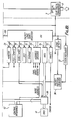
- the four nodes P,Q,R and S are each of the type illustrated in Figure 1, of which the portion to the right hand side of the broken vertical line constitutes the portion of the ring near the node, and the portion to the left hand side represents the means of accessing the ring at that node.
- the serial data transfer between nodes is achieved by way of a multi-mode optical fibre 2 which is terminated by 9mm SMA connectors.
- a pair of electrical to optical converters 3 constitute the interface at the node with the optical fibre 2, and operate at an optical wave length of for example 850nm, 1300nm or 1550nm.
- the bit rate of the ring is 20 Megabits per second with a tolerance of +/- 5 kilobits per second, and the transmission coding method for serial data transfer between nodes conforms to "Manchester II biphase".
- Each node comprises two shift registers, each precisely one packet in length, functioning as a receive register RX and a transmit register TX.
- Register RX bypasses register TX by means of a wire 100 and a switch 17, so that data is clocked selectively either from the receive register RX or from the transmit register TX.
- a packet assembly/disassembly section 13 ( Figures 3 and 6), represented by the portion of Figure 1 to the left hand side of the shift registers RX, TX, when required, reads the data from the receive register and writes data in the same format into the transmit register for transmission onto the ring.
- the packet format is as follows.
- the 28 bytes of each packet are divided into 4 bytes of overhead, known as the header message, and 24 bytes of information, either in the form of digitised audio or of control data.
- the first overhead byte is reserved for the synchronisation of packets, and is read by the synchronisation detector 36.
- the second overhead byte from a control field, of which the 8 bits include a monitor bit, a full/empty bit, a Jata/voice bit, a transmit/receive PTT bit, an override bit and a parity bit, whose functions will be described below, and which are detected by corresponding logic units 28 to 32 and 35.
- the third of the four overhead bytes contains a binary code indicating the address of the originating node, i.e. the node from which the packet was transmitted onto the ring, and is detected by an address decoder 33.
- the fourth of the overhead bytes contains a special address whose purpose is not essential to an understanding of the invention.
- the packet assembly/disassembly section 13 also comprises corresponding units 19 to 24 and 26 for setting the overhead bytes of the transmit register TX.
- Voice packets and data packets are distinguished by the setting of the data voice bit.
- the information section of either type of packet is read by an information reader 34, and is written into the transmit register by a corresponding information write unit 25.
- the information section of a voice packet contains 192 bits of digitally coded audio amounting to an elapsed time or not greater than two milliseconds.
- the information field in data packets provides the facility for selection, control and tuning of radios and encryptors at corresponding nodes of the network, or for down-loading built-in test information (BITI) or for the reconfiguration of a damaged ring and the reallocation of the monitor node, which functions will be described in greater detail below.
- BITI built-in test information
- Data buses carry the information bytes from the receive register RX to the information reader 34 and hence to the information write units 25 by way of two switches 39, 40 and a control interface 42.
- the information is bussed to an output FIFO register 41.
- the switch 40 is bussed from a latch 43 through the switch 40 to the information write unit 25.
- this change from an inactive state to an active state, is illustrated schematically by the movement of switches 15 and 16 from positions at which the wire 4 is connected into ring A, and the positions as illustrated in which the receive and transmit registers are connected instead in the ring A.
- the transmission of a packet from the transmit register TX is controlled so that it extends an inter-slot gap. This avoids any corruption of the data already on the ring. Similarly, for power-off, the switching process is reversed during an inter-slot gap.
- the receive clock is data-locked i.e. the clock for clocking data into the receive register RX is recovered from the incoming data stream. This is achieved by a clock recovery unit 37, using conventional techniques.
- the transmit clock is free-running, thus avoiding jitter which would otherwise occur between clocks of slightly different frequency.
- the transmission of data from the transmit register TX is started by a trigger provided by a packet position counter 38 which monitors the arrival of a predetermined bit of the packet into the receive register RX.
- the transmit clock generator 18 is triggered by a fixed point in the received packet. This is illustrated in Figure 3, in which the efforts ⁇ F1 and ⁇ F2 of the receive and transmit clock generators respectively, 37 and 18, are not equal, and the generated clock is independent from the recovered clock.
- All the packets are clocked in sequence into the receive register RX.
- the full/empty bit is monitored by the corresponding unit 29. If the packet is full, the originating address is compared by the address decoder 33 with the address of the node, provided by the control interface 42.
- the address decoder 33 then provides one of three outputs: "own”, “want” or “ignore”, depending respectively on whether the packet originated from the same node, the packet originated from an address with which the node wishes to communicate, and the packet originated from a node which is to be ignored.
- the switch 17 connects the receive register RX output via wire 100 to the ring, so that it acts as a repeater in the ring (with a delay), re-transmitting the packet unamended (except possibly for the monitor bit, to be described below). If the address decoder output is "ignore”, the information is not read from the register, but if it is “want” the information is read by the information read unit 34 and bussed to the FIFO unit 41.
- the switch 17 connects the transmit register TX instead to the ring, and the packet stored in the receive register RX is abandoned, to be overwritten by the next incoming packet.
- the transmit register TX transmits either a new, "full” packet or a "dummy" packet with the full/empty bit set to "empty” for subsequent destruction at the next node of the ring.
- the purpose of destroying "own" packets is to prevent packets being transmitted more than once around the ring.
- Packets found to be "empty” are treated in the same way as “own” packets: a new “full” packet, or, if no packet is awaiting transmission, an "empty" dummy packet is transmitted by the transmit, register TX. The original "empty" packet is abandoned in the receive register RX.
- damaged packets are monitored. This is achieved by appointing one of the nodes on the ring as a monitor node. All the nodes are capable of being the monitor node, and the monitor node is assigned as the first node on the ring to be powered up. However, should this node fail, a restart procedure is provided to reassign the monitor node function.
- a monitor mode controller 27 controls the monitor function; its input is taken from a monitor read/write unit 28 associated with the monitor bit of the receive register RX.
- the monitor mode controller is capable of setting the monitor bit of either of the registers RX, TX and the full/empty bit of the transmit register TX.
- the monitor mode controller 27 ensures that the monitor bit of all the packets transmitted from either register is set on. If any packet arriving at the monitor node is found to have its monitor bit set on, thus indicating that it has failed to have been removed by its originating node, then that packet shall be destroyed, by setting the full/empty bit to "empty". The packet will be overwritten in the receive register of the next node in the ring.
- the PTT and override functions demanded by switches on a control panel associated with the node, modify the manner in which packets are communicated between particular nodes, depending for example on the particular facility that an operator requires.
- Built in test information shall be transmitted onto the ring network from any node when it is requested via a data packet from the network.
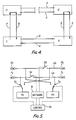
- each ring A,B has, in the region of the node illustrated, an electric wire 4A,4B interconnecting (via optical to electrical converters 3, Fig. 1) the optical fibre portions A1, A2; B1, B2.
- These wire connections may be broken by switches 5A, 5B, each corresponding to switch 5 of Figure 1, under the control of a network unit 51 operated by signals from a node control unit 50.
- the receive register RX is connectable, by a two-way switch S R controlled by the control unit 50, by further wires either to the wire 4B on the fibre portion B1 side of the switch 5B or to the wire 4A on the fibre portion A2 side of the switch 5A.
- the transmit register TX is connectable, by a two-way switch S t controlled by the control unit 50, by further wires either to the wire 4B on the fibre portion B2 side of the switch 5B or to the wire 4A on the fibre portion A1 side of the switch 5A.
- the switches S T and S R connect both the registers to the wire 4A of ring A; as shown in Figure 5.
- Each node's control unit 50 checks the status of "loopback" control bits in the packets it receives, to determine whether it is being requested by another node to reconfigure itself so as to "loop back" from ring A to ring B (or vice versa, if the packets are received from ring B). In the event that a loop back is required, the switch S T is changed so as to connect the transmit register TX to the other ring, which in the illustrated example is to ring B, on the fibre portion B2 side. This causes a loop back from the fibre portion A2 via the registers RX and TX to fibre portion B2.
- Loop back would occur, as illustrated in Figure 4, in the event of a fault between nodes P and Q in a network consisting of four nodes P,Q,R and S.
- the fault is remedied by reconfiguring the loop as shown, having loopbacks at nodes P and Q.
- Node Q fails to detect a signal from node P, or detects a constant stream of incorrect data from node P, and accordingly selects its own loopback switch so as to receive data from ring B instead of ring A, transmits a reconfiguration packet (with the "loopback" bits set appropriately) to node R, and waits a short time for a response from node R.
- Node R relays this reconfiguration packet to node S which relays a corresponding packet to node P.
- the procedure continues around the ring, until node P detects a failure to respond, at which point the control unit 50 of node P changes the appropriate loopback switch to connect its transmit register to ring B. This process takes no longer than one millisecond.
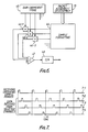
- each node generates its own frame period using the interval between its own samples, i.e. its own sample epoch. This is illustrated in Figure 7, in which the packets transmitted by the operator's node are shown as pulses in waveform 7-1, and those received from the selected channels, i.e. from selected nodes, are represented as corresponding pulses on three different waveforms 7-2, 7-3 and 7-4.
- the receiving node then assumes that all the packets from the network that appear within its own sample epoch occurred at the same instance. As shown in Figure 7, each group of three packets between adjacent pairs of broken lines are assumed to have occurred at the same instant. Assuming, for example, that each audio packet contains one sample, then for a 12KHz sample rate each node generates a packet ever 83 microseconds.
- the samples received from the packet assembly/disassembly section 13 are stored over a period of one sample epoch in a sample formatting unit 44.
- the sample formatting unit 44 provides a parallel output consisting of one output channel for each input channel, and each output channel is gain-adjusted in units 46-1, 46-2, 46-3 etc. by gain coefficients taken from a gain coefficient store 45.
- the gain-adjusted outputs are then summed in a summing unit 47 whose digital output is converted to an analogue audio signal in an digital-to-analogue converter 48.
Landscapes
- Engineering & Computer Science (AREA)
- Computer Networks & Wireless Communication (AREA)
- Signal Processing (AREA)
- Small-Scale Networks (AREA)
Applications Claiming Priority (2)
| Application Number | Priority Date | Filing Date | Title |
|---|---|---|---|
| GB8717365 | 1987-07-22 | ||
| GB08717365A GB2207327A (en) | 1987-07-22 | 1987-07-22 | Ring-shaped local area network |
Publications (2)
| Publication Number | Publication Date |
|---|---|
| EP0300609A2 true EP0300609A2 (fr) | 1989-01-25 |
| EP0300609A3 EP0300609A3 (fr) | 1990-03-28 |
Family
ID=10621121
Family Applications (1)
| Application Number | Title | Priority Date | Filing Date |
|---|---|---|---|
| EP88305249A Withdrawn EP0300609A3 (fr) | 1987-07-22 | 1988-06-09 | Réseau local en forme d'anneau |
Country Status (3)
| Country | Link |
|---|---|
| EP (1) | EP0300609A3 (fr) |
| JP (1) | JPH01112847A (fr) |
| GB (1) | GB2207327A (fr) |
Families Citing this family (3)
| Publication number | Priority date | Publication date | Assignee | Title |
|---|---|---|---|---|
| EP0462349B1 (fr) * | 1990-06-21 | 1995-02-22 | International Business Machines Corporation | Système de communication en anneau à large bande et méthode de commande d'accès |
| EP0575682B1 (fr) * | 1992-06-22 | 1998-08-26 | International Business Machines Corporation | Boítier central et interface pour boucle à jeton isochrone |
| RU2004946C1 (ru) * | 1992-12-28 | 1993-12-15 | Малое предпри тие "Инфонет" | Иерархическа сеть св зи |
Family Cites Families (4)
| Publication number | Priority date | Publication date | Assignee | Title |
|---|---|---|---|---|
| US4284843A (en) * | 1979-05-10 | 1981-08-18 | General Electric Company | Repeating station for use in digital data communications link |
| US4528661A (en) * | 1983-02-14 | 1985-07-09 | Prime Computer, Inc. | Ring communications system |
| JPS6086946A (ja) * | 1983-10-18 | 1985-05-16 | Yokogawa Hokushin Electric Corp | ル−プ形デ−タ通信システム |
| JPS619059A (ja) * | 1984-06-22 | 1986-01-16 | Oki Electric Ind Co Ltd | 再生中継装置 |
-
1987
- 1987-07-22 GB GB08717365A patent/GB2207327A/en not_active Withdrawn
-
1988
- 1988-06-09 EP EP88305249A patent/EP0300609A3/fr not_active Withdrawn
- 1988-07-21 JP JP18275088A patent/JPH01112847A/ja active Pending
Also Published As
| Publication number | Publication date |
|---|---|
| GB2207327A (en) | 1989-01-25 |
| JPH01112847A (ja) | 1989-05-01 |
| EP0300609A3 (fr) | 1990-03-28 |
| GB8717365D0 (en) | 1987-08-26 |
Similar Documents
| Publication | Publication Date | Title |
|---|---|---|
| US5345447A (en) | Switching hub which implements a virtual bus for interconnecting stations on a CSMA network | |
| US5818816A (en) | Communication device for switching connection from a working channel line to a protection channel line and vice versa | |
| KR860002213B1 (ko) | 루우프전송 시스템의 루우프-백 상태를 제어하는 루우프 전송시스템 및 방법 | |
| US4696001A (en) | Reconfigurable high-speed integrated local network | |
| HU219747B (hu) | Eljárás szinkronizálásra | |
| JPH0351142B2 (fr) | ||
| EP0533167A2 (fr) | Système de communication optique avec système de commutation des lignes de transmission | |
| EP0300778A2 (fr) | Réseau local en forme d'anneau | |
| US5875210A (en) | Method and apparatus for repeating data | |
| EP0300609A2 (fr) | Réseau local en forme d'anneau | |
| EP0300606A2 (fr) | Réseau local en forme d'anneau | |
| US4594724A (en) | Bypass method and apparatus for debouncing a mechanical switching element in a data communications network | |
| GB1561498A (en) | Loop communication system and a method of locating a fault in such system | |
| EP0300607A2 (fr) | Réseau local en forme d'anneau pour audio numérique | |
| US20050060394A1 (en) | Programmable delay, transparent switching multi-port interface line card | |
| JPS5927137B2 (ja) | デ−タ母線システム | |
| US7573902B2 (en) | Fibre channel interface unit | |
| US4858228A (en) | Communication system employing multi-conjunction architecture | |
| JP2544329B2 (ja) | 集線装置の診断および障害切離し方法 | |
| US4815072A (en) | Switching arrangements for digital telecommunications exchange systems | |
| GB2263043A (en) | Communication switching system and method | |
| JP2867865B2 (ja) | 予備回線切替制御方式 | |
| JPH02155340A (ja) | 予備ループを備えるループ状通信網 | |
| JPS6360938B2 (fr) | ||
| Schultze | Fault-tolerance in real-time communication |
Legal Events
| Date | Code | Title | Description |
|---|---|---|---|
| PUAI | Public reference made under article 153(3) epc to a published international application that has entered the european phase |
Free format text: ORIGINAL CODE: 0009012 |
|
| AK | Designated contracting states |
Kind code of ref document: A2 Designated state(s): DE FR IT |
|
| PUAL | Search report despatched |
Free format text: ORIGINAL CODE: 0009013 |
|
| AK | Designated contracting states |
Kind code of ref document: A3 Designated state(s): DE FR IT |
|
| STAA | Information on the status of an ep patent application or granted ep patent |
Free format text: STATUS: THE APPLICATION IS DEEMED TO BE WITHDRAWN |
|
| 18D | Application deemed to be withdrawn |
Effective date: 19901001 |