EP0300635A1 - Stromdetektoranordnung mit ferromagnetischem Magnetwiderstandselement - Google Patents
Stromdetektoranordnung mit ferromagnetischem Magnetwiderstandselement Download PDFInfo
- Publication number
- EP0300635A1 EP0300635A1 EP88306138A EP88306138A EP0300635A1 EP 0300635 A1 EP0300635 A1 EP 0300635A1 EP 88306138 A EP88306138 A EP 88306138A EP 88306138 A EP88306138 A EP 88306138A EP 0300635 A1 EP0300635 A1 EP 0300635A1
- Authority
- EP
- European Patent Office
- Prior art keywords
- magnetism sensing
- layer
- current
- conducting
- sensing layer
- Prior art date
- Legal status (The legal status is an assumption and is not a legal conclusion. Google has not performed a legal analysis and makes no representation as to the accuracy of the status listed.)
- Granted
Links
- 230000005294 ferromagnetic effect Effects 0.000 title claims abstract description 21
- 230000005389 magnetism Effects 0.000 claims abstract description 166
- 239000000758 substrate Substances 0.000 claims abstract description 62
- 230000005291 magnetic effect Effects 0.000 claims abstract description 37
- 238000005259 measurement Methods 0.000 claims description 22
- 239000004065 semiconductor Substances 0.000 claims description 8
- 230000004907 flux Effects 0.000 claims description 5
- 230000005355 Hall effect Effects 0.000 claims description 4
- 238000002955 isolation Methods 0.000 claims description 2
- 238000000034 method Methods 0.000 abstract description 8
- 230000000694 effects Effects 0.000 abstract description 7
- 230000035945 sensitivity Effects 0.000 abstract description 7
- 230000008859 change Effects 0.000 abstract description 2
- 238000000206 photolithography Methods 0.000 abstract description 2
- 239000010409 thin film Substances 0.000 description 9
- 229910052782 aluminium Inorganic materials 0.000 description 4
- 239000010408 film Substances 0.000 description 4
- 238000004544 sputter deposition Methods 0.000 description 4
- 238000010586 diagram Methods 0.000 description 3
- 238000005530 etching Methods 0.000 description 3
- 230000001747 exhibiting effect Effects 0.000 description 3
- WPYVAWXEWQSOGY-UHFFFAOYSA-N indium antimonide Chemical compound [Sb]#[In] WPYVAWXEWQSOGY-UHFFFAOYSA-N 0.000 description 3
- 229910003271 Ni-Fe Inorganic materials 0.000 description 2
- VYPSYNLAJGMNEJ-UHFFFAOYSA-N Silicium dioxide Chemical compound O=[Si]=O VYPSYNLAJGMNEJ-UHFFFAOYSA-N 0.000 description 2
- 229910045601 alloy Inorganic materials 0.000 description 2
- 239000000956 alloy Substances 0.000 description 2
- XAGFODPZIPBFFR-UHFFFAOYSA-N aluminium Chemical compound [Al] XAGFODPZIPBFFR-UHFFFAOYSA-N 0.000 description 2
- 238000000151 deposition Methods 0.000 description 2
- 229910001218 Gallium arsenide Inorganic materials 0.000 description 1
- 229910017709 Ni Co Inorganic materials 0.000 description 1
- 229910000990 Ni alloy Inorganic materials 0.000 description 1
- 229910003267 Ni-Co Inorganic materials 0.000 description 1
- 229910003262 Ni‐Co Inorganic materials 0.000 description 1
- 229910052581 Si3N4 Inorganic materials 0.000 description 1
- 229910052681 coesite Inorganic materials 0.000 description 1
- 229910052906 cristobalite Inorganic materials 0.000 description 1
- 238000001514 detection method Methods 0.000 description 1
- 238000001704 evaporation Methods 0.000 description 1
- 230000005352 galvanomagnetic phenomena Effects 0.000 description 1
- 238000010884 ion-beam technique Methods 0.000 description 1
- 238000004519 manufacturing process Methods 0.000 description 1
- 238000012986 modification Methods 0.000 description 1
- 230000004048 modification Effects 0.000 description 1
- PXHVJJICTQNCMI-UHFFFAOYSA-N nickel Substances [Ni] PXHVJJICTQNCMI-UHFFFAOYSA-N 0.000 description 1
- 230000008569 process Effects 0.000 description 1
- 230000004044 response Effects 0.000 description 1
- 229920006395 saturated elastomer Polymers 0.000 description 1
- 239000000377 silicon dioxide Substances 0.000 description 1
- 235000012239 silicon dioxide Nutrition 0.000 description 1
- 229910052682 stishovite Inorganic materials 0.000 description 1
- 229910052905 tridymite Inorganic materials 0.000 description 1
Images






Classifications
-
- G—PHYSICS
- G01—MEASURING; TESTING
- G01R—MEASURING ELECTRIC VARIABLES; MEASURING MAGNETIC VARIABLES
- G01R15/00—Details of measuring arrangements of the types provided for in groups G01R17/00 - G01R29/00, G01R33/00 - G01R33/26 or G01R35/00
- G01R15/14—Adaptations providing voltage or current isolation, e.g. for high-voltage or high-current networks
- G01R15/20—Adaptations providing voltage or current isolation, e.g. for high-voltage or high-current networks using galvano-magnetic devices, e.g. Hall-effect devices, i.e. measuring a magnetic field via the interaction between a current and a magnetic field, e.g. magneto resistive or Hall effect devices
- G01R15/205—Adaptations providing voltage or current isolation, e.g. for high-voltage or high-current networks using galvano-magnetic devices, e.g. Hall-effect devices, i.e. measuring a magnetic field via the interaction between a current and a magnetic field, e.g. magneto resistive or Hall effect devices using magneto-resistance devices, e.g. field plates
-
- G—PHYSICS
- G01—MEASURING; TESTING
- G01R—MEASURING ELECTRIC VARIABLES; MEASURING MAGNETIC VARIABLES
- G01R17/00—Measuring arrangements involving comparison with a reference value, e.g. bridge
- G01R17/10—AC or DC measuring bridges
- G01R17/105—AC or DC measuring bridges for measuring impedance or resistance
Definitions
- This invention relates generally to apparatus for measuring the amount of current flowing through a circuit, and particularly to current detecting device used for detecting current flowing through a circuit formed on a substrate.
- a coil is used for generating a magnetic field, and a current is detected by means of a detecting device such as a Hall generator and a magnetoresistor.
- a detecting device such as a Hall generator and a magnetoresistor.
- Fig. 24 shows an example of such a conventional current detecting device.
- a wire line 311 in which a current I′ flows, is inserted into a ring-shaped magnetic core 312 around which a coil 313 is wound, and a magnetic field H′ made by the current I′ is detected by measuring a potential difference between two terminals 314a and 314b of the coil 313.
- the reactance component of the coil 313 exists in the circuit through which a current, which is to be measured, is flowed thereby undesirably influencing input-output characteristics of the current measuring apparatus. Accordingly, it is difficult to produce a highly accurate current measuring apparatus.
- the coil 313 and the detecting device are difficult to unify as one body, the current measuring apparatus cannot be satisfactorily miniaturized.
- a further manufacturing step is required for adjusting a gap width between the coil 313 and the detecting device because the gap width is technically difficult to uniform in an assembly line.
- the present invention has been developed in order to remove the above-described drawbacks inherent to the conventional current detecting device.
- an object of the present invention to provide a new and useful current detecting device which can be produced by a photolithography technique using a ferromagnetic thin film.
- a current detecting device comprising: an insulating substrate; a magnetism sensing layer provided on the insulating substrate such that the insulating substrate is partially covered, both ends of the magnetism sensing layer being respectively connected to terminals of first two-terminal means for the measurement of the resistance of the magnetism sensing layer; an insulating layer provided on the magnetism sensing layer; and a conducting layer provided on the insulating layer such that the magnetism sensing layer is substantially located below the conducting layer when viewed from the conducting layer, both ends of the conducting layer being respectively connected to terminals of second two-terminal means for the application of a current to be measured.
- a current detecting device comprising: a magnetism sensing layer, both ends of the magnetism sensing layer being respectively connected to terminals of first two-terminal means for the measurement of the resistance of the magnetism sensing layer; an insulating layer provided around the magnetism sensing layer thereby forming a sensing member; and two conducting layers each provided at both sides of the sensing member such that the magnetism sensing layer is substantially interposed therebetween, the two conducting layers being connected at a first pair of ends of the sensing member thereby forming a current flowing member, both ends of the current flowing member being respectively connected to terminals of second two-terminal means for the application of a current to be measured.
- a current detecting device comprising: an insulating substrate; a magnetism sensing layer provided on the insulating substrate, one both ends of the magnetism sensing layer being respectively connected to terminals of first two-terminal means for the application of a constant current and the other both ends of the magnetism sensing layer being respectively connected to terminals of second two-terminal means for the measurement of a potential difference generated by Hall effect; and a conducting layer provided on the insurating substrate, both ends of the conducting layer being respectively connected to terminals of third two-terminal means for the application of a current to be measured.
- a current detecting device comprising: an insulating substrate; a conducting layer provided on the insulating substrate such that the insulating substrate is partially covered, both ends of the conducting layer being respectively connected to terminals of first two-terminal means for the application of a current to be measured; an insulating layer provided on the conducting layer; and a magnetism sensing layer provided on the insulating layer such that the conducting layer is substantially located below the magnetism sensing layer when viewed from the magnetism sensing layer, both ends of the magnetism sensing layer being respectively connected to terminals of second two-terminal means for the measurement of the resistance of the magnetism sensing layer.
- a current detecting device comprising: an insurating substrate; a magnetism sensing layer provided on the insulating substrate so as to extend in a first direction, both ends of the magnetism sensing layer being respectively connected to terminals of first two-terminal means for the measurement of the resistance of the magnetism sensing layer; a first insulating layer provided on the insurating substrate and the magnetism sensing layer; a first conducting layer provided on the first insulating layer so as to extend in a second direction making an angle of approximately 45° with the first direction, both ends of the first conducting layer being respectively connected to terminals of second two-terminal means for the application of a constant current; a second insulating layer provided on the first conducting layer; and a second conducting layer provided on the second insulating layer so as to extend in a third direction making the right angle with the second direction such that the magnetism sensing layer is arranged at the crossing portion of the first and second conducting layers when viewed from the second conducting layer, both ends of
- a current detecting device comprising: an insulating substrate; magnet means provided on one surface of the insulating substrate such that a line connecting N-pole with S-pole thereof extends in a first direction; a magnetism sensing layer provided on the other surface of the insulating substrate so as to extend in a second direction making an angle of approximately 45° with the first direction, both ends of the magnetism sensing layer being respectively connected terminals of first two-terminal means for the measurement of the resistance of the magnetism sensing layer; an insulating layer provided on the magnetism sensing layer such that the magnetism sensing layer is fully covered; and a conducting layer provided on the insulating layer so as to extend in the first direction, both ends of the conducting layer being respectively connected to terminals of second two-terminal means for the application of a current to be measured, whereby the magnet means, the magnetism sensing layer, and the conducting layer are overlapped.
- a current detecting device comprising: a substrate being connected to a first terminal; a conducting member provided on the substrate such that the conducting substrate is partially covered, the conducting member being connected to a second terminal, the first and second terminals formed first two-terminal means for the application of a current to be measured; an insulating layer provided on the substrate; and a magnetism sensing pattern having a plurality of radial line portions, both ends of the magnetism sensing pattern being respectively connected to terminals of second two-terminal means for the measurement of the resistance of the magnetism sensing pattern, the magnetism sensing pattern being provided on the insulating layer such that the conducting member is surrounded by the magnetism sensing pattern.
- a current detecting device comprising: a substrate; a conducting member, both ends of the conducting menber being respectively connected to terminals of first two-terminal means for the application of a current to be measured; a magnetism sensing member, both ends of the magnetism sensing member being respectively connected to terminals of second two-terminal means for the measurement of the resistance of the magnetism sensing member; and an insulating member for electrically the isolation between the conducting member and the magnetism sensing member whereby the conducting member, the magnetism sensing member, and the insulating member forms a detecting member, and the detecting member being formed on the substrate.
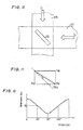
- the current detecting device comprises an insulating substrate 4, a magnetism sensing layer made of a magnetoresistor or a magnetoresistance element, i.e. a ferromagnetic magnetoresistance thin film 1, a thin insulating film 2 made by sputtering SiO2 or Si3N4, and a thin conducting film 3.
- a magnetism sensing layer made of a magnetoresistor or a magnetoresistance element, i.e. a ferromagnetic magnetoresistance thin film 1
- a thin insulating film 2 made by sputtering SiO2 or Si3N4, and a thin conducting film 3.
- the ferromagnetic magnetoresistance thin film 1 is formed by etching a magnetism sensing layer made by vapor-depoositing a nickel alloy such as Ni-Co and Ni-Fe on the insulating substrate 4, whereby insulating substrate is partially covered.
- the insulating thin film 2 is provided on the ferromagnetic magnetoresistance thin film 1, and the conducting thin film 3 is formed by etching a conducting layer made by vapor-depositing aluminum on the insulating thin film 2.
- the ferromagnetic magnetoresistance layer 1 is substantially located below the conducting layer 3 when viewed from the conducting layer 3.
- the magnetism sensing layer 1 and the conducting layer 3 are electrically isolated from each other.
- the ferromagnetic magnetoresistance thin film 1 can be made of an alloy mainly including Fe, Co, or Ni.
- the above-mentioned magnetoresistance element 1 has a property that its own resistance value varies when receiving a magnetic field in the direction making the right angle with a current flowing direction.
- a current flows toward an end portion 6 from an end portion 5 of the thin conducting film 3 as shown by an arrow I
- a magnetic field is generated in accordance with the intensity of the current.
- the magnetic field H is applied to the magnetic sensing layer 1 in the horizontal direction to the conducting layer 3 and in the direction making the right angle with the direction of the constant current.
- the resistance value of the magnetism sensing layer 1 varies in accordance with the intensity of the magnetic field received by the magnetism sensing layer 1 (magnetoresistance effect). Accordingly, the current value of the conducting layer 3 can be obtained by measuring the resistance value of the magnetism sensing layer 1.
- Terminals 7a and 8a are respectively connected to both ends of the magnetism sensing layer 1 for the. measurement of the resistance value of the magnetism sensing layer 1, and terminals 5a and 6a are respectively connected to both ends of the conducting layer 3 for the application of a current which is to be measured.
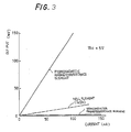
- Fig. 3 is a graph showing input-output characteristics of three elements of a ferromagnetic magnetoresistance element, a Hall generator, i.e. Hall element (InSb), and a semiconductor magnetoresistance element.
- the sensitivity of ferromagnetic magnetoresistance element is higher than those of others.
- the temperature coefficient of the ferromagnetic magnetoresistance element where the current is constant is -0.05%/°C; that of the Hall element is -0.13%/°C; and that of the semiconductor magnetoresistance element is -2%/°C. Therefore, the present current detecting device using a ferromagnetic magnetoresistance element exhibits satisfactory input-output characteristics.
- the current detecting device comprises an insulating substrate 11, conducting layers 12 and 16 which are made by evaporating aluminum and which are connected at one side thereof to each other thereby forming a current flowing member, and insulating layers 13 and 15 including a magnetism sensing layer 14 therebetween. Both ends of the current flowing member are respectively connected to terminals 18a and 18b for the application of a current which is to be measured, and both ends of the magnetism sensing layer 14 are also respectively connected to terminals 19a and 19b for the measurement of the resistance of the magnetism sensing layer 14.
- a first conducting layer 12 is formed on the insulating substrate 11 by using a photolithographic technique, and a first insulating layer 13 is formed on the first conducting layer 12 by sputtering method.
- the magnetism sensing layer 14 is provided by also vapor-depositing a ferromagnetic magnetoresistance element and by etching such an Al vapor-deposited layer.
- a second insulating layer 15 is formed on the magnetism sensing layer 14 by the sputtering method, and the second conducting layer 16 is provided on the second insulating layer 15.
- a contact hole 20 is made at one end portion thereof to connect the first conducting layer 12 with the second conducting layer 16 with the contact hole 20 being filled with Al.
- a second insulating layer 17 is provided on the second conducting layer 16.
- the magnetism sensing layer 14 is sandwiched between the insulating layers 13 and 15 thereby forming a sensing member, and the sensing member is sandwiched between the current flowing member.
- the magnetism sensing layer 14 is substantially interposed between the current flowing member.
- Fig. 6 is a top plan view of the current detecting device according to a third embodiment of the present invention
- Fig. 7 is a sectional view taken along line C-C of Fig. 6.
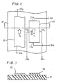
- the current detecting device comprises an insulating substrate 21, a conducting layer 22, a magnetism sensing layer 23. Both ends of the conducting layer 22 are respectively connected to terminals 22a and 22b for the application of a current I c which is to be measured.
- a first pair of opposing ends of the magnetism sensing layer 23 are respectively connected to terminals 24a and 24b for the application of a constant current i c in the direction of a dotted arrow of Fig.
- the conducting layer 22 and the magnetism sensing layer 23 are provided on the insulating substrate 21 such that the current Ic flows in the same flowing direction as the current i c .
- the magnetism sensing layer 23 can be made of InSb or GaAs, i.e. a device exhibiting Hall effect, and can be also made of a semiconductor magnetoresistance element such as InSb.
- the magnetism sensing layer 23 receives a magnetic field Hc whose direction is directed toward the plane of paper as indicated by a mark x, and when adopting a Hall element, a potential difference generates between the terminals 25a and 25b. It is to be noted that the direction of the potential difference makes the right angle with the flowing direction of current i c and the direction of the magnetic field Hc. Besides, when adopting a semiconductor magnetoresistance element, the current Ic can be measured by utilizing a property that the resistance of the semiconductor magnetoresistance element varies in accordance with the intensity of the magnetic field Hc.
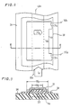
- a fourth embodiment of the current detecting device is shown in Figs. 8 and 9.
- the structure of the current detecting device is the same as the first embodiment except that a conducting layer 33 is located substantially below a magnetism sensing layer 31 when viewed from the magnetism sensing layer 31.
- Both ends of the conducting layer 33 are respectively connected to terminals 35a and 36a for the application of a current Id which is to be measured, and terminals 37a and 38a are respectively connected to both ends of the magnetism sensing layer 31.
- the current Id flows from the terminal 35a toward the terminal 36a
- the magnetism sensing layer 31 receives the magnetic field of Hd in the direction of an arrow. Therefore, the resistance between the terminal 37a and the terminal 38a varies in accordance with the intensity of the magnetic field Hd. As a result, the current Id can be measured by detecting the resistance therebetween.
- the pattern width of the conducting layer is WA
- the pattern width of the magnetism sensing layer is WM
- a preferable relation is obtained between WA and WM as follows.
- a changing rate of the resistance becomes large when a ratio WM/WA ⁇ 1.3, because the magnetic flux effectively passes through the magnetism sensing layer 31.
- the magnetic flux due to the current Id is effectively received by the magnetism sensing layer 31.
- the sensitivity of the current detecting device becomes high.
- a resistance value is R(0) when the current Id is 0mV
- a resistance value is R(50) when Id is 50mV
- the changing rate of the resistance is given by: (R(0) - R(50)) / R(0)
- Ni-Fe alloy is used as a magnetism sensing layer 31 for measuring the changing rate of the resistance.
- the change of the resistance between the both end portions 31a and 31b of the magnetism sensing layer 31 is very small because the intensity of the magnetic field Hd falls off at the inverse square of the distance between the conducting layer 33 and the magnetism sensing layer 31. Therefore, in the case of WM/WA > 1.3, the changing rate of the resistance is saturated.
- an operational amplifier is used in order to process a small signal indicative of a resistance value. Since the offset voltage of the operational amplifier is approximately 3mV or below in general, when the changing rate of the resistance is 0.3% or more, the current is detectable without any problem even if there is such an offset. Therefore, as shown in Fig. 10, the value of the ratio WM/WA is determined as 0.6 or more.
- Figs. 11 trough 13 show detecting circuits which can be used for the present current detecting device.
- the detecting circuit comprises a bridge circuit formed of the magnetism sensing layer 1 and resistors R1, R2, and R3, and a comparator 40.
- the terminal 8a is connected to one input terminal of the comparator 40, and a terminal electrode A′ is connected to the other input terminal of the comparator 40.
- the voltage of the terminal electrode A′ is desirably predetermined by adjusting the resistors R1 and R2, an outputted signal can be obtained when the voltage of the terminal 8a reaches the predetermined value.
- the detecting circuit comprises a bridge circuit formed of the magnetism sensing layer 1 and three resistors R4, R5, and R6, and two operational amplifiers 41 and 42.
- a terminal electrode B′ is connected to a noninverting input terminal of the operational amplifier 41 acting as a voltage follower, and the terminal 8a is connected to a noninverting input terminal of an operational amplifier 42 whose inverting input terminal is connected via a resistor R8 to the output terminal of the operational amplifier 41.
- the output terminal of the operational amplifier 42 is connected via a resistor R7 to the inverting input terminal of the operational amplifier 42.
- the bridge circuit can be formed by using two magnetism sensing layers 1 and resistors R9 and R10. In this case, there is an advantageous effect that the sensitivity of this circuit is doubled.
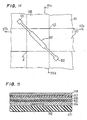
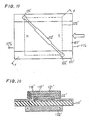
- the current detecting device comprises an insulating substrate 111, a magnetism sensing layer 112, two conducting layers 115 and 117, and three insulating layers 114, 116, and 118. Both ends of the magnetism sensing layer 112 are respectively connected to terminals 131 and 132 for the measurement of the resistance therebetween.
- the magnetism sensing layer 112 is provided on the insulating substrate 111 so as to extend in line, and a first insulating layer 114 is formed on the magnetism sensing layer 112 so as to cover the magnetism sensing layer 112.
- a first conducting layer 115 is provided on the first insulating layer 114, and both ends of the first conducting layer 115 are respectively connected to terminals 115a and 115b for the application of a constant current, or a bias current.
- a second insulating layer 116 is formed on the first conducting layer 115.
- a second conducting layer 117 is provided on the second insulating layer 116, and both ends of the second conducting layer 117 are respectively connected to terminals 117a and 117b for the application of a current which is to be measured, and a third insulating layer 118 is formed on the second conducting layer 117.
- the direction of the constant current I1 makes the right angle with the direction of the current I2 which is to be measured, and the magnetim sensing layer 112 is provided such that the magnetism sensing layer 112 effectively receives the magnetic fields of the currents I1 and I2.
- the magnetism sensing layer is formed at the crossing portion of the current flowing direction of the currents I1 and I2 when viewed from the third insulating layer 118.
- the magnetism sensing layer 112 extends so as to make an angle of approximately 45° with the both currents I1 and I2.
- the angle ⁇ varies in accordance with the intensity of the current I2 which is to be measured.
- Fig. 18 shows the relationship between the angle ⁇ and the resistance of the magnetism sensing layer 112. Accordingly the current I2 is measured by detecting the angle ⁇ . Furthermore, if the resistance value of the magnetism sensing layer 112, through which current I2 does not flow, is determined as a standard resistance value A1, the flowing direction of the current I2 is also detectable.
- Fig. 19 is a top plan view of the current detecting device according to a sixth embodiment of the present invention
- Fig. 20 is a sectional view taken along line F-F of Fig. 19.
- the current detecting device comprises an insulating substrate 111′, a permanent magnet 122′, a magnetism sensing layer 112′, a conducting layer 117′, and two insulating layers 118′ and 121′. Both ends of the magnetism sensing layer 112′ are respectively connected to terminals 131′ and 132′ for the measurement of the resistance value of the magnetism sensing layer 112′, and both ends of the conducting layer 117′ are respectively connected to terminals 117a and 117b for the application of a current which is to be measured.
- the permanent magnet 122′ is provided at one surface of the insulating substrate 111′ for applying a bias magnetic field, and the magnetism sensing layer 112′ is formed on the other surface of the insulating substrate 111′.
- the magnetism sensing layer 112′ is covered with a first insulating layer 122′, and the conducting layer 117′ is provided on the first insulating layer 122′.
- the magnetism sensing layer 112′ extends in a direction making an angle of approximately 45° with the flowing direction of the current I3, and a line connecting N-pole with S-pole of the permanent magnet 122′ extends the same direction as the flowing direction of the current I3 such that the permanent magnet 122′, the magnetism sensing layer 112′, and the conducting layer 117′ are overlapped. Therefore, the magnetism sensing layer 112′ effectively receives the magnetic fields of the permanent magnet 122′ and the current I3. As a result, the current I3 can be measured by the similar method to the fifth embodiment.
- an electromagnet can be also applied thereto.
- the current detecting device comprises a conducting substrate 221 made of Al, Co, or Si, a cylindrical conducting member 222 made of Al or Co, two insulating layers 223 and 226, and a wave-like magnetism sensing pattern 224 having a plurality of convex and concave portions alternately. More specifically, the magnetism sensing pattern has a plurality of radial line portions so that the magnetic flux passes therethrough in the direction making the right angle with the direction of a magnetic field H4.
- the cylindrical conducting member 222 is disposed on the conducting substrate 221 such that the conducting substrate 221 is partially covered, and the upper portion of the cylindrical conducting member 222 is connected to a first terminal 222a, and the remaning surface of the conducting substrate 221 is covered with a first insulating layer 223.
- the conducting substrate 221 is connected to a second terminal 222b, and the first and second terminals are used for the application of a current which is to be measured.
- the wave-like magnetism sensing pattern 224 is provided on the first insulating layer 223 such that the cylindrical conducting member 222 is surrounded by the wave-like magnetism sensing pattern 224, and two terminals 251 and 252 are respectively connected to both ends of the wave-like magnetism sensing pattern 224 for the measurement of the resistance therebetween.
- the thickness of the wave-like magnetism sensing pattern 224 is preferably determined to approximately 200-2000 angstroms.
- a second insulating layer 226 is provided on the wave-like magnetism sensing pattern 224.
- a magnetic field H4 When the current I4 flows from the terminal 222a to the terminal 222b, a magnetic field H4 generates around the cylindrical member 222 as shown in Fig. 21. At this time, the magnetic field H4 crosses a plurality of radial line portions of the wave-like magnetism sensing pattern 224. Accordingly, the resistance of the radial line portion is changed by the above-mentioned magnetoresistance effect in accordance with the intensity of the current I4. As a result, when the resistance of the wave-like magnetism sensing pattern 224 is detected, the current I4 can be measured. It is to be noted that since the resistance of the cylindrical member 222 can be small, it is able to flow a current of some amperes. As a result, the detection of a large current value can be achieved.
- the current detecting device of the seventh embodiment is formed with a power transistor 227 as one body.
- the power transistor 227 is formed on a lead frame 211, and an emitter electrode is surrounded by the wave-like magnetism sensing pattern 224. More specifically, an N+ collector layer 271 is formed on the lead frame 211, and an N ⁇ grown layer 272 is provided on the N+ collector layer 271.
- a P-type base region 273 is formed in the N ⁇ grown layer 272, and an N+ emitter region 274 is formed in the P-type base region 273.
- the insulating layer 223 is provided on the power transistor 227, and the wave-like magnetism sensing pattern 224 is disposed on the insulating layer 223 so as to position over the N+ emitter region 274.
- the insulating layer 226 is provided on the wave-like magnetism sensing pattern 224 and the insulatin layer 226, and a hole is made in the insulating layers 223 and 226 for connecting an emitter electrode 228 to the N+ emitter region 274 as shown in Fig. 23.
- the emitter electrode 228 is formed in the hole thereby the emitter electrode 228 is surrounded by the wave-like magnetism sensing pattern 224.
- base electrodes 229 are connected to the P-type base region 273 as shown in Fig. 23.
- the emitter current can be measured in the same way as that of the seventh embodiment.
- a semiconductor element such as FET and IGBT can be applied thereto.
Landscapes
- Physics & Mathematics (AREA)
- General Physics & Mathematics (AREA)
- Measuring Instrument Details And Bridges, And Automatic Balancing Devices (AREA)
- Hall/Mr Elements (AREA)
Applications Claiming Priority (6)
| Application Number | Priority Date | Filing Date | Title |
|---|---|---|---|
| JP168967/87 | 1987-07-07 | ||
| JP16896787 | 1987-07-07 | ||
| JP175063/87 | 1987-07-14 | ||
| JP62175063A JPS6418068A (en) | 1987-07-14 | 1987-07-14 | Detecting device of current |
| JP62302706A JP2712206B2 (ja) | 1987-11-30 | 1987-11-30 | 電流検出装置 |
| JP302706/87 | 1987-11-30 |
Publications (2)
| Publication Number | Publication Date |
|---|---|
| EP0300635A1 true EP0300635A1 (de) | 1989-01-25 |
| EP0300635B1 EP0300635B1 (de) | 1995-09-13 |
Family
ID=27323099
Family Applications (1)
| Application Number | Title | Priority Date | Filing Date |
|---|---|---|---|
| EP88306138A Expired - Lifetime EP0300635B1 (de) | 1987-07-07 | 1988-07-06 | Stromdetektoranordnung mit ferromagnetischem Magnetwiderstandselement |
Country Status (3)
| Country | Link |
|---|---|
| US (1) | US4937521A (de) |
| EP (1) | EP0300635B1 (de) |
| DE (1) | DE3854457T2 (de) |
Cited By (5)
| Publication number | Priority date | Publication date | Assignee | Title |
|---|---|---|---|---|
| EP0415439A3 (en) * | 1989-09-01 | 1992-03-04 | Kabushiki Kaisha Toshiba | Composite semiconductor device having function for overcurrent detection |
| EP0539081A1 (de) * | 1991-10-22 | 1993-04-28 | Hitachi, Ltd. | Stromsensorsystem oder Methode zur Stromerfassung |
| WO1995009447A1 (fr) * | 1993-09-27 | 1995-04-06 | Commissariat A L'energie Atomique | Capteur de courant comprenant un ruban magnetoresistif et son procede de realisation |
| EP0703460A1 (de) | 1994-09-26 | 1996-03-27 | CROUZET Automatismes | Magnetoresistiver Strommesser |
| US5717327A (en) * | 1995-09-22 | 1998-02-10 | Bradford; Melvin J. | Current sensor |
Families Citing this family (32)
| Publication number | Priority date | Publication date | Assignee | Title |
|---|---|---|---|---|
| US5262666A (en) * | 1989-05-15 | 1993-11-16 | Nippondenso Co., Ltd. | Semiconductor device with a nickel alloy protective resistor |
| US5216405A (en) * | 1991-01-14 | 1993-06-01 | General Motors Corporation | Package for the magnetic field sensitive device |
| DE4121374C2 (de) * | 1991-06-28 | 2000-09-07 | Lust Electronic Systeme Gmbh | Kompensierter Magnetfeldsensor |
| US5422566A (en) * | 1993-06-01 | 1995-06-06 | Westinghouse Electric Corporation | Apparatus and method for sensing DC current in a conductor |
| US6392400B1 (en) | 1998-10-08 | 2002-05-21 | Schlumberger Resource Management Services | High linearity, low offset interface for Hall effect devices |
| DE10013345B4 (de) | 2000-03-17 | 2004-08-26 | Sauer-Danfoss Holding Aps | Einrichtung zum Messen eines durch eine Leiterbahn fließenden elektrischen Stroms und deren Anwendung |
| DE10127754B4 (de) * | 2001-06-07 | 2014-11-20 | Robert Bosch Gmbh | Magnetoresistive Schichtanordnung |
| US6949927B2 (en) | 2001-08-27 | 2005-09-27 | International Rectifier Corporation | Magnetoresistive magnetic field sensors and motor control devices using same |
| US7259545B2 (en) * | 2003-02-11 | 2007-08-21 | Allegro Microsystems, Inc. | Integrated sensor |
| US7239123B2 (en) * | 2003-10-09 | 2007-07-03 | Hewlett-Packard Development Company, L.P. | Multiplexed dual-purpose magnetoresistive sensor and method of measuring current and temperature |
| US20050225282A1 (en) * | 2004-04-13 | 2005-10-13 | Scott Dewey | Giant magnetoresistive cell monitoring |
| US7777607B2 (en) * | 2004-10-12 | 2010-08-17 | Allegro Microsystems, Inc. | Resistor having a predetermined temperature coefficient |
| US7768083B2 (en) * | 2006-01-20 | 2010-08-03 | Allegro Microsystems, Inc. | Arrangements for an integrated sensor |
| US7388372B2 (en) * | 2006-05-31 | 2008-06-17 | Caterpillar Inc. | Electrical system with magnetoresistive sensors |
| US7528592B2 (en) * | 2006-05-31 | 2009-05-05 | Caterpillar Inc. | Magnetoresistive sensor for current sensing |
| US7795862B2 (en) | 2007-10-22 | 2010-09-14 | Allegro Microsystems, Inc. | Matching of GMR sensors in a bridge |
| JP2009229112A (ja) * | 2008-03-19 | 2009-10-08 | Tdk Corp | 電圧検出回路 |
| US7816905B2 (en) * | 2008-06-02 | 2010-10-19 | Allegro Microsystems, Inc. | Arrangements for a current sensing circuit and integrated current sensor |
| KR101825769B1 (ko) * | 2010-07-30 | 2018-03-22 | 꼼미사리아 아 레네르지 아토미끄 에뜨 옥스 에너지스 앨터네이티브즈 | 전압 또는 전류를 측정하기 위한 자기저항소자 통합 센서, 및 진단 시스템 |
| TWI428611B (zh) * | 2010-09-10 | 2014-03-01 | Ind Tech Res Inst | 零偏壓式功率偵測器 |
| JP5794777B2 (ja) * | 2010-12-22 | 2015-10-14 | 三菱電機株式会社 | 半導体装置 |
| JP5540299B2 (ja) | 2011-01-11 | 2014-07-02 | アルプス・グリーンデバイス株式会社 | 電流センサ |
| CH708052B1 (de) * | 2013-05-07 | 2016-09-15 | Melexis Technologies Nv | Vorrichtung zur Strommessung. |
| US9581620B2 (en) * | 2014-02-06 | 2017-02-28 | Stmicroelectronics S.R.L. | Integrated semiconductor device comprising a hall effect current sensor |
| US9958482B1 (en) * | 2016-12-20 | 2018-05-01 | Allegro Microsystems, Llc | Systems and methods for a high isolation current sensor |
| US10935612B2 (en) | 2018-08-20 | 2021-03-02 | Allegro Microsystems, Llc | Current sensor having multiple sensitivity ranges |
| US11187764B2 (en) | 2020-03-20 | 2021-11-30 | Allegro Microsystems, Llc | Layout of magnetoresistance element |
| US11567108B2 (en) | 2021-03-31 | 2023-01-31 | Allegro Microsystems, Llc | Multi-gain channels for multi-range sensor |
| EP4130772B1 (de) | 2021-08-05 | 2025-07-23 | Allegro MicroSystems, LLC | Magnetoresistives element mit kompensiertem temperaturkoeffizienten von tmr |
| US11994541B2 (en) | 2022-04-15 | 2024-05-28 | Allegro Microsystems, Llc | Current sensor assemblies for low currents |
| US12248039B2 (en) | 2023-08-08 | 2025-03-11 | Allegro Microsystems, Llc | Interleaving sub-arrays of magnetoresistance elements based on reference directions to compensate for bridge offset |
| US12510611B2 (en) | 2023-11-07 | 2025-12-30 | Allegro Microsystems, Llc | TMR sensor having magnetic field generation for pillar stimulation |
Citations (3)
| Publication number | Priority date | Publication date | Assignee | Title |
|---|---|---|---|---|
| EP0021916A1 (de) * | 1979-06-06 | 1981-01-07 | COMMISSARIAT A L'ENERGIE ATOMIQUE Etablissement de Caractère Scientifique Technique et Industriel | Verfahren zur Überwachung des augenblicklichen Zustandes einer elektrischen Schaltung und insbesondere zur Auffindung einer Unterbrechung in dieser Schaltung |
| EP0030041A1 (de) * | 1979-11-27 | 1981-06-10 | LGZ LANDIS & GYR ZUG AG | Messwandler zum Messen eines insbesondere von einem Messstrom erzeugten Magnetfeldes |
| EP0107059A1 (de) * | 1982-10-01 | 1984-05-02 | General Electric Company | Stromsensor |
Family Cites Families (4)
| Publication number | Priority date | Publication date | Assignee | Title |
|---|---|---|---|---|
| US4024489A (en) * | 1975-11-18 | 1977-05-17 | International Business Machines Corporation | Magnetoresistive sandwich including sensor electrically parallel with electrical shunt and magnetic biasing layers |
| JPS6046386B2 (ja) * | 1977-03-25 | 1985-10-15 | 日本電気株式会社 | 電流検出器 |
| JPS6180074A (ja) * | 1984-09-28 | 1986-04-23 | Toshiba Corp | 電流検出用端子付き磁気センサ |
| JPS61225661A (ja) * | 1985-03-29 | 1986-10-07 | Mitsubishi Electric Corp | 電流センサ |
-
1988
- 1988-07-06 EP EP88306138A patent/EP0300635B1/de not_active Expired - Lifetime
- 1988-07-06 DE DE3854457T patent/DE3854457T2/de not_active Expired - Lifetime
- 1988-07-07 US US07/216,430 patent/US4937521A/en not_active Expired - Lifetime
Patent Citations (3)
| Publication number | Priority date | Publication date | Assignee | Title |
|---|---|---|---|---|
| EP0021916A1 (de) * | 1979-06-06 | 1981-01-07 | COMMISSARIAT A L'ENERGIE ATOMIQUE Etablissement de Caractère Scientifique Technique et Industriel | Verfahren zur Überwachung des augenblicklichen Zustandes einer elektrischen Schaltung und insbesondere zur Auffindung einer Unterbrechung in dieser Schaltung |
| EP0030041A1 (de) * | 1979-11-27 | 1981-06-10 | LGZ LANDIS & GYR ZUG AG | Messwandler zum Messen eines insbesondere von einem Messstrom erzeugten Magnetfeldes |
| EP0107059A1 (de) * | 1982-10-01 | 1984-05-02 | General Electric Company | Stromsensor |
Non-Patent Citations (3)
| Title |
|---|
| IBM TECHNICAL DISCLOSURE BULLETIN, vol. 18, no. 11, April 1976, pages 3847-3851, New York, US; J.S. FENG: "Self-biased magnetoresistive bridge configuration for current measurement" * |
| IBM TECHNICAL DISCLOSURE BULLETIN, vol. 18, no. 8, January 1976, pages 2745-2748, New York, US; C.H. BAJOREK et al.: "Magnetoresistive current sensor" * |
| RADIO FERNSEHEN ELEKTRONIK, vol. 34, no. 5, May 1985, pages 316-319, Berlin, DD; U. LOREIT et al.: "Magnetoresistive Sensoren in der Mess- und Speichertechnik" * |
Cited By (8)
| Publication number | Priority date | Publication date | Assignee | Title |
|---|---|---|---|---|
| EP0415439A3 (en) * | 1989-09-01 | 1992-03-04 | Kabushiki Kaisha Toshiba | Composite semiconductor device having function for overcurrent detection |
| EP0539081A1 (de) * | 1991-10-22 | 1993-04-28 | Hitachi, Ltd. | Stromsensorsystem oder Methode zur Stromerfassung |
| US5561366A (en) * | 1991-10-22 | 1996-10-01 | Hitachi, Ltd. | Current sensor system and detection method comprising magetoresistance element, biasing conductor and current measurement conductor on insulating substrate |
| WO1995009447A1 (fr) * | 1993-09-27 | 1995-04-06 | Commissariat A L'energie Atomique | Capteur de courant comprenant un ruban magnetoresistif et son procede de realisation |
| US5708407A (en) * | 1993-09-27 | 1998-01-13 | Commissariat A L'energie Atomique | Current sensor comprising a magnetoresistive tape and its production process |
| EP0703460A1 (de) | 1994-09-26 | 1996-03-27 | CROUZET Automatismes | Magnetoresistiver Strommesser |
| FR2725029A1 (fr) * | 1994-09-26 | 1996-03-29 | Crouzet Automatismes | Capteur de courant a magnetoresistance |
| US5717327A (en) * | 1995-09-22 | 1998-02-10 | Bradford; Melvin J. | Current sensor |
Also Published As
| Publication number | Publication date |
|---|---|
| DE3854457D1 (de) | 1995-10-19 |
| US4937521A (en) | 1990-06-26 |
| DE3854457T2 (de) | 1996-02-29 |
| EP0300635B1 (de) | 1995-09-13 |
Similar Documents
| Publication | Publication Date | Title |
|---|---|---|
| EP0300635A1 (de) | Stromdetektoranordnung mit ferromagnetischem Magnetwiderstandselement | |
| EP0286079B1 (de) | Sensor mit einem magneto-elektrischen Messwandler | |
| US4385273A (en) | Transducer for measuring a current-generated magnetic field | |
| US4823075A (en) | Current sensor using hall-effect device with feedback | |
| US6949927B2 (en) | Magnetoresistive magnetic field sensors and motor control devices using same | |
| KR100983128B1 (ko) | 이중목적센서로서 자기저항센서를 이용한 시스템 및 장치 | |
| EP0539081B1 (de) | Stromsensorsystem oder Methode zur Stromerfassung | |
| US20030042902A1 (en) | Thin-film magnetic field sensor | |
| US6191581B1 (en) | Planar thin-film magnetic field sensor for determining directional magnetic fields | |
| US20040150397A1 (en) | Magnetic sensor and method for manufacturing the same | |
| CN113167841B (zh) | 利用反常霍尔效应的磁传感器和霍尔传感器以及霍尔传感器的制造方法 | |
| US20060012459A1 (en) | Sensor and method for measuring a current of charged particles | |
| US4506220A (en) | Temperature compensated magnetoresistive effect thin film magnetic sensor | |
| US6700371B2 (en) | Three dimensional conductive strap for a magnetorestrictive sensor | |
| JPH06148301A (ja) | 磁気センサ | |
| JP2545926B2 (ja) | 電流検出器 | |
| JPH0293373A (ja) | 電流検出器 | |
| Takayama et al. | Integrated thin film magneto-impedance sensor head using plating process | |
| WO2002068979A1 (en) | Improved polarity sensitive magnetic sensors | |
| JP4308084B2 (ja) | 磁性体検出器 | |
| JP3144051B2 (ja) | 電流検出器 | |
| JP2962293B2 (ja) | コルビノ型磁気センサ | |
| JP2712206B2 (ja) | 電流検出装置 | |
| US20250180608A1 (en) | Magnetic sensor and current sensor | |
| Kvitkovic | Hall generators |
Legal Events
| Date | Code | Title | Description |
|---|---|---|---|
| PUAI | Public reference made under article 153(3) epc to a published international application that has entered the european phase |
Free format text: ORIGINAL CODE: 0009012 |
|
| AK | Designated contracting states |
Kind code of ref document: A1 Designated state(s): DE FR GB IT |
|
| 17P | Request for examination filed |
Effective date: 19890510 |
|
| 17Q | First examination report despatched |
Effective date: 19910930 |
|
| GRAA | (expected) grant |
Free format text: ORIGINAL CODE: 0009210 |
|
| AK | Designated contracting states |
Kind code of ref document: B1 Designated state(s): DE FR GB IT |
|
| ITF | It: translation for a ep patent filed | ||
| ET | Fr: translation filed | ||
| REF | Corresponds to: |
Ref document number: 3854457 Country of ref document: DE Date of ref document: 19951019 |
|
| RIN2 | Information on inventor provided after grant (corrected) |
Free format text: YOSHINO, YOSHIMI * KAKEHI, TATUYA * SAKURAI, HIROSHI * AO, KENICHI * ARASUNA, TOSHIKAZU * IZAWA, ICHIROH |
|
| PLBE | No opposition filed within time limit |
Free format text: ORIGINAL CODE: 0009261 |
|
| STAA | Information on the status of an ep patent application or granted ep patent |
Free format text: STATUS: NO OPPOSITION FILED WITHIN TIME LIMIT |
|
| 26N | No opposition filed | ||
| REG | Reference to a national code |
Ref country code: GB Ref legal event code: 746 Effective date: 19970116 |
|
| ITPR | It: changes in ownership of a european patent |
Owner name: OFFERTA DI LICENZA AL PUBBLICO;PUBBLICO |
|
| REG | Reference to a national code |
Ref country code: GB Ref legal event code: IF02 |
|
| PGFP | Annual fee paid to national office [announced via postgrant information from national office to epo] |
Ref country code: DE Payment date: 20070628 Year of fee payment: 20 |
|
| PGFP | Annual fee paid to national office [announced via postgrant information from national office to epo] |
Ref country code: GB Payment date: 20070704 Year of fee payment: 20 |
|
| PGFP | Annual fee paid to national office [announced via postgrant information from national office to epo] |
Ref country code: IT Payment date: 20070730 Year of fee payment: 20 |
|
| PGFP | Annual fee paid to national office [announced via postgrant information from national office to epo] |
Ref country code: FR Payment date: 20070710 Year of fee payment: 20 |
|
| REG | Reference to a national code |
Ref country code: GB Ref legal event code: PE20 Expiry date: 20080705 |
|
| PG25 | Lapsed in a contracting state [announced via postgrant information from national office to epo] |
Ref country code: GB Free format text: LAPSE BECAUSE OF EXPIRATION OF PROTECTION Effective date: 20080705 |