EP0703460A1 - Magnetoresistiver Strommesser - Google Patents
Magnetoresistiver Strommesser Download PDFInfo
- Publication number
- EP0703460A1 EP0703460A1 EP95410111A EP95410111A EP0703460A1 EP 0703460 A1 EP0703460 A1 EP 0703460A1 EP 95410111 A EP95410111 A EP 95410111A EP 95410111 A EP95410111 A EP 95410111A EP 0703460 A1 EP0703460 A1 EP 0703460A1
- Authority
- EP
- European Patent Office
- Prior art keywords
- magnetoresistance
- current
- conductor
- current sensor
- magnetoresistor
- Prior art date
- Legal status (The legal status is an assumption and is not a legal conclusion. Google has not performed a legal analysis and makes no representation as to the accuracy of the status listed.)
- Granted
Links
- 239000004020 conductor Substances 0.000 claims abstract description 88
- 239000000758 substrate Substances 0.000 claims abstract description 27
- 230000005294 ferromagnetic effect Effects 0.000 claims abstract description 3
- 230000005291 magnetic effect Effects 0.000 claims description 22
- XEEYBQQBJWHFJM-UHFFFAOYSA-N Iron Chemical compound [Fe] XEEYBQQBJWHFJM-UHFFFAOYSA-N 0.000 claims description 12
- PXHVJJICTQNCMI-UHFFFAOYSA-N Nickel Chemical compound [Ni] PXHVJJICTQNCMI-UHFFFAOYSA-N 0.000 claims description 12
- 230000010287 polarization Effects 0.000 claims description 9
- 229910052742 iron Inorganic materials 0.000 claims description 6
- 239000000463 material Substances 0.000 claims description 6
- 229910052759 nickel Inorganic materials 0.000 claims description 6
- 239000010409 thin film Substances 0.000 claims description 5
- 229910052709 silver Inorganic materials 0.000 claims description 3
- 239000004332 silver Substances 0.000 claims description 3
- 238000005259 measurement Methods 0.000 description 15
- 238000004519 manufacturing process Methods 0.000 description 9
- 238000004804 winding Methods 0.000 description 8
- 230000035945 sensitivity Effects 0.000 description 5
- 239000003302 ferromagnetic material Substances 0.000 description 3
- 239000011521 glass Substances 0.000 description 3
- 239000013598 vector Substances 0.000 description 3
- VYPSYNLAJGMNEJ-UHFFFAOYSA-N Silicium dioxide Chemical compound O=[Si]=O VYPSYNLAJGMNEJ-UHFFFAOYSA-N 0.000 description 2
- XUIMIQQOPSSXEZ-UHFFFAOYSA-N Silicon Chemical compound [Si] XUIMIQQOPSSXEZ-UHFFFAOYSA-N 0.000 description 2
- 238000007796 conventional method Methods 0.000 description 2
- 238000000034 method Methods 0.000 description 2
- 229910052710 silicon Inorganic materials 0.000 description 2
- 239000010703 silicon Substances 0.000 description 2
- 229910052814 silicon oxide Inorganic materials 0.000 description 2
- BQCADISMDOOEFD-UHFFFAOYSA-N Silver Chemical compound [Ag] BQCADISMDOOEFD-UHFFFAOYSA-N 0.000 description 1
- 238000013019 agitation Methods 0.000 description 1
- 239000000470 constituent Substances 0.000 description 1
- 230000008021 deposition Effects 0.000 description 1
- 238000001514 detection method Methods 0.000 description 1
- 230000000694 effects Effects 0.000 description 1
- 239000011810 insulating material Substances 0.000 description 1
- 238000003754 machining Methods 0.000 description 1
- 230000005415 magnetization Effects 0.000 description 1
- 238000012986 modification Methods 0.000 description 1
- 230000004048 modification Effects 0.000 description 1
Images

Classifications
-
- G—PHYSICS
- G01—MEASURING; TESTING
- G01R—MEASURING ELECTRIC VARIABLES; MEASURING MAGNETIC VARIABLES
- G01R15/00—Details of measuring arrangements of the types provided for in groups G01R17/00 - G01R29/00, G01R33/00 - G01R33/26 or G01R35/00
- G01R15/14—Adaptations providing voltage or current isolation, e.g. for high-voltage or high-current networks
- G01R15/20—Adaptations providing voltage or current isolation, e.g. for high-voltage or high-current networks using galvano-magnetic devices, e.g. Hall-effect devices, i.e. measuring a magnetic field via the interaction between a current and a magnetic field, e.g. magneto resistive or Hall effect devices
- G01R15/205—Adaptations providing voltage or current isolation, e.g. for high-voltage or high-current networks using galvano-magnetic devices, e.g. Hall-effect devices, i.e. measuring a magnetic field via the interaction between a current and a magnetic field, e.g. magneto resistive or Hall effect devices using magneto-resistance devices, e.g. field plates
Definitions
- the present invention relates to a current sensor. It applies more particularly to the production of a current microsensor in which the measurement of the current flowing in a primary conductor has no influence on this current.
- a first conventional method consists in using a winding system to measure the current flowing in a conductor.
- the current to be measured flows in a primary winding which is associated with a secondary winding crossed by a current which is measured.
- the actual measuring device is thus electrically isolated from the primary circuit.
- a current flows in the primary winding, this current creates a magnetic field which induces in the secondary winding a current proportional to the value of the current to be measured (the proportionality ratio depends on the ratio between the number of turns that the two windings).
- a disadvantage of such a winding sensor is that it has a large size by the presence of the windings.
- a second conventional method consists in using so-called magnetoresistive elements, one characteristic of which is to have a resistivity which varies in the presence of a magnetic field.
- magnetoresistive elements one characteristic of which is to have a resistivity which varies in the presence of a magnetic field.
- Such elements are especially known for applications requiring a measurement of a magnetic field, for example, for the detection of very weak magnetic field or in applications related to the magnetic read heads of a hard disk or to magnetic ticket offices.
- FIG. 1 represents a so-called HUNT magnetoresistance.
- a magnetoresistance consists of a magnetoresistive bar 1 made of a ferromagnetic material and cut parallel to the easy axis of magnetization of the material (axis XX 'along which the electronic agitation is oriented naturally).
- the two ends of the bar 1 are connected to a conductor 1 'while a magnetic field B is applied in the plane of the bar 1 and perpendicular to the axis XX' of the bar.
- This magnetic field B induces a variation in the resistivity between the ends of the bar 1. If the conductor 1 'is supplied by a current generator, this variation in resistivity results in a variation in the current Im which flows in the conductor 1'.
- This variation in resistivity is a simple function of the value of the magnetic field B.
- a current sensor which uses a thin film magnetoresistor to measure a current flowing in a conductor.
- a sensor is, for example, described in European patent application EP-A-0 300 635.
- a magnetoresistor is deposited on an insulating substrate near a conductor in which the current to be measured flows.
- a disadvantage of such a sensor is that it does not make it possible to determine the direction of the current to be measured when the magnetoresistance is arranged parallel to the conductor. Indeed, the variation of resistivity is the same for two currents of the same value but of opposite direction. Another drawback is that the measurements are liable to be distorted by thermal drifts of the magnetoresistance. In addition, since the resistance-field characteristic of a magnetoresistor can vary from one magnetoresistor to another in mass production, two sensors from the same manufacturing series can give different results.
- the magnetoresistor is conventionally placed with an angle of approximately 45 ° relative to the conductor in which the current to be measured flows.
- the value of the current is then determined by measuring the angle between the direction of the magnetoresistance and the direction of the magnetic field resulting from the magnetic field induced by the current to be measured and the magnetic field induced by an additional conductor in which a current flows. constant and which is perpendicular to the conductor in which the current to be measured flows.
- the direction of the current can then be deduced by a measurement of the resistance of the magnetoresistance.
- the present invention aims to overcome these drawbacks by proposing a magnetoresistance current sensor which allows precise measurement of both the value and the direction of the current.
- the invention also aims to ensure that this measurement uses only one quantity.
- the invention also aims to make the measurement independent of thermal drifts of the magnetoresistance.
- the invention also aims to allow good reproducibility of the characteristics of the sensor in mass production.
- the invention further aims to propose a sensor which can be produced both in the plane of the substrate and in its thickness.
- the present invention provides a current sensor flowing in a primary conductor deposited on a first face of an insulating substrate, comprising a magnetoresistor consisting of a ferromagnetic deposit in a thin layer parallel to a section of the primary conductor, and comprising a polarization conductor parallel to the magnetoresistor by a section of a length at least equal to that of the magnetoresistor and connected, by its two ends, to the terminals of a polarization source supplying a constant current fixed as a function of the characteristic field resistance of the magnetoresistor, said magnetoresistor being connected by its two ends to a voltmeter.
- the senor comprises a secondary conductor constituted by a conductive track which is parallel to the magnetoresistance by at least one section distant from a given value of the magnetoresistance, said secondary conductor being connected by its two ends at the terminals of a generator of a variable current intended to compensate for the magnetic field induced, in the magnetoresistance, by the current to be measured.
- said section of the primary conductor and said section of the secondary conductor are distant from the magnetoresistance by distances determined as a function of the operating current range desired for the sensor.
- said section of the bias conductor is interposed between the magnetoresistor and said section of the primary conductor, the magnetoresistor being interposed between said sections of the polarization and secondary conductors.
- said bias conductor is merged with said conductor secondary, said bias source being merged with said compensation generator which then delivers a current consisting of a constant component, fixed as a function of the resistance-field characteristic of the magnetoresistance, and of a variable component as a function of the aux voltage magnetoresistance terminals.
- said sections of the conductors as well as the magnetoresistance are deposited on the same face of the insulating substrate while being spaced from each other by determined distances.
- said sections of the conductors as well as the magnetoresistance are stacked with the interposition of layers of insulating substrate of determined thicknesses.
- said layers of insulating substrate are made of different materials.
- the magnetoresistance consists of a thin film deposit of iron / nickel.
- the magnetoresistance consists of a thin film deposit of iron / nickel / silver.
- a current sensor comprises a magnetoresistor 1 produced in the form of a layer of ferromagnetic material deposited on an insulating substrate 3.
- This magnetoresistor 1 is deposited parallel to a section 4 of a primary conductor 5 in which the current I to be measured flows and is placed at a distance D from the section 4.
- the primary conductor 5 consists of a conductive track deposited on the same face of the substrate 3 as the magnetoresistance 1 and comprises two input terminals 5A and 5B of the sensor.
- a bias conductor 9 of the magnetoresistor 1 is interposed between the section 4 of the primary conductor 5 and the magnetoresistor 1.
- This bias conductor 9 consists of a conductive track deposited on the same face of the substrate 3 as the primary conductor 5 and has, according to the invention, a section 10 parallel to the magnetoresistance 1.
- the conductor 9 is connected to a polarization generator (not shown) by its two end terminals 9A and 9B. The polarization generator supplies a constant current.
- bias conductor 9 One function of this bias conductor 9 is to shift the resistance-field characteristic of the magnetoresistor 1 without deforming it.
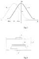
- FIG. 3 shows the characteristic of the resistance of a magnetoresistor as a function of the magnetic field, respectively in the absence of a polarization of the magnetoresistor 1 (curve A in solid lines) and in presence of a constant bias current Ip parallel to the magnetoresistance (curve B in dotted lines).
- the effect of the constant bias current Ip is to shift the resistance-field characteristic of the magnetoresistance 1.
- the magnetic field induced by a current I flowing in the conductor 5 modifies the resistance R with respect to a resistance value R0 which corresponds to the field H0 induced by the constant bias current Ip.
- the shift of the resistance-field characteristic of the magnetoresistor 1 can be carried out in one direction or the other depending on the direction of the bias current Ip.
- the section 10 is parallel to the magnetoresistor 1 allows that the offset of the resistance-field characteristic of the magnetoresistor 1 is not accompanied by a deformation of this characteristic.
- section 10 is parallel to the magnetoresistor 1 and to the section 4 of the primary conductor 5 eliminates any hysteresis and thus considerably improves the measurements, in particular for low values of current to be measured. It will be noted that such a parallel arrangement also makes it possible to produce the sensor in the plane of the substrate 3.
- the value Ip of the bias current as well as the distance between the section 10 of the bias conductor 9 and the magnetoresistor 1 are chosen so that the resistive response of the magnetoresistor 1, as a function of the magnetic field, is in a linear portion (for example , between Hmin and Hmax) of its characteristic. Placing the range of measurement in a linear portion of the resistance-field characteristic of magnetoresistance 1 optimizes the accuracy of the measurements and the resolution of the sensor. In addition, this linear portion being of steep slope, in particular thanks to the arrangement in parallel, one places oneself in an area of the characteristic where the sensitivity is the best, which gives optimal sensitivity to the sensor.
- a secondary conductor 2 in the form of a conductive track is also deposited on this same face of the substrate 3 on the other side of the magnetoresistance 1 relative to the primary conductor 5.
- the secondary conductor 2 comprises at least one section 6 which is parallel to magnetoresistor 1, at a distance d from magnetoresistor 1.
- the two terminals 2A and 2B of the secondary conductor 2 are connected to a variable current generator (not shown).
- the role of this current generator is to provide a current Is which compensates for the field induced by the current I flowing in the primary conductor 5.
- the current I is then proportional to the current Is, the proportionality coefficient being a function of the distances D and d which separate the magnetoresistance 1 from the conductors, respectively primary 5 and secondary 2.
- the relationship between the current I of the primary conductor 5 and the current Is of the secondary conductor 2, when the magnetic fields induced by the two conductors 5 and 2 compensate each other, is I Is * D / d.
- each end of the magnetoresistor 1 is connected by a conductive track 7 and 8 with two terminals, 1A and 1B respectively. These terminals 1A and 1B are intended to be connected to the terminals of a voltmeter (not shown).
- the voltage measured across the magnetoresistor 1 makes it possible to determine the value and the direction of the current Is which it is necessary to produce to compensate for the field induced by the current I.
- the voltage indicated by the voltmeter corresponds to the voltage at rest across the terminals of the magnetoresistor 1 (i.e.
- the value and the direction of the current Is make it possible to determine the value and the direction of the current I.
- the current Is is used when the voltage indicated by the voltmeter corresponds to the product of the constant bias current Ip and the resistance value R0.
- a secondary conductor 2 it allows a control of the measurement and makes this measurement independent, at the same time, of variations in the resistance-field characteristic of one magnetoresistance to another in mass production and of thermal drifts of magnetoresistance. The fact remains that, even in the absence of a secondary conductor 2, both the value and the direction of the current I can be determined from a single quantity.
- the choice of the distances D and d depends, in particular, on the current operating range of the sensor and, in particular, on the difference between the current values I to be measured and the operating range of the current generator supplying the current Is .
- the magnetoresistor 1 consists of a ferromagnetic material, for example of iron / nickel. It can also be provided that it is made of iron, nickel and silver, which improves its sensitivity.
- the bias conductor is merged with the secondary conductor 2.
- the variable current generator connected to terminals 2A and 2B of the conductor 2 modulates a non-zero current I0 (corresponding to the bias current Ip) as a function of the voltage across the terminals of magnetoresistance 1.
- this generator delivers a current Isp consisting of a constant component I0, fixed as a function of the resistance-field characteristic of magnetoresistance 1, and d a variable component Is, a function of the voltage across the terminals of magnetoresistance 1 to compensate for the magnetic field induced by the current to be measured I.
- the value I0 is determined in the same way as the value of the bias current Ip of the embodiment exposed in relation to FIG. 2 to shift the resistance-field characteristic of magnetoresistance 1.
- Figure 4 is a sectional view of a sensor constituting another aspect of the invention. Indeed, the invention provides also to realize the sensor no longer on a surface of an insulating substrate but in the thickness of a substrate.
- the senor consists of a stack of conductive layers in the thickness of the insulating substrate 3. At least one section 4 of the primary conductor is deposited on a first face of the substrate 3 while at at least one section 6 of the secondary conductor is deposited on a second face of the substrate 3. Between the two, in the thickness of the substrate 3, magnetoresistance 1 is produced and at least one section 10 of the bias conductor. In other words, the sensor is produced from an alternating stack of conductive layers 4, 10, 1, 6 and insulating layers 3. Although this is not visible in the sectional representation of FIG.
- the ratio between the primary and secondary currents is therefore fixed, in the embodiment represented in FIG. 4, by the duration of deposition of the materials constituting the stack and their machining, while in the embodiment exposed in relation to FIG. 2, this ratio is fixed by the process, generally photolithographic, of defining the tracks.
- An advantage of a flat sensor as shown in FIG. 2 is that the distance D between the section 4 of the conductor primary 5 and the magnetoresistance 1 may be greater for a substrate of the same nature (for example made of silicon).
- An advantage of a stacked sensor as shown in Figure 4 is that it offers better sensitivity.
- the plane in which the direct vectors of the induced magnetic field and of the current in the magnetoresistance are inscribed is perpendicular to the plane of the thin layer constituting the magnetoresistance.
- the magnetoresistance is therefore sensitive in its thickness (for example, of the order of a few micrometers).
- the plane in which the directing vectors are written is parallel to the plane of the layer constituting the magnetoresistance (for example, of the order of a few millimeters), which gives the sensor greater sensitivity.
- the directing vectors of the magnetic field induced by the current I and of the current in the magnetoresistance 1 are always perpendicular to each other.
- the insulating layers 3 can be made of the same material or of different materials. We can, for example, use silicon oxide, glass, or any other insulating material. The use of glass makes it possible, in particular, to provide greater thicknesses than with silicon oxide because of current technological limits. This increases the D / d ratio for measuring larger currents.
- the stacking can be carried out by placing the secondary conductor on a first face of a silicon substrate having a thickness of a few hundred micrometers (for example 300 ⁇ m).
- the magnetoresistance is produced from a second face of this substrate and is separated from the primary conductor by a glass thickness of the order of a few millimeters.
- the sensor proposed by the present invention is of simple constitution, and compact.
- the enslavement made by means of the secondary conductor 2 further simplifies the mass production of this sensor.
- the sensor according to the invention has a good resolution which allows precise measurements even for low currents while being able to have a large operating range in current to be measured.
Landscapes
- Physics & Mathematics (AREA)
- General Physics & Mathematics (AREA)
- Measuring Instrument Details And Bridges, And Automatic Balancing Devices (AREA)
Applications Claiming Priority (2)
| Application Number | Priority Date | Filing Date | Title |
|---|---|---|---|
| FR9411691 | 1994-09-26 | ||
| FR9411691A FR2725029A1 (fr) | 1994-09-26 | 1994-09-26 | Capteur de courant a magnetoresistance |
Publications (2)
| Publication Number | Publication Date |
|---|---|
| EP0703460A1 true EP0703460A1 (de) | 1996-03-27 |
| EP0703460B1 EP0703460B1 (de) | 2003-04-09 |
Family
ID=9467443
Family Applications (1)
| Application Number | Title | Priority Date | Filing Date |
|---|---|---|---|
| EP95410111A Expired - Lifetime EP0703460B1 (de) | 1994-09-26 | 1995-09-22 | Magnetoresistiver Strommesser |
Country Status (3)
| Country | Link |
|---|---|
| EP (1) | EP0703460B1 (de) |
| DE (1) | DE69530253T2 (de) |
| FR (1) | FR2725029A1 (de) |
Cited By (1)
| Publication number | Priority date | Publication date | Assignee | Title |
|---|---|---|---|---|
| WO2008012309A3 (de) * | 2006-07-26 | 2008-03-27 | Siemens Ag | Stromerfassungsvorrichtung und verfahren zur stromerfassung |
Families Citing this family (1)
| Publication number | Priority date | Publication date | Assignee | Title |
|---|---|---|---|---|
| JP3696448B2 (ja) * | 1999-09-02 | 2005-09-21 | 矢崎総業株式会社 | 電流検出器 |
Citations (3)
| Publication number | Priority date | Publication date | Assignee | Title |
|---|---|---|---|---|
| EP0300635A1 (de) | 1987-07-07 | 1989-01-25 | Nippondenso Co., Ltd. | Stromdetektoranordnung mit ferromagnetischem Magnetwiderstandselement |
| EP0315358A2 (de) * | 1987-10-30 | 1989-05-10 | Honeywell Control Systems Ltd. | Verfahren zur Herstellung eines Stromsensors |
| EP0539081A1 (de) * | 1991-10-22 | 1993-04-28 | Hitachi, Ltd. | Stromsensorsystem oder Methode zur Stromerfassung |
Family Cites Families (1)
| Publication number | Priority date | Publication date | Assignee | Title |
|---|---|---|---|---|
| DE69106334T2 (de) * | 1990-12-10 | 1995-05-04 | Hitachi Ltd | Mehrsicht Film mit magnetoresistiven Effekt und magnetoresitives Element. |
-
1994
- 1994-09-26 FR FR9411691A patent/FR2725029A1/fr active Granted
-
1995
- 1995-09-22 DE DE69530253T patent/DE69530253T2/de not_active Expired - Fee Related
- 1995-09-22 EP EP95410111A patent/EP0703460B1/de not_active Expired - Lifetime
Patent Citations (3)
| Publication number | Priority date | Publication date | Assignee | Title |
|---|---|---|---|---|
| EP0300635A1 (de) | 1987-07-07 | 1989-01-25 | Nippondenso Co., Ltd. | Stromdetektoranordnung mit ferromagnetischem Magnetwiderstandselement |
| EP0315358A2 (de) * | 1987-10-30 | 1989-05-10 | Honeywell Control Systems Ltd. | Verfahren zur Herstellung eines Stromsensors |
| EP0539081A1 (de) * | 1991-10-22 | 1993-04-28 | Hitachi, Ltd. | Stromsensorsystem oder Methode zur Stromerfassung |
Non-Patent Citations (1)
| Title |
|---|
| M.MATSUMOTO ET AL.: "application of mr element to clamp-on type current meter", IEEE TRANSLATION JOURNAL ON MAGNETICS IN JAPAN, vol. 7, no. 5, pages 413 - 417, XP000291483 * |
Cited By (1)
| Publication number | Priority date | Publication date | Assignee | Title |
|---|---|---|---|---|
| WO2008012309A3 (de) * | 2006-07-26 | 2008-03-27 | Siemens Ag | Stromerfassungsvorrichtung und verfahren zur stromerfassung |
Also Published As
| Publication number | Publication date |
|---|---|
| EP0703460B1 (de) | 2003-04-09 |
| FR2725029A1 (fr) | 1996-03-29 |
| DE69530253T2 (de) | 2004-07-15 |
| FR2725029B1 (de) | 1997-02-07 |
| DE69530253D1 (de) | 2003-05-15 |
Similar Documents
| Publication | Publication Date | Title |
|---|---|---|
| EP0805339B1 (de) | Mit Magnetfeldveränderungen arbeitender Bewegungs- und Positionsdetektor | |
| EP2598896B1 (de) | Magnetoresistor-integrierter sensor zur spannungs- oder strommessung und diagnosesystem | |
| EP0853766A1 (de) | Magnetfeldsensor mit einer magnetowiderstandsbrücke | |
| EP0980506B1 (de) | Elektronische tragbare präzisionskaliber | |
| CH628993A5 (fr) | Appareil de detection d'un champ magnetique exterieur. | |
| FR2876800A1 (fr) | Procede et dispositif de mesure de champ magnetique a l'aide d'un capteur magnetoresitif | |
| FR2743930A1 (fr) | Capteur magnetique pour lecture de supports d'enregistrement | |
| EP0724302A1 (de) | Riesenmagnetowiderstand, Herstellungsverfahren und Anwendung in einem Magnetsensor | |
| EP1884783A1 (de) | Stromsensor mit wechselnder magnetischer Erregung | |
| EP1046021B1 (de) | Linearer winkelpositionssensor mit magnetfeldabhängigen widerständen | |
| EP1435006A1 (de) | Sensorstruktur und magnetfeldsensor | |
| EP0742441A1 (de) | Strommesser | |
| FR2542453A1 (fr) | Dispositif miniature sensible au champ magnetique et appareil de mesure du champ magnetique incorporant un tel dispositif | |
| FR2710753A1 (fr) | Capteur de courant comprenant un ruban magnétorésistif et son procédé de réalisation. | |
| EP0660128B1 (de) | Dünnschicht Magnetfelddetektor | |
| FR2683649A1 (fr) | Tablette digitalisante. | |
| FR2809185A1 (fr) | Capteur de champ magnetique utilisant la magneto resistance, et procede de fabrication | |
| EP0703460B1 (de) | Magnetoresistiver Strommesser | |
| FR2787197A1 (fr) | Capteur de champ magnetique a magnetoresistance geante | |
| EP0497069B1 (de) | Herstellungsverfahren von magnetoresistiven Sensoren und nach diesem Verfahren hergestellte magnetische Vorrichtung | |
| FR2863364A1 (fr) | Capteur de courant a sensibilite reduite aux champs magnetiques parasites | |
| FR2494952A1 (fr) | Transducteur magnetoresistant de lecture d'un support d'enregistrement a haute densite d'informations | |
| EP2040088B1 (de) | Vorrichtung zum Messen einer magnetischen Induktion mit mehreren Dünnfilmbändern, die einen kolossalen Magnetowiderstand aufweisen | |
| EP2307897B1 (de) | Magnetfeld-messeinrichtung und verfahren | |
| FR2713782A1 (fr) | Capteur magnétique à effet magnéto-résistif. |
Legal Events
| Date | Code | Title | Description |
|---|---|---|---|
| PUAI | Public reference made under article 153(3) epc to a published international application that has entered the european phase |
Free format text: ORIGINAL CODE: 0009012 |
|
| AK | Designated contracting states |
Kind code of ref document: A1 Designated state(s): DE ES FR GB IT |
|
| 17P | Request for examination filed |
Effective date: 19960909 |
|
| 17Q | First examination report despatched |
Effective date: 20011015 |
|
| GRAH | Despatch of communication of intention to grant a patent |
Free format text: ORIGINAL CODE: EPIDOS IGRA |
|
| RTI1 | Title (correction) |
Free format text: MAGNETORESISTIVE CURRENT SENSOR |
|
| GRAH | Despatch of communication of intention to grant a patent |
Free format text: ORIGINAL CODE: EPIDOS IGRA |
|
| GRAA | (expected) grant |
Free format text: ORIGINAL CODE: 0009210 |
|
| AK | Designated contracting states |
Designated state(s): DE ES FR GB IT |
|
| PG25 | Lapsed in a contracting state [announced via postgrant information from national office to epo] |
Ref country code: IT Free format text: LAPSE BECAUSE OF FAILURE TO SUBMIT A TRANSLATION OF THE DESCRIPTION OR TO PAY THE FEE WITHIN THE PRE;WARNING: LAPSES OF ITALIAN PATENTS WITH EFFECTIVE DATE BEFORE 2007 MAY HAVE OCCURRED AT ANY TIME BEFORE 2007. THE CORRECT EFFECTIVE DATE MAY BE DIFFERENT FROM THE ONE RECORDED.SCRIBED TIME-LIMIT Effective date: 20030409 |
|
| REG | Reference to a national code |
Ref country code: GB Ref legal event code: FG4D Free format text: NOT ENGLISH |
|
| GBT | Gb: translation of ep patent filed (gb section 77(6)(a)/1977) | ||
| PG25 | Lapsed in a contracting state [announced via postgrant information from national office to epo] |
Ref country code: ES Free format text: LAPSE BECAUSE OF FAILURE TO SUBMIT A TRANSLATION OF THE DESCRIPTION OR TO PAY THE FEE WITHIN THE PRESCRIBED TIME-LIMIT Effective date: 20031030 |
|
| PLBE | No opposition filed within time limit |
Free format text: ORIGINAL CODE: 0009261 |
|
| STAA | Information on the status of an ep patent application or granted ep patent |
Free format text: STATUS: NO OPPOSITION FILED WITHIN TIME LIMIT |
|
| 26N | No opposition filed |
Effective date: 20040112 |
|
| PG25 | Lapsed in a contracting state [announced via postgrant information from national office to epo] |
Ref country code: FR Free format text: LAPSE BECAUSE OF NON-PAYMENT OF DUE FEES Effective date: 20040528 |
|
| REG | Reference to a national code |
Ref country code: FR Ref legal event code: ST |
|
| PGFP | Annual fee paid to national office [announced via postgrant information from national office to epo] |
Ref country code: DE Payment date: 20060913 Year of fee payment: 12 |
|
| PGFP | Annual fee paid to national office [announced via postgrant information from national office to epo] |
Ref country code: GB Payment date: 20060920 Year of fee payment: 12 |
|
| GBPC | Gb: european patent ceased through non-payment of renewal fee |
Effective date: 20070922 |
|
| PG25 | Lapsed in a contracting state [announced via postgrant information from national office to epo] |
Ref country code: DE Free format text: LAPSE BECAUSE OF NON-PAYMENT OF DUE FEES Effective date: 20080401 |
|
| PG25 | Lapsed in a contracting state [announced via postgrant information from national office to epo] |
Ref country code: GB Free format text: LAPSE BECAUSE OF NON-PAYMENT OF DUE FEES Effective date: 20070922 |