EP0300904B1 - Verfahren zur Herstellung von Epitaxieschichten aus III-V- oder II-VI-Materialien durch Hochgeschwindigkeitstemperaturmodulation - Google Patents
Verfahren zur Herstellung von Epitaxieschichten aus III-V- oder II-VI-Materialien durch Hochgeschwindigkeitstemperaturmodulation Download PDFInfo
- Publication number
- EP0300904B1 EP0300904B1 EP19880401883 EP88401883A EP0300904B1 EP 0300904 B1 EP0300904 B1 EP 0300904B1 EP 19880401883 EP19880401883 EP 19880401883 EP 88401883 A EP88401883 A EP 88401883A EP 0300904 B1 EP0300904 B1 EP 0300904B1
- Authority
- EP
- European Patent Office
- Prior art keywords
- substrate
- temperature
- growth
- chemical species
- process according
- Prior art date
- Legal status (The legal status is an assumption and is not a legal conclusion. Google has not performed a legal analysis and makes no representation as to the accuracy of the status listed.)
- Expired - Lifetime
Links
- 239000000463 material Substances 0.000 title claims description 38
- 238000000034 method Methods 0.000 title claims description 35
- 230000008569 process Effects 0.000 title claims description 19
- 239000000758 substrate Substances 0.000 claims description 114
- 239000013626 chemical specie Substances 0.000 claims description 35
- 239000004065 semiconductor Substances 0.000 claims description 33
- 238000000354 decomposition reaction Methods 0.000 claims description 24
- 238000005979 thermal decomposition reaction Methods 0.000 claims description 22
- 239000000203 mixture Substances 0.000 claims description 21
- 239000002019 doping agent Substances 0.000 claims description 16
- 230000000737 periodic effect Effects 0.000 claims description 16
- 229910052733 gallium Inorganic materials 0.000 claims description 12
- 229910052785 arsenic Inorganic materials 0.000 claims description 10
- 239000011669 selenium Substances 0.000 claims description 9
- 239000011701 zinc Substances 0.000 claims description 9
- GYHNNYVSQQEPJS-UHFFFAOYSA-N Gallium Chemical compound [Ga] GYHNNYVSQQEPJS-UHFFFAOYSA-N 0.000 claims description 8
- RQNWIZPPADIBDY-UHFFFAOYSA-N arsenic atom Chemical compound [As] RQNWIZPPADIBDY-UHFFFAOYSA-N 0.000 claims description 8
- 229910052736 halogen Inorganic materials 0.000 claims description 8
- 229910052738 indium Inorganic materials 0.000 claims description 7
- 229910052753 mercury Inorganic materials 0.000 claims description 7
- BUGBHKTXTAQXES-UHFFFAOYSA-N Selenium Chemical compound [Se] BUGBHKTXTAQXES-UHFFFAOYSA-N 0.000 claims description 6
- HCHKCACWOHOZIP-UHFFFAOYSA-N Zinc Chemical compound [Zn] HCHKCACWOHOZIP-UHFFFAOYSA-N 0.000 claims description 6
- APFVFJFRJDLVQX-UHFFFAOYSA-N indium atom Chemical compound [In] APFVFJFRJDLVQX-UHFFFAOYSA-N 0.000 claims description 6
- QSHDDOUJBYECFT-UHFFFAOYSA-N mercury Chemical compound [Hg] QSHDDOUJBYECFT-UHFFFAOYSA-N 0.000 claims description 6
- 229910052711 selenium Inorganic materials 0.000 claims description 6
- 229910052725 zinc Inorganic materials 0.000 claims description 6
- NINIDFKCEFEMDL-UHFFFAOYSA-N Sulfur Chemical compound [S] NINIDFKCEFEMDL-UHFFFAOYSA-N 0.000 claims description 5
- 229910052782 aluminium Inorganic materials 0.000 claims description 5
- 229910052793 cadmium Inorganic materials 0.000 claims description 5
- -1 hydrogen compound Chemical class 0.000 claims description 5
- 125000002524 organometallic group Chemical group 0.000 claims description 5
- 229910052714 tellurium Inorganic materials 0.000 claims description 5
- PORWMNRCUJJQNO-UHFFFAOYSA-N tellurium atom Chemical compound [Te] PORWMNRCUJJQNO-UHFFFAOYSA-N 0.000 claims description 5
- XAGFODPZIPBFFR-UHFFFAOYSA-N aluminium Chemical compound [Al] XAGFODPZIPBFFR-UHFFFAOYSA-N 0.000 claims description 4
- BDOSMKKIYDKNTQ-UHFFFAOYSA-N cadmium atom Chemical compound [Cd] BDOSMKKIYDKNTQ-UHFFFAOYSA-N 0.000 claims description 4
- 238000000407 epitaxy Methods 0.000 claims description 4
- 229910052787 antimony Inorganic materials 0.000 claims description 3
- WATWJIUSRGPENY-UHFFFAOYSA-N antimony atom Chemical compound [Sb] WATWJIUSRGPENY-UHFFFAOYSA-N 0.000 claims description 3
- 229910052739 hydrogen Inorganic materials 0.000 claims description 3
- 239000001257 hydrogen Substances 0.000 claims description 3
- 229910052720 vanadium Inorganic materials 0.000 claims description 2
- 239000005864 Sulphur Substances 0.000 claims 1
- 239000004411 aluminium Substances 0.000 claims 1
- BHEPBYXIRTUNPN-UHFFFAOYSA-N hydridophosphorus(.) (triplet) Chemical compound [PH] BHEPBYXIRTUNPN-UHFFFAOYSA-N 0.000 claims 1
- 229910052721 tungsten Inorganic materials 0.000 claims 1
- 239000010937 tungsten Substances 0.000 claims 1
- 239000010410 layer Substances 0.000 description 107
- 239000007789 gas Substances 0.000 description 64
- 238000000151 deposition Methods 0.000 description 47
- 230000008021 deposition Effects 0.000 description 46
- 229910001218 Gallium arsenide Inorganic materials 0.000 description 37
- XYFCBTPGUUZFHI-UHFFFAOYSA-N Phosphine Chemical group P XYFCBTPGUUZFHI-UHFFFAOYSA-N 0.000 description 36
- RBFQJDQYXXHULB-UHFFFAOYSA-N arsane Chemical compound [AsH3] RBFQJDQYXXHULB-UHFFFAOYSA-N 0.000 description 33
- 150000001875 compounds Chemical class 0.000 description 18
- XCZXGTMEAKBVPV-UHFFFAOYSA-N trimethylgallium Chemical group C[Ga](C)C XCZXGTMEAKBVPV-UHFFFAOYSA-N 0.000 description 18
- VQNPSCRXHSIJTH-UHFFFAOYSA-N cadmium(2+);carbanide Chemical compound [CH3-].[CH3-].[Cd+2] VQNPSCRXHSIJTH-UHFFFAOYSA-N 0.000 description 17
- 229910000073 phosphorus hydride Inorganic materials 0.000 description 17
- 239000002356 single layer Substances 0.000 description 17
- 238000002488 metal-organic chemical vapour deposition Methods 0.000 description 14
- RWSOTUBLDIXVET-UHFFFAOYSA-N Dihydrogen sulfide Chemical compound S RWSOTUBLDIXVET-UHFFFAOYSA-N 0.000 description 12
- 238000010438 heat treatment Methods 0.000 description 12
- 238000010348 incorporation Methods 0.000 description 12
- 238000001741 metal-organic molecular beam epitaxy Methods 0.000 description 12
- 229910000037 hydrogen sulfide Inorganic materials 0.000 description 11
- IBEFSUTVZWZJEL-UHFFFAOYSA-N trimethylindium Chemical compound C[In](C)C IBEFSUTVZWZJEL-UHFFFAOYSA-N 0.000 description 10
- 238000004519 manufacturing process Methods 0.000 description 9
- 229910052698 phosphorus Inorganic materials 0.000 description 9
- 239000000956 alloy Substances 0.000 description 8
- 229910045601 alloy Inorganic materials 0.000 description 8
- 238000009792 diffusion process Methods 0.000 description 8
- 238000001451 molecular beam epitaxy Methods 0.000 description 8
- JLTRXTDYQLMHGR-UHFFFAOYSA-N trimethylaluminium Chemical compound C[Al](C)C JLTRXTDYQLMHGR-UHFFFAOYSA-N 0.000 description 8
- OAICVXFJPJFONN-UHFFFAOYSA-N Phosphorus Chemical compound [P] OAICVXFJPJFONN-UHFFFAOYSA-N 0.000 description 7
- AXAZMDOAUQTMOW-UHFFFAOYSA-N dimethylzinc Chemical compound C[Zn]C AXAZMDOAUQTMOW-UHFFFAOYSA-N 0.000 description 7
- 150000002367 halogens Chemical class 0.000 description 7
- 239000011574 phosphorus Substances 0.000 description 7
- 238000006243 chemical reaction Methods 0.000 description 6
- 229910000070 arsenic hydride Inorganic materials 0.000 description 5
- 239000013078 crystal Substances 0.000 description 5
- 230000007547 defect Effects 0.000 description 5
- 239000000523 sample Substances 0.000 description 5
- 230000001360 synchronised effect Effects 0.000 description 5
- OTRPZROOJRIMKW-UHFFFAOYSA-N triethylindigane Chemical compound CC[In](CC)CC OTRPZROOJRIMKW-UHFFFAOYSA-N 0.000 description 5
- QGZKDVFQNNGYKY-UHFFFAOYSA-N Ammonia Chemical compound N QGZKDVFQNNGYKY-UHFFFAOYSA-N 0.000 description 4
- 229910004613 CdTe Inorganic materials 0.000 description 4
- HQWPLXHWEZZGKY-UHFFFAOYSA-N diethylzinc Chemical group CC[Zn]CC HQWPLXHWEZZGKY-UHFFFAOYSA-N 0.000 description 4
- 238000001179 sorption measurement Methods 0.000 description 4
- 229910052717 sulfur Inorganic materials 0.000 description 4
- 239000011593 sulfur Substances 0.000 description 4
- HTDIUWINAKAPER-UHFFFAOYSA-N trimethylarsine Chemical compound C[As](C)C HTDIUWINAKAPER-UHFFFAOYSA-N 0.000 description 4
- YWWDBCBWQNCYNR-UHFFFAOYSA-N trimethylphosphine Chemical compound CP(C)C YWWDBCBWQNCYNR-UHFFFAOYSA-N 0.000 description 4
- 229910004262 HgTe Inorganic materials 0.000 description 3
- 125000004429 atom Chemical group 0.000 description 3
- QVGXLLKOCUKJST-UHFFFAOYSA-N atomic oxygen Chemical compound [O] QVGXLLKOCUKJST-UHFFFAOYSA-N 0.000 description 3
- 230000008901 benefit Effects 0.000 description 3
- UJYLYGDHTIVYRI-UHFFFAOYSA-N cadmium(2+);ethane Chemical compound [Cd+2].[CH2-]C.[CH2-]C UJYLYGDHTIVYRI-UHFFFAOYSA-N 0.000 description 3
- 239000012535 impurity Substances 0.000 description 3
- 229910052760 oxygen Inorganic materials 0.000 description 3
- 239000001301 oxygen Substances 0.000 description 3
- 230000003071 parasitic effect Effects 0.000 description 3
- 238000000197 pyrolysis Methods 0.000 description 3
- SBIBMFFZSBJNJF-UHFFFAOYSA-N selenium;zinc Chemical compound [Se]=[Zn] SBIBMFFZSBJNJF-UHFFFAOYSA-N 0.000 description 3
- RGGPNXQUMRMPRA-UHFFFAOYSA-N triethylgallium Chemical compound CC[Ga](CC)CC RGGPNXQUMRMPRA-UHFFFAOYSA-N 0.000 description 3
- KAXRWMOLNJZCEW-UHFFFAOYSA-N 2-amino-4-(2-aminophenyl)-4-oxobutanoic acid;sulfuric acid Chemical compound OS(O)(=O)=O.OC(=O)C(N)CC(=O)C1=CC=CC=C1N KAXRWMOLNJZCEW-UHFFFAOYSA-N 0.000 description 2
- IJGRMHOSHXDMSA-UHFFFAOYSA-N Atomic nitrogen Chemical compound N#N IJGRMHOSHXDMSA-UHFFFAOYSA-N 0.000 description 2
- 229910000530 Gallium indium arsenide Inorganic materials 0.000 description 2
- UFHFLCQGNIYNRP-UHFFFAOYSA-N Hydrogen Chemical compound [H][H] UFHFLCQGNIYNRP-UHFFFAOYSA-N 0.000 description 2
- 239000000370 acceptor Substances 0.000 description 2
- 229910000074 antimony hydride Inorganic materials 0.000 description 2
- 230000033228 biological regulation Effects 0.000 description 2
- UHYPYGJEEGLRJD-UHFFFAOYSA-N cadmium(2+);selenium(2-) Chemical compound [Se-2].[Cd+2] UHYPYGJEEGLRJD-UHFFFAOYSA-N 0.000 description 2
- 230000008859 change Effects 0.000 description 2
- 238000005229 chemical vapour deposition Methods 0.000 description 2
- 238000005336 cracking Methods 0.000 description 2
- 230000007812 deficiency Effects 0.000 description 2
- 238000003795 desorption Methods 0.000 description 2
- 230000000694 effects Effects 0.000 description 2
- 239000012776 electronic material Substances 0.000 description 2
- 150000004678 hydrides Chemical class 0.000 description 2
- 229910052751 metal Inorganic materials 0.000 description 2
- 239000002184 metal Substances 0.000 description 2
- 230000005012 migration Effects 0.000 description 2
- 238000013508 migration Methods 0.000 description 2
- 229910052757 nitrogen Inorganic materials 0.000 description 2
- 230000003287 optical effect Effects 0.000 description 2
- 238000005457 optimization Methods 0.000 description 2
- 238000002360 preparation method Methods 0.000 description 2
- 230000009467 reduction Effects 0.000 description 2
- OUULRIDHGPHMNQ-UHFFFAOYSA-N stibane Chemical compound [SbH3] OUULRIDHGPHMNQ-UHFFFAOYSA-N 0.000 description 2
- 239000000126 substance Substances 0.000 description 2
- RXJKFRMDXUJTEX-UHFFFAOYSA-N triethylphosphine Chemical compound CCP(CC)CC RXJKFRMDXUJTEX-UHFFFAOYSA-N 0.000 description 2
- 241000609886 Addax Species 0.000 description 1
- 101100215641 Aeromonas salmonicida ash3 gene Proteins 0.000 description 1
- ATJFFYVFTNAWJD-UHFFFAOYSA-N Tin Chemical compound [Sn] ATJFFYVFTNAWJD-UHFFFAOYSA-N 0.000 description 1
- 229910021529 ammonia Inorganic materials 0.000 description 1
- 238000004458 analytical method Methods 0.000 description 1
- 238000000137 annealing Methods 0.000 description 1
- 238000013459 approach Methods 0.000 description 1
- 238000009529 body temperature measurement Methods 0.000 description 1
- 125000004432 carbon atom Chemical group C* 0.000 description 1
- 239000000969 carrier Substances 0.000 description 1
- 239000012159 carrier gas Substances 0.000 description 1
- 238000002144 chemical decomposition reaction Methods 0.000 description 1
- 229910052801 chlorine Inorganic materials 0.000 description 1
- 239000002361 compost Substances 0.000 description 1
- 238000001816 cooling Methods 0.000 description 1
- 230000001627 detrimental effect Effects 0.000 description 1
- 238000010586 diagram Methods 0.000 description 1
- 238000005516 engineering process Methods 0.000 description 1
- ILXWFJOFKUNZJA-UHFFFAOYSA-N ethyltellanylethane Chemical compound CC[Te]CC ILXWFJOFKUNZJA-UHFFFAOYSA-N 0.000 description 1
- 229910052731 fluorine Inorganic materials 0.000 description 1
- 238000011065 in-situ storage Methods 0.000 description 1
- 238000011835 investigation Methods 0.000 description 1
- 229910052740 iodine Inorganic materials 0.000 description 1
- 238000005259 measurement Methods 0.000 description 1
- 230000007246 mechanism Effects 0.000 description 1
- 238000004377 microelectronic Methods 0.000 description 1
- 238000012986 modification Methods 0.000 description 1
- 230000004048 modification Effects 0.000 description 1
- 230000007935 neutral effect Effects 0.000 description 1
- 229910000069 nitrogen hydride Inorganic materials 0.000 description 1
- 230000005693 optoelectronics Effects 0.000 description 1
- 150000002902 organometallic compounds Chemical class 0.000 description 1
- 239000012071 phase Substances 0.000 description 1
- 238000012545 processing Methods 0.000 description 1
- 238000010926 purge Methods 0.000 description 1
- 239000010453 quartz Substances 0.000 description 1
- 230000009257 reactivity Effects 0.000 description 1
- 238000005070 sampling Methods 0.000 description 1
- VYPSYNLAJGMNEJ-UHFFFAOYSA-N silicon dioxide Inorganic materials O=[Si]=O VYPSYNLAJGMNEJ-UHFFFAOYSA-N 0.000 description 1
- 241000894007 species Species 0.000 description 1
- 230000001629 suppression Effects 0.000 description 1
- 230000007704 transition Effects 0.000 description 1
- PORFVJURJXKREL-UHFFFAOYSA-N trimethylstibine Chemical compound C[Sb](C)C PORFVJURJXKREL-UHFFFAOYSA-N 0.000 description 1
- 239000012808 vapor phase Substances 0.000 description 1
- 238000000927 vapour-phase epitaxy Methods 0.000 description 1
Images



Classifications
-
- C—CHEMISTRY; METALLURGY
- C30—CRYSTAL GROWTH
- C30B—SINGLE-CRYSTAL GROWTH; UNIDIRECTIONAL SOLIDIFICATION OF EUTECTIC MATERIAL OR UNIDIRECTIONAL DEMIXING OF EUTECTOID MATERIAL; REFINING BY ZONE-MELTING OF MATERIAL; PRODUCTION OF A HOMOGENEOUS POLYCRYSTALLINE MATERIAL WITH DEFINED STRUCTURE; SINGLE CRYSTALS OR HOMOGENEOUS POLYCRYSTALLINE MATERIAL WITH DEFINED STRUCTURE; AFTER-TREATMENT OF SINGLE CRYSTALS OR A HOMOGENEOUS POLYCRYSTALLINE MATERIAL WITH DEFINED STRUCTURE; APPARATUS THEREFOR
- C30B25/00—Single-crystal growth by chemical reaction of reactive gases, e.g. chemical vapour-deposition growth
- C30B25/02—Epitaxial-layer growth
-
- C—CHEMISTRY; METALLURGY
- C23—COATING METALLIC MATERIAL; COATING MATERIAL WITH METALLIC MATERIAL; CHEMICAL SURFACE TREATMENT; DIFFUSION TREATMENT OF METALLIC MATERIAL; COATING BY VACUUM EVAPORATION, BY SPUTTERING, BY ION IMPLANTATION OR BY CHEMICAL VAPOUR DEPOSITION, IN GENERAL; INHIBITING CORROSION OF METALLIC MATERIAL OR INCRUSTATION IN GENERAL
- C23C—COATING METALLIC MATERIAL; COATING MATERIAL WITH METALLIC MATERIAL; SURFACE TREATMENT OF METALLIC MATERIAL BY DIFFUSION INTO THE SURFACE, BY CHEMICAL CONVERSION OR SUBSTITUTION; COATING BY VACUUM EVAPORATION, BY SPUTTERING, BY ION IMPLANTATION OR BY CHEMICAL VAPOUR DEPOSITION, IN GENERAL
- C23C16/00—Chemical coating by decomposition of gaseous compounds, without leaving reaction products of surface material in the coating, i.e. chemical vapour deposition [CVD] processes
- C23C16/44—Chemical coating by decomposition of gaseous compounds, without leaving reaction products of surface material in the coating, i.e. chemical vapour deposition [CVD] processes characterised by the method of coating
- C23C16/455—Chemical coating by decomposition of gaseous compounds, without leaving reaction products of surface material in the coating, i.e. chemical vapour deposition [CVD] processes characterised by the method of coating characterised by the method used for introducing gases into reaction chamber or for modifying gas flows in reaction chamber
- C23C16/45561—Gas plumbing upstream of the reaction chamber
-
- C—CHEMISTRY; METALLURGY
- C30—CRYSTAL GROWTH
- C30B—SINGLE-CRYSTAL GROWTH; UNIDIRECTIONAL SOLIDIFICATION OF EUTECTIC MATERIAL OR UNIDIRECTIONAL DEMIXING OF EUTECTOID MATERIAL; REFINING BY ZONE-MELTING OF MATERIAL; PRODUCTION OF A HOMOGENEOUS POLYCRYSTALLINE MATERIAL WITH DEFINED STRUCTURE; SINGLE CRYSTALS OR HOMOGENEOUS POLYCRYSTALLINE MATERIAL WITH DEFINED STRUCTURE; AFTER-TREATMENT OF SINGLE CRYSTALS OR A HOMOGENEOUS POLYCRYSTALLINE MATERIAL WITH DEFINED STRUCTURE; APPARATUS THEREFOR
- C30B25/00—Single-crystal growth by chemical reaction of reactive gases, e.g. chemical vapour-deposition growth
- C30B25/02—Epitaxial-layer growth
- C30B25/10—Heating of the reaction chamber or the substrate
-
- C—CHEMISTRY; METALLURGY
- C30—CRYSTAL GROWTH
- C30B—SINGLE-CRYSTAL GROWTH; UNIDIRECTIONAL SOLIDIFICATION OF EUTECTIC MATERIAL OR UNIDIRECTIONAL DEMIXING OF EUTECTOID MATERIAL; REFINING BY ZONE-MELTING OF MATERIAL; PRODUCTION OF A HOMOGENEOUS POLYCRYSTALLINE MATERIAL WITH DEFINED STRUCTURE; SINGLE CRYSTALS OR HOMOGENEOUS POLYCRYSTALLINE MATERIAL WITH DEFINED STRUCTURE; AFTER-TREATMENT OF SINGLE CRYSTALS OR A HOMOGENEOUS POLYCRYSTALLINE MATERIAL WITH DEFINED STRUCTURE; APPARATUS THEREFOR
- C30B25/00—Single-crystal growth by chemical reaction of reactive gases, e.g. chemical vapour-deposition growth
- C30B25/02—Epitaxial-layer growth
- C30B25/14—Feed and outlet means for the gases; Modifying the flow of the reactive gases
-
- C—CHEMISTRY; METALLURGY
- C30—CRYSTAL GROWTH
- C30B—SINGLE-CRYSTAL GROWTH; UNIDIRECTIONAL SOLIDIFICATION OF EUTECTIC MATERIAL OR UNIDIRECTIONAL DEMIXING OF EUTECTOID MATERIAL; REFINING BY ZONE-MELTING OF MATERIAL; PRODUCTION OF A HOMOGENEOUS POLYCRYSTALLINE MATERIAL WITH DEFINED STRUCTURE; SINGLE CRYSTALS OR HOMOGENEOUS POLYCRYSTALLINE MATERIAL WITH DEFINED STRUCTURE; AFTER-TREATMENT OF SINGLE CRYSTALS OR A HOMOGENEOUS POLYCRYSTALLINE MATERIAL WITH DEFINED STRUCTURE; APPARATUS THEREFOR
- C30B29/00—Single crystals or homogeneous polycrystalline material with defined structure characterised by the material or by their shape
- C30B29/10—Inorganic compounds or compositions
- C30B29/40—AIIIBV compounds wherein A is B, Al, Ga, In or Tl and B is N, P, As, Sb or Bi
-
- C—CHEMISTRY; METALLURGY
- C30—CRYSTAL GROWTH
- C30B—SINGLE-CRYSTAL GROWTH; UNIDIRECTIONAL SOLIDIFICATION OF EUTECTIC MATERIAL OR UNIDIRECTIONAL DEMIXING OF EUTECTOID MATERIAL; REFINING BY ZONE-MELTING OF MATERIAL; PRODUCTION OF A HOMOGENEOUS POLYCRYSTALLINE MATERIAL WITH DEFINED STRUCTURE; SINGLE CRYSTALS OR HOMOGENEOUS POLYCRYSTALLINE MATERIAL WITH DEFINED STRUCTURE; AFTER-TREATMENT OF SINGLE CRYSTALS OR A HOMOGENEOUS POLYCRYSTALLINE MATERIAL WITH DEFINED STRUCTURE; APPARATUS THEREFOR
- C30B29/00—Single crystals or homogeneous polycrystalline material with defined structure characterised by the material or by their shape
- C30B29/10—Inorganic compounds or compositions
- C30B29/46—Sulfur-, selenium- or tellurium-containing compounds
- C30B29/48—AIIBVI compounds wherein A is Zn, Cd or Hg, and B is S, Se or Te
Definitions
- the subject of the invention is a method of epitaxial growth of semiconductor layers of III-V or II-VI material optionally doped, allowing the production of multilayer semiconductor structures which can be used in particular in microelectronics for the production of integrated circuits and in opto-electronics for the production of laser sources, the latter possibly being able to be integrated on the same substrate as their control transistor (s).
- III-V material is a material containing at least one element from column III and at least one element from column V of the periodic table.
- II-VI material is a material having at least one element from column II and at least one element from column VI.
- the number of layers necessary for the production of semiconductor devices can range from a few layers to a hundred layers depending on the complexity of the desired function.
- the thicknesses of these layers must often be very small ( ⁇ 10 nm) especially for semiconductor devices comprising quantum wells such as lasers with quantum wells, superlattice devices, GRINSCH structures (gradient confinement heterostructure) index) or SEEDs (optical bistables), hence the imperative need to properly control the interface stiffness, except for the monolayer.
- a monolayer for a binary material AB corresponds to a row of atoms A plus a row of atoms B and that the thickness of this monolayer is equal to a / 2, a being one of the crystallographic parameters of the crystal lattice of AB.
- MBE molecular jet growth
- MOCVD atmospheric pressure or low pressure
- the epitaxial growth is a deposit reproducing the crystal pattern and symmetry of the substrate on which the growth takes place (conservation of the crystal parameters of the substrate).
- optimization of growth conditions generally proceeds from an empirical approach because the fundamental mechanisms, notably in MOCVD and MOMBE, at the basis of epitaxial growth are very poorly understood.
- the role of the growth temperature is variously appreciated in the chemical reactions which take place on the surface of the substrate during growth.
- temperature is one of the most delicate growth parameters to optimize because the deposition operating conditions are modified each time the temperature is modified.
- the growth temperature influences the growth rate, the morphology of the surface of the deposited layer, the incorporation or not of unintentional impurities, the intentional incorporation of dopants, the diffusion of defects, the exodiffusion of impurities intentionally introduced into the substrate, etc.
- the latter is generally chosen in order to reach a compromise between the speed of growth, the morphology of the deposited layer and the nature of the doping sought for this layer.
- this temperature is between 400 and 800 ° C for III-V materials and between 200 and 700 ° C for II-VI materials.
- composition control is particularly difficult when working at a fixed temperature for ternary and quaternary compounds based on phosphorus and arsenic produced from the thermal decomposition of phosphine (PH3) and arsine (AsH3) the large difference in efficiency of the decomposition of these materials as a function of the temperature of these two gases.
- PH3 phosphine
- AsH3 arsine
- This temperature modulation is only used to optimize the growth temperature of multilayer structures after having stabilized the gas flows, this for thick layers (> 10 nm).
- the subject of the invention is precisely a method of growth by epitaxy of layers of III-V or II-VI material by rapid modulation of the temperature allowing, in synchronization with gas changes, better optimization of the growth conditions and therefore in particular a precise control of the growth of the deposited semiconductor layers, except for the monolayer, a reduction in growth times, a reduction in parasitic phenomena of incorporation or migration of defects as well as the obtaining of abrupt interfaces.
- the subject of the invention is a method of growth by epitaxy on a substrate of a monocrystalline semiconductor layer formed a) of at least one element III and at least one element V or b) d '' at least one element II and at least one element VI, consisting in subjecting the substrate, simultaneously with the addition of chemical species giving the elements used in the composition of said layer, to a series of thermal pulses in the form of slots alternately comprising temperature stages T1 and temperature stages T2 higher than the ambient temperature, with T1 ⁇ T2, the addition of chemical species giving element III or II of the layer being carried out while the substrate is at temperature T1 and the addition of chemical species giving the element V or VI of the layer being carried out while the substrate is at temperature T2; T1 and T2 correspond respectively to the optimal adsorption temperatures of element III or II and of element II or VI on the substrate.
- the method according to the invention allows the deposition of semiconductor layers, except for the monolayer, and therefore the production of multilayer semiconductor structures having abrupt interfaces.
- temperature modulation is provided in the article by S. Reynolds above, this modulation is provided as an alternative to the modulation of the addition of chemical species to the substrate, which is incompatible with rapid modulation of the gases in order to obtain monocrystalline layers, to the nearest monolayer. This is all the more true since this temperature modulation is only used to optimize the growth temperature of multilayer structures after having stabilized the gas flow, this for thick layers (> 10 nm).
- the substrate can be made of III-V material. II-VI or IV depending on the nature of the layer to be deposited or in any other material.
- the epitaxial growth according to the invention takes place on a substrate AB of orientation [100], which corresponds to crystalline planes comprising at least one type of atom A or B (A representing element (s) III or II and B representing element (s) V or VI for example).
- the duration of the addition of chemical species is equal to the duration of the corresponding temperature level.
- the process according to the invention can be used both in growing MBE and in growing MOCVD to growing MOMBE, but it finds its full justification and application in growing MOCVD and MOMBE which are growth processes based on a phenomenon of pyrolysis (thermal decomposition + chemical reaction) on the surface of the substrate.
- MOCYD thermal decomposition + chemical reaction
- its implementation in MOCYD is much easier. This is notably linked to the fact that the gas pressures used are higher and therefore that the duration of the deposits is shorter: the pressures in MOCVD vary from 102 to 106 Pa.
- halogen lamp ovens have an extremely rapid temperature rise time, close to 3 ms / ° C, perfect stability on the chosen temperature level (+ 1%), thanks to a feedback directly analyzing the temperature induced on the sample by thermocouple or optical pyrometer, an extremely fast time to temperature drop , close to 7 to 10 ms / ° C, this time being largely sufficient to stop an instantaneous growth on the scale of the monolayer, uniform heating to more or less 3%.
- the method according to the invention is applicable to both growth regimes but leads to more spectacular effects in the case of a low temperature regime.
- the modulation of the growth temperature and that of the gas flows necessary for the supply of chemical species to the substrate makes it possible to minimize the homogeneous reaction rates in the gas phase, a phenomenon which is always detrimental to the quality of the growth.
- the temperatures T1 and T2 correspond to the temperatures of optimal thermal decomposition of the chemical species on the surface of the substrate giving respectively element III or II and element V or VI of the monocrystalline layer.
- the temperature modulation of the substrate allows the optimum temperature to be used for cracking or thermal decomposition of each gas on the surface of the substrate, thus limiting the parasitic phenomena mentioned above.
- T1 and T2 are the temperatures which provide the best compromise between adsorption and desorption of elements III or II and V or VI on the surface of the substrate.
- element III is chosen from gallium, indium, aluminum and their mixtures
- element V is chosen from phosphorus, arsenic, antimony and their mixtures.
- element II is preferably chosen from zinc, cadmium, mercury and their mixtures and element VI from sulfur, selenium, tellurium and their mixtures.
- the layers of III-V material in MOCVD and MOMBE are grown either by thermal decomposition of polyalkyl of element III and polyalkyl of element V, or by thermal decomposition of polyalkyl of element III and compound hydrogenated from element V.
- the growth of material II-VI in MOCVD and in MOMBE takes place either by thermal decomposition of polyalkyl of element II and polyalkyl of element VI, or by thermal decomposition of polyalkyl of element II and of the hydrogenated compound of element VI.
- Mercury can also be used directly as vapors.
- alkyl radicals used are radicals containing from 1 to 3 carbon atoms.
- the deposition of semiconductor layers containing gallium, indium or aluminum is done respectively by decomposition of trimethylgallium (TMGa).
- TMGa triethylgallium
- DEGaCl diethylgallium chloride
- TEIn triethylindium
- TMAl trimethylindium
- TMGa trimethylaluminum
- the deposition of semiconductor layers containing phosphorus, arsenic or antimony is done by decomposition of phosphine (PH3) or trimethylphosphine (TMP), triethylphosphine (TEP) respectively; arsine (AsH3) or trimethylarsine (TMAs); antimony hydride (SbH3) or trimethylantimony (TMSb).
- phosphine PH3 or trimethylphosphine (TMP), triethylphosphine (TEP) respectively; arsine (AsH3) or trimethylarsine (TMAs); antimony hydride (SbH3) or trimethylantimony (TMSb).
- the deposition of layers containing zinc, cadmium or mercury is effected by decomposition of diethylzinc (DEZn) or dimethylzinc (DMZn), dimethylcadmium (DMCd) or diethylcadmium (DECd) and mercury respectively.
- DEZn diethylzinc
- DMCd dimethylzinc
- DECd diethylcadmium
- mercury mercury
- H2S hydrogen sulfide
- H2Se selenium hydrogen
- DMTe trimethyltellide
- DETe diethyltellide
- Products for growth are generally transported to the substrate by a carrier gas (H2, N2 or He).
- the gas usually used is hydrogen.
- the partial pressures of the products which take part in growth such as polyalkyls or hydrides are to be calculated as a function of the desired growth rate which is also a function of the gas flow rates and of the temperatures used.
- the partial pressures of the gases recommended here are in the range of 102 Pa for flow rates of a few liters / min.
- the method according to the invention applies as well to the epitaxial growth of one or more doped semiconductor layers as to the growth of undoped layers.
- the addition of chemical species giving the dopant n is generally carried out while the substrate is at temperature T1.
- the addition of chemical species giving the p dopant is generally carried out while the substrate is at temperature T2.
- a semiconductor layer in MOCVD or in MOMBE comprising two elements of the same column of the periodic table of the elements for which the decomposition temperatures of the chemical species giving these two different elements are close .
- the addition of these two elements to the substrate in chemical species is carried out simultaneously.
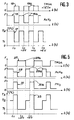
- FIG. 1 relates to the growth of a layer of GaAs, doped or not, by chemical vapor decomposition of TMGa or TEGa, denoted RGa, with arsine AsH3.
- Curves 1 and 3 relate respectively to the supply of gallium and the supply of arsenic on a monocrystalline GaAs substrate, for example of crystal orientation [100].
- Curve 5 corresponding to this temperature modulation, is also in the form of periodic thermal pulses in the form of slots having alternately temperature stages T1 and temperature stages T2, with T2> T1.
- the substrate is brought to temperature T1 when it is introduced into the deposit enclosure the alkyl gallium and the substrate are brought to temperature T2 when the arsenic is introduced into the deposition chamber.
- the gas supplies and the temperature modulation are perfectly synchronized.
- the temperatures T1 and T2 are close to, or even identical to, the decomposition temperatures of RGa and AsH3 respectively on the surface of the substrate.
- the temperature T1 In diffusion mode, that is to say at high temperatures, the temperature T1 is equal to 500 ⁇ 20 ° C and the temperature T2 is equal to 700 ⁇ 20 ° C.
- the temperature T1 For a surface kinetics regime, that is to say at low temperatures, the temperature T1 is equal to 300 ⁇ 20 ° C and the temperature T2 to 500 ⁇ 20 ° C.
- the time of presence of alkyl gallium (RGa) and that of arsine in the deposition enclosure are identical.
- the duration of level T1 is identical to the duration of level T2; the half-period v of the pulses of curve 5 is equal to 1 second, which is the time necessary to deposit a monolayer of undoped GaAs, ie a thickness of the order of 0.3 nm of GaAs, with a gas pressure of 103 Pa.
- stages 1a and 3a The total duration of the gas supply (stages 1a and 3a) necessary for the deposition and therefore that of the heat treatment (stages T1 and T2), are directly proportional to the thickness of the layer of GaAs which it is desired to obtain.
- the deposition of a 30 nm GaAs layer requires a total time of 10 s, which is relatively short.
- the deposition of a layer of III-V material is generally preceded by a step of preparing the surface of the substrate on which the deposition takes place.
- This preparation consists in supplying element V to the surface of the substrate in order to compensate for the gaps in this element on the surface of said substrate.
- the first gas introduced into the deposition enclosure is that of element V and that the substrate is brought to temperature T2.
- the duration of the element V on the surface of the substrate is not critical, it is sufficient that it is greater than 1 s, time necessary to saturate the surface with element V.
- the epitaxial growth proper of the monocrystalline layer of III-V material does not begin that at time to.
- the introduction and removal of the dopant in the deposition enclosure which is generally an element of column II of the periodic table of the elements, is most often carried out simultaneously and in a manner synchronized with the supply respectively the removal of alkyl gallium, as indicated in FIG. 1.
- the main p dopants used are obtained by decomposition of organo-metals and that their decomposition temperature is close to that of the organo-metallic of element III and that the acceptor elements are substitute on the sites of sub-network III.
- p dopant it is possible, for example, to mention the cadmium obtained by decomposition of DMCd.
- the introduction and the suppression of the doping gas in the deposition enclosure are generally carried out simultaneously and in synchronization with those of arsine, as indicated in FIG. 1.
- the dopants generally used (S) are obtained by decomposition of hydrogenated compounds ( H2S) and that their decomposition temperature is close to that of arsine.
- n-GaAs As an alternation to this structure, it is possible to form a layer of n-GaAs in the manner described above. We thus obtain a structure (nipi).
- the temperature and gas supply cycles are an alternation of the cycles described above to form successively p-GaAs / GaAs / n-GaAs layers.
- the curves in FIG. 2 relate to the deposition of a layer of InP, not intentionally doped, by thermal decomposition on the surface of the substrate of trimethylindium or triethylindium (denoted RIn) and of phosphine.
- Curve 7 corresponds to the cycle of introduction and stop of alkylindium and curve 9 corresponds to the cycle of introduction and stop of phosphine.
- these curves 7 and 9 have the form of periodic slots.
- the supply of indium on an orientation InP substrate [100] corresponding to level 7a of curve 7 and the supply of phosphorus corresponding to level 9a of curve 9 are alternated.
- This heat treatment also takes the form of a series of periodic thermal pulses in the form of slots having alternately stages at temperature T1 and stages 4 at temperature T2 with T1 ⁇ T2, the substrate being brought to temperature T1 during the supply of alkylindium and to temperature T2 during the supply of phosphine.
- the contributions in chemical species and the temperature modulation are perfectly synchronized, as before.
- the duration of the thermal pulses v equal to that of the indium and phosphorus inputs, is between 1 and 10 s in order to obtain an InP monolayer of 0.3 nm thick with a gas pressure of 103 Pa.
- T1 is equal to 400 ⁇ 20 ° C and T2 to 800 ⁇ 20 ° C, which corresponds to the decomposition temperatures of TMIn and PH3 respectively on the surface of the substrate.
- H2S is introduced at the same time as phosphine and MCd at the same time as alkylindium.
- FIG. 3 corresponds to the growth of a ternary layer of the Ga x In 1-x As type obtained by thermal decomposition of trimethylgallium, trimethylindium and arsine at the surface of the substrate.
- the growth cycle of these compounds is identical to that of GaAs illustrated in FIG. 1 with the exception of the supply of triethylindium on a substrate in orientation AsAs or GaAs [100], at the same time as the supply of trimethylgallium.
- curve 13 corresponds to the simultaneous cycles of trimethylgallium and trimethylindium
- curve 15 to the arsine cycle
- curve 17 gives the corresponding temperature modulation.
- the III-V substrate is brought to the temperature T1 ⁇ T2 during the supply of gallium and indium, represented by the level 13a of the curve 13, and successively at the temperature T2, during the supply of arsine, corresponding to stage 15a of curve 15.
- the duration of the thermal pulses and of the deposition gas supply v varies from 1 to 10 s in order to obtain a Ga x In 1-x As monolayer 0.3 nm thick.
- the value of the index x is fixed by the partial pressures of TMGa and TEIn prevailing in the deposit enclosure.
- n or p doping of these ternary materials is carried out, as described with reference to FIG. 1, the supply of n dopant being carried out simultaneously with that of ASH3 and the supply of p dopant being carried out simultaneously with those of TMGa and TIN.
- phosphine can partially decompose between 700 and 800 ° C, it is possible to choose the phosphorus composition of compounds of the GaInP type as a function of the temperature of heating of the substrate, temperature corresponding to the level T2 of the pulse heat treatment.
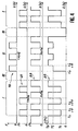
- curves shown in FIG. 4 correspond to the epitaxial growth of a pseudo-alloy or of alternating layers of GaAs / AlAs from the thermal decomposition of TMGa, TMAl and arsine.
- Curves 19, 21 and 23 correspond respectively to the supply of TMAl, TMGa and arsine on a GaAs or AlAs orientation substrate [100].
- Curve 25 represents the temperature modulation associated with this growth gas modulation. Parts I of FIG. 4 correspond to the deposition of GaAs and parts II correspond to the deposition of AlAs.
- the deposition of GaAs is done as described with reference to FIG. 1, the supplies of TMGa and of arsine on the substrate being alternated, the supply of arsine taking place at the temperature T2 and the supply of TMGa at the temperature T1 with T2> T1 close to 500 and 700 ⁇ 20 ° C respectively in diffusion regime.
- the TMAl and arsine intakes are alternated.
- the temperature of the substrate is maintained at the temperature T2 for decomposition of arsine on the surface of the substrate during the supply of arsine and the substrate is maintained at the temperature T′1, close to the decomposition temperature of TMAl at the surface of the substrate during the supply of TMAl.
- TMAl requiring thermal decomposition temperatures as high as those of arsine, and this to avoid the incorporation of oxygen in the semiconductor layer, it is possible to choose T′1 identical to T2 and close to 700 ° C under diffusion regime.
- the GaAs deposition cycle and then that of AlAs are repeated as many times as necessary depending on the thickness of the pseudo-alloy layer that it is desired to obtain.
- the ratio of the durations of parts I and II fixes the average composition of the pseudo-alloy.
- the temperature of the substrate is brought back to ambient temperature.
- the gas change to allow the deposition of AlAs respectively GaAs is carried out during the period III of cooling of the substrate, the duration of which is approximately 15 s.
- n or p doping of this pseudo-alloy is in particular carried out under the same conditions as those described with reference to FIG. 1.
- FIG. 5 relates to the deposition of ternary layers of the GaAs x P 1-x type with 0 ⁇ x ⁇ 1 by thermal decomposition of TMGa, arsine and phosphine.
- TMGa thermal decomposition of the GaAs x P 1-x type with 0 ⁇ x ⁇ 1 by thermal decomposition of TMGa, arsine and phosphine.
- the difficulty comes from the fact that the arsine and the phosphine which should be introduced simultaneously into the enclosure, in alternation with the introduction of TMGa, require different decomposition temperatures in order to remain in yields of reasonable cracking.
- the cycle of incorporation of the element V of the layer to be deposited is broken down into two parts, a high temperature part with the addition of phosphine and a low temperature part with the addition of arsine.
- Curve 33 represents the temperature modulation of the corresponding substrate.
- the supply of gallium (level 27a) is carried out while the substrate is maintained at the lowest temperature T1 and the supply of elements V is carried out while the substrate is maintained at a temperature, above T1.
- the supply of arsine on the substrate III-V, represented by the bearings 29a of the curve 29 is carried out while the substrate is maintained at the temperature T2 and the supply of phosphine, symbolized by the bearings 31a of curve 31, is carried out while the substrate is maintained at a temperature T3 greater than T2.
- the temperature T1 is equal to 500 ⁇ 20 ° C
- the temperature T2 is equal to 700 ⁇ 20 ° C
- the temperature T3 is equal to 800 ⁇ 20 ° C.
- the duration of the level T1 is equal to the duration of the levels T2 + T3 and to the duration of the contributions of gallium and V elements respectively.
- the partial pressure of arsine can be canceled or maintained at a value lower than that necessary to allow the chemical reactions leading to the deposition of GaAs.
- the duration of the supply of gallium and that of the elements V is close to 1 s and the gas pressure is 103 Pa to obtain a 0.3 nm GaAsP monolayer.
- the respective duration of the stages 29a and 31a and therefore of the temperature stages T2 and T3 fixes the composition x of the compound GaAs x P 1-x .
- FIG. 6 shows the growth of a layer of doped or undoped II-VI binary material.
- Curves 34 and 36 relate respectively to the supply of element II and to the supply of element VI on a monocrystalline substrate in II-VI, III-V or IV, for example of crystal orientation [100]. These curves are still presented in the form of a series of periodic pulses in the form of slots.
- the bearings 34a correspond to the supply of dimethylcadmium or diethylcadmium (denoted RCd) of the deposit enclosure.
- the gases introduced during the bearings 34a are dimethylzinc or diethylzinc (RZn).
- the bearings 36a correspond to the supply of H2S or H2Se or ethyltellide to the deposition enclosure depending on whether the element VI of the layer must be sulfur, selenium or tellurium.
- the bearings 34a and 36a are alternated.
- Curve 37 is also in the form of periodic thermal pulses in the form of slots having alternately temperature stages T1 and temperature stages T2 with T2> T1.
- the substrate is brought to the temperature T1 when the gas having to supply, by thermal decomposition on the substrate, the element II and the substrate is brought to temperature T2 when the gas having to supply, by thermal decomposition on the substrate, the element to be brought to temperature T2 VI.
- the gas supplies and the temperature modulation are perfectly synchronized.
- the temperatures T1 and T2 are optimized to have the best decomposition yields for the different gases used.
- the temperature ranges used are:
- the presence times of the gases in the enclosure are identical.
- the duration of the level T1 is identical to the duration of the level T2.
- the half-period v of the pulses of curve 37 is equal to 1 s, which is the time necessary to deposit an undoped II-VI monolayer, ie a thickness of the order of 0.3 nm with a partial pressure of the active gas in the range of 10 to 103 Pa.
- stages 34a and 36a The total duration of the gas supply (stages 34a and 36a) necessary for the deposition and therefore that of the heat treatment (stages T1 and T2) are directly proportional to the thickness of the layer of II-VI which it is desired to obtain .
- the deposition of a layer of II-VI material is generally preceded by a step of preparing the surface of the substrate on which the deposition takes place.
- This preparation consists of a supply of element VI to the surface of the substrate. It is for this reason that the first gas introduced into the deposition enclosure is that of element VI and that we begin by bringing the substrate to temperature T2.
- the duration of this step is not critical. It is enough that it is greater than the second for the partial pressures of gas indicated above.
- these doping elements are obtained by thermal decomposition of their polyalkyls or their hydrides.
- composts providing element III are introduced at the same time as those giving element II during the stages 34a indicated in FIG. 6, or the compounds providing element VII at the same time as those giving element VI during the stages 36a indicated in FIG. 6, all of this without changing anything at the temperature cycle indicated by curve 37.
- TMIn is introduced in the same cycle as RZn, or HCl in the H2Se cycle.
- the proportions of the partial pressures of these gases are related to the desired doping level.
- either the compounds providing element I are introduced at the same time as those releasing element II, that is to say during the stages 34a of FIG. 6, or the compounds providing the element V at the same time as those releasing the element VI, that is to say during the bearings 36a of FIG. 6.
- NH3 or AsH3 or PH3 is introduced at the same time as H2Se, in the proportions of partial pressures desired for the level of doping sought, without changing anything in the cycle thermal indicated by curve 37 in Figure 6.
- III-V layers it is possible to produce a stack of II-VI layers of the same composition AB but doped differently. For this, it suffices to carry out gas input and temperature modulation cycles of the substrate in relation to the layer thicknesses and the doping alternations. We can thus obtain structures np, ni, pi, nipi, etc.
- the substrate is brought to temperature T1 ⁇ T2 during the supply of Cd and Hg and successively to temperature T2 during the supply of Te.
- the duration of the thermal pulses and of the supply of deposition gas v varies from 1 to 10 s in order to obtain a monolayer of Cd x Hg 1-x Te of the order of 0.3 nm thick.
- the value of the index x is fixed by the ratio of the partial pressures of DMCd and of the vapors of Hg prevailing in the deposit enclosure.
- n or p doping of these ternary II-VI layers is carried out as described above for the binary II-VI layers with reference to FIG. 6.
- T′1 and T2 are respectively close to 390 ° C and 450 ° C.
- the temperature of the substrate is maintained at the temperature T2 for decomposing DETe during the supply of DETe and the substrate is maintained at the temperature T1 which may be between T′1 and ambient temperature, during the supply of vapors.
- the HgTe deposition cycle and then that of CdTe are repeated as many times as necessary depending on the thickness of the layer of pseudo-alloy that it is desired to obtain.
- the ratio of the durations of parts I and II fixes the average composition of the pseudo-alloy.
- n or p doping of this pseudo-alloy is in particular carried out under the same conditions as those described with reference to FIG. 6.
- Ternary layers of the Zn Se x S 1-x type with 0 ⁇ x ⁇ 1 and two types of elements VI can be produced by a cycle identical to that described in FIG. 3.
- the bearings 13a then correspond to the introduction of RZn.
- the bearings 15a correspond to the simultaneous introduction of H2S and H2Se.
- the substrate is brought to temperature T1 ⁇ T2 during the introduction of RZn and successively to temperature T2 during the introduction of H2S and H2Se.
- Pulse duration and the deposition gas supply v varies from 1 to 10 s in order to obtain a monolayer of ZnSe x S 1-x of the order of 0.3 nm thick.
- the value of the index x is fixed by the ratio of the partial pressures of H2Se and H2S prevailing in the deposit enclosure during the plateau 15a.
- the temperature T1 can be chosen between 350 ° C and 450 ° C and T2 between 500 ° C and 600 ° C.
- the H2S is introduced simultaneously with the H2Se (during the stages 15a), the substrate is maintained at a temperature T2 close to 600 ° C throughout the duration of the supply of elements VI.
- the ratio of the partial pressures of H2S and H2Se during the stages 15a defines the value of x.
- the deposition of ternary layers of the CdSe x Te 1-x type with 0 ⁇ x ⁇ 1 by thermal decomposition of DMCd, H2Se and DETe can be carried out according to the cycle described in FIG. 5.
- the cycle of incorporation of the elements VI of the layer to be deposited is broken down into two parts, a high temperature part during the introduction of H2Se and a low temperature part during the introduction of DETe.
- Curve 33 represents the temperature modulation of the corresponding substrate.
- the supply of Cd (steps 27a) is carried out while the substrate is maintained at the lowest temperature T1 and the supply of elements VI is carried out while the substrate is maintained at a temperature above T1.
- the supply of DETe (stages 29a) is carried out while the substrate is maintained at temperature T2 and the supply of H2Se (stages 31a) is carried out while the substrate is maintained at a temperature T3 greater than T2 .
- the temperature T1 can be equal to 400 ° ⁇ 20 ° C
- the temperature T2 can be equal to 450 ° ⁇ 20 ° C
- the temperature T3 can be equal to 600 ° ⁇ 50 ° C
- the duration of stage T1 is still equal to the sum of the durations of stages T2 and T3.
- the partial pressure of H2Se can be canceled or maintained at a value lower than that necessary to allow the pyrolysis leading to the release of the element Se.
- the duration of the supply of Cd and that of the supply of elements VI are close to 1 s and the partial pressures of the gases are in the range of 103 Pa to obtain a monolayer of 0.3 nm of CdSe x Te 1- x the ratio of the durations of the stages fixes the composition x of the compound.
- This device with horizontal configuration comprises a vacuum enclosure 50 in which are placed, in a quartz tube, several monocrystalline substrates 52 of III-V or II-VI material on which it is desired to deposit a semiconductor layer according to the invention.
- the sample carriers must have the lowest possible thermal inertia and not be in contact with the substrates in order to allow temperature modulation to control deposits to the nearest monolayer.
- the gases necessary for the epitaxial growth of the semiconductor layers are introduced at one of the ends 54 of the enclosure 50, the other end being used for the evacuation of the reaction gases (CH4, C2H 6 in particular), unreacted gas and possibly for vacuuming the enclosure 50.
- the reaction gases CH4, C2H 6 in particular
- Line 56a is used for example for the introduction of arsine or ammonia; line 56b is used for the introduction of a neutral gas such as a rare gas or nitrogen in order to purge the entire device between each change of gas; the supply line 56c is used for example for the introduction of phosphine, of H2S or HX (X being a halogen); the supply line 56d is used for the introduction of organometallic gases of the RM type where R represents the trimethyl, triethyl or diethyl radical and M a metal from column III or VI of the periodic table of the elements, and the supply line 56e feed serves for example for the introduction of metallic vapors and in particular of mercury.
- a neutral gas such as a rare gas or nitrogen
- the supply line 56c is used for example for the introduction of phosphine, of H2S or HX (X being a halogen)
- the supply line 56d is used for the introduction of organometallic gases of the RM type where R represents the trimethyl, trieth
- the supply lines 56a-56e of the different gases are equipped with solenoid valves 58 and mass flowmeters 59 serving to regulate and stabilize the gas flow rate of the different gases, these solenoid valves and flowmeters being controlled by an electronic control circuit 60.
- a pressure gauge 62 connected to an electronic reading circuit 64 makes it possible to measure the pressure prevailing inside the enclosure 50. This measurement information is sent to a computer 66 then driving the electronic control circuit 60 of the solenoid valves 58.
- the vacuum enclosure 50 is placed in a halogen lamp oven 68 making it possible to modulate the temperature of the substrates 52, facing the lamps, in accordance with the invention.
- Temperature measurement probes 70 located inside the enclosure 50 make it possible to measure the temperature of the substrates 52.
- the temperature measured is sent via an electronic reading circuit 72 to the computer 66 in order to regulate the heating temperature of the substrates 52 as well as the duration of the thermal pulses.
- the computer 66 is connected to an electronic circuit 74 for controlling and supplying electrical power to the halogen lamps 68.
- the device described above allows automatic regulation of the heating temperatures of the substrates 52 as well as a synchronized gas flow regulation according to the nature of the layers of III-V or II-VI material to be deposited, in accordance with the invention .
- the device for implementing the method according to the invention may have a vertical configuration instead of a horizontal configuration and be fitted with other gas pipes.
- other semiconductor layers of material II-VI or III-V and other gas alternations than those illustrated can be used, in accordance with the method according to the invention.
Landscapes
- Chemical & Material Sciences (AREA)
- Engineering & Computer Science (AREA)
- Materials Engineering (AREA)
- Metallurgy (AREA)
- Organic Chemistry (AREA)
- Crystallography & Structural Chemistry (AREA)
- General Chemical & Material Sciences (AREA)
- Chemical Kinetics & Catalysis (AREA)
- Inorganic Chemistry (AREA)
- Mechanical Engineering (AREA)
Claims (15)
Applications Claiming Priority (2)
| Application Number | Priority Date | Filing Date | Title |
|---|---|---|---|
| FR8710290A FR2618455B1 (fr) | 1987-07-21 | 1987-07-21 | Procede de croissance epitaxiale de couches en materiau iii-v ou ii-vi par modulation rapide de la temperature |
| FR8710290 | 1987-07-21 |
Publications (2)
| Publication Number | Publication Date |
|---|---|
| EP0300904A1 EP0300904A1 (de) | 1989-01-25 |
| EP0300904B1 true EP0300904B1 (de) | 1992-01-02 |
Family
ID=9353365
Family Applications (1)
| Application Number | Title | Priority Date | Filing Date |
|---|---|---|---|
| EP19880401883 Expired - Lifetime EP0300904B1 (de) | 1987-07-21 | 1988-07-20 | Verfahren zur Herstellung von Epitaxieschichten aus III-V- oder II-VI-Materialien durch Hochgeschwindigkeitstemperaturmodulation |
Country Status (4)
| Country | Link |
|---|---|
| EP (1) | EP0300904B1 (de) |
| JP (1) | JPS6439719A (de) |
| DE (1) | DE3867352D1 (de) |
| FR (1) | FR2618455B1 (de) |
Families Citing this family (4)
| Publication number | Priority date | Publication date | Assignee | Title |
|---|---|---|---|---|
| JP6055325B2 (ja) * | 2013-01-30 | 2016-12-27 | シャープ株式会社 | 窒化物半導体結晶の製造方法 |
| JP6055290B2 (ja) * | 2012-11-26 | 2016-12-27 | シャープ株式会社 | 窒化物半導体結晶の製造方法 |
| CN113097057A (zh) * | 2021-03-31 | 2021-07-09 | 中国科学院苏州纳米技术与纳米仿生研究所 | 外延生长方法、外延结构及光电器件 |
| CN121575485A (zh) * | 2026-01-28 | 2026-02-27 | 山东华光光电子股份有限公司 | 一种用于提升GaAs外延层均匀性的温度振荡生长方法 |
Family Cites Families (5)
| Publication number | Priority date | Publication date | Assignee | Title |
|---|---|---|---|---|
| US3721583A (en) * | 1970-12-08 | 1973-03-20 | Ibm | Vapor phase epitaxial deposition process for forming superlattice structure |
| US4261771A (en) * | 1979-10-31 | 1981-04-14 | Bell Telephone Laboratories, Incorporated | Method of fabricating periodic monolayer semiconductor structures by molecular beam epitaxy |
| JPS5959876A (ja) * | 1982-09-30 | 1984-04-05 | Ushio Inc | 光照射炉の運転方法 |
| JPH0766910B2 (ja) * | 1984-07-26 | 1995-07-19 | 新技術事業団 | 半導体単結晶成長装置 |
| JPH0766906B2 (ja) * | 1984-07-26 | 1995-07-19 | 新技術事業団 | GaAsエピタキシャル成長方法 |
-
1987
- 1987-07-21 FR FR8710290A patent/FR2618455B1/fr not_active Expired - Fee Related
-
1988
- 1988-07-20 DE DE8888401883T patent/DE3867352D1/de not_active Expired - Lifetime
- 1988-07-20 EP EP19880401883 patent/EP0300904B1/de not_active Expired - Lifetime
- 1988-07-20 JP JP17931188A patent/JPS6439719A/ja active Pending
Also Published As
| Publication number | Publication date |
|---|---|
| FR2618455B1 (fr) | 1994-03-18 |
| FR2618455A1 (fr) | 1989-01-27 |
| JPS6439719A (en) | 1989-02-10 |
| DE3867352D1 (de) | 1992-02-13 |
| EP0300904A1 (de) | 1989-01-25 |
Similar Documents
| Publication | Publication Date | Title |
|---|---|---|
| JP3879173B2 (ja) | 化合物半導体気相成長方法 | |
| EP0477096B1 (de) | Verfahren zum selektiven epitaxialen Wachstum und Ätzen von III-V oder II-VI-Halbleitern in demselben Wachstumsapparat | |
| FR2701599A1 (fr) | Procédé de croissance d'un semiconducteur composite. | |
| JP2008004962A (ja) | Iii−v/ii−vi半導体インターフェイス製造法 | |
| EP0231544B1 (de) | Reaktionskammer für Epitaxiekristallzüchtung aus gasförmiger Phase von Halbleitermaterialien | |
| FR2578680A1 (fr) | Procede pour former une couche mince monocristalline de compose semi-conducteur | |
| EP0300904B1 (de) | Verfahren zur Herstellung von Epitaxieschichten aus III-V- oder II-VI-Materialien durch Hochgeschwindigkeitstemperaturmodulation | |
| Mori et al. | Microstructure and luminescent properties of novel InGaP alloys on relaxed GaAsP substrates | |
| WO1998056091A9 (en) | LONG WAVELENGTH DH, SCH AND MQW LASERS BASED ON Sb | |
| US7575946B2 (en) | Method for making compound semiconductor and method for making semiconductor device | |
| EP0806495B1 (de) | Verfahren zur Beschichtung mittels MOCVD | |
| JP2702889B2 (ja) | 半導体層の結晶成長方法 | |
| JP2686859B2 (ja) | n形のII−VI族化合物半導体を結晶成長する方法 | |
| WO2008009805A1 (fr) | Procede pour la croissance de nitrure d' indium | |
| JP3915750B2 (ja) | 化合物半導体の気相成長方法 | |
| JP2736655B2 (ja) | 化合物半導体結晶成長方法 | |
| WO2020127603A1 (fr) | Substrat semi-conducteur avec couche intermediaire dopee n | |
| WO2020127605A1 (fr) | SUBSTRAT SEMI-CONDUCTEUR CO-DOPE n | |
| JPS6317293A (ja) | 化合物半導体薄膜形成法 | |
| JPS63288027A (ja) | 2−6属化合物半導体薄膜の成長方法 | |
| Vincenzini | High Performance Ceramic Films and Coatings | |
| Bour | Organometallic Vapor Phase Epitaxial Growth and Characterization of Aluminum-gallium-indium-phosphide for Visible Emitters | |
| FR2675948A1 (fr) | Materiaux semi-conducteurs a structure heteroepitaxiee et contrainte controlee, leur mode d'elaboration et leurs applications. | |
| DenBaars | Light emitting diodes: materials growth and properties | |
| HK40102790A (zh) | 掩埋活化p-(al,in)gan层 |
Legal Events
| Date | Code | Title | Description |
|---|---|---|---|
| PUAI | Public reference made under article 153(3) epc to a published international application that has entered the european phase |
Free format text: ORIGINAL CODE: 0009012 |
|
| AK | Designated contracting states |
Kind code of ref document: A1 Designated state(s): DE GB |
|
| 17P | Request for examination filed |
Effective date: 19890628 |
|
| 17Q | First examination report despatched |
Effective date: 19910116 |
|
| GRAA | (expected) grant |
Free format text: ORIGINAL CODE: 0009210 |
|
| AK | Designated contracting states |
Kind code of ref document: B1 Designated state(s): DE GB |
|
| REF | Corresponds to: |
Ref document number: 3867352 Country of ref document: DE Date of ref document: 19920213 |
|
| GBT | Gb: translation of ep patent filed (gb section 77(6)(a)/1977) | ||
| PLBE | No opposition filed within time limit |
Free format text: ORIGINAL CODE: 0009261 |
|
| STAA | Information on the status of an ep patent application or granted ep patent |
Free format text: STATUS: NO OPPOSITION FILED WITHIN TIME LIMIT |
|
| 26N | No opposition filed | ||
| PGFP | Annual fee paid to national office [announced via postgrant information from national office to epo] |
Ref country code: GB Payment date: 19960711 Year of fee payment: 9 |
|
| PGFP | Annual fee paid to national office [announced via postgrant information from national office to epo] |
Ref country code: DE Payment date: 19960717 Year of fee payment: 9 |
|
| PG25 | Lapsed in a contracting state [announced via postgrant information from national office to epo] |
Ref country code: GB Free format text: LAPSE BECAUSE OF NON-PAYMENT OF DUE FEES Effective date: 19970720 |
|
| GBPC | Gb: european patent ceased through non-payment of renewal fee |
Effective date: 19970720 |
|
| PG25 | Lapsed in a contracting state [announced via postgrant information from national office to epo] |
Ref country code: DE Free format text: LAPSE BECAUSE OF NON-PAYMENT OF DUE FEES Effective date: 19980401 |