EP0301483A2 - Dispositif de commande pour convertisseur de puissance - Google Patents
Dispositif de commande pour convertisseur de puissance Download PDFInfo
- Publication number
- EP0301483A2 EP0301483A2 EP88112057A EP88112057A EP0301483A2 EP 0301483 A2 EP0301483 A2 EP 0301483A2 EP 88112057 A EP88112057 A EP 88112057A EP 88112057 A EP88112057 A EP 88112057A EP 0301483 A2 EP0301483 A2 EP 0301483A2
- Authority
- EP
- European Patent Office
- Prior art keywords
- memory
- writing
- abnormal state
- power converter
- control apparatus
- Prior art date
- Legal status (The legal status is an assumption and is not a legal conclusion. Google has not performed a legal analysis and makes no representation as to the accuracy of the status listed.)
- Granted
Links
- 230000015654 memory Effects 0.000 claims abstract description 72
- 230000002159 abnormal effect Effects 0.000 claims abstract description 45
- 238000001514 detection method Methods 0.000 claims description 21
- 239000000872 buffer Substances 0.000 claims description 18
- 230000000694 effects Effects 0.000 abstract 1
- 101100524516 Saccharomyces cerevisiae (strain ATCC 204508 / S288c) RFA2 gene Proteins 0.000 description 10
- 101100033865 Saccharomyces cerevisiae (strain ATCC 204508 / S288c) RFA1 gene Proteins 0.000 description 5
- 125000004122 cyclic group Chemical group 0.000 description 5
- 230000003252 repetitive effect Effects 0.000 description 4
- 239000003990 capacitor Substances 0.000 description 2
- 238000010586 diagram Methods 0.000 description 2
- 238000000034 method Methods 0.000 description 2
- 238000011084 recovery Methods 0.000 description 2
- 230000004044 response Effects 0.000 description 2
- 230000003068 static effect Effects 0.000 description 2
- 230000001360 synchronised effect Effects 0.000 description 2
- 230000015572 biosynthetic process Effects 0.000 description 1
- 238000005070 sampling Methods 0.000 description 1
- 238000003786 synthesis reaction Methods 0.000 description 1
Images



Classifications
-
- H—ELECTRICITY
- H02—GENERATION; CONVERSION OR DISTRIBUTION OF ELECTRIC POWER
- H02M—APPARATUS FOR CONVERSION BETWEEN AC AND AC, BETWEEN AC AND DC, OR BETWEEN DC AND DC, AND FOR USE WITH MAINS OR SIMILAR POWER SUPPLY SYSTEMS; CONVERSION OF DC OR AC INPUT POWER INTO SURGE OUTPUT POWER; CONTROL OR REGULATION THEREOF
- H02M1/00—Details of apparatus for conversion
- H02M1/36—Means for starting or stopping converters
-
- H—ELECTRICITY
- H02—GENERATION; CONVERSION OR DISTRIBUTION OF ELECTRIC POWER
- H02M—APPARATUS FOR CONVERSION BETWEEN AC AND AC, BETWEEN AC AND DC, OR BETWEEN DC AND DC, AND FOR USE WITH MAINS OR SIMILAR POWER SUPPLY SYSTEMS; CONVERSION OF DC OR AC INPUT POWER INTO SURGE OUTPUT POWER; CONTROL OR REGULATION THEREOF
- H02M7/00—Conversion of AC power input into DC power output; Conversion of DC power input into AC power output
- H02M7/42—Conversion of DC power input into AC power output without possibility of reversal
- H02M7/44—Conversion of DC power input into AC power output without possibility of reversal by static converters
- H02M7/48—Conversion of DC power input into AC power output without possibility of reversal by static converters using discharge tubes with control electrode or semiconductor devices with control electrode
- H02M7/53—Conversion of DC power input into AC power output without possibility of reversal by static converters using discharge tubes with control electrode or semiconductor devices with control electrode using devices of a triode or transistor type requiring continuous application of a control signal
- H02M7/537—Conversion of DC power input into AC power output without possibility of reversal by static converters using discharge tubes with control electrode or semiconductor devices with control electrode using devices of a triode or transistor type requiring continuous application of a control signal using semiconductor devices only, e.g. single switched pulse inverters
- H02M7/5387—Conversion of DC power input into AC power output without possibility of reversal by static converters using discharge tubes with control electrode or semiconductor devices with control electrode using devices of a triode or transistor type requiring continuous application of a control signal using semiconductor devices only, e.g. single switched pulse inverters in a bridge configuration
- H02M7/53871—Conversion of DC power input into AC power output without possibility of reversal by static converters using discharge tubes with control electrode or semiconductor devices with control electrode using devices of a triode or transistor type requiring continuous application of a control signal using semiconductor devices only, e.g. single switched pulse inverters in a bridge configuration with automatic control of output voltage or current
-
- H—ELECTRICITY
- H02—GENERATION; CONVERSION OR DISTRIBUTION OF ELECTRIC POWER
- H02M—APPARATUS FOR CONVERSION BETWEEN AC AND AC, BETWEEN AC AND DC, OR BETWEEN DC AND DC, AND FOR USE WITH MAINS OR SIMILAR POWER SUPPLY SYSTEMS; CONVERSION OF DC OR AC INPUT POWER INTO SURGE OUTPUT POWER; CONTROL OR REGULATION THEREOF
- H02M7/00—Conversion of AC power input into DC power output; Conversion of DC power input into AC power output
- H02M7/42—Conversion of DC power input into AC power output without possibility of reversal
- H02M7/44—Conversion of DC power input into AC power output without possibility of reversal by static converters
- H02M7/48—Conversion of DC power input into AC power output without possibility of reversal by static converters using discharge tubes with control electrode or semiconductor devices with control electrode
Definitions
- This invention relates to a control apparatus for a power converter, and more particularly to an apparatus for controlling a power converter, e.g., a PWM inverter for an uninterruptible power supply, a static var compensator, an active filter, etc. by making use of learning control.
- a power converter e.g., a PWM inverter for an uninterruptible power supply, a static var compensator, an active filter, etc. by making use of learning control.
- a first object of this invention is to provide a control apparatus for a power converter which is capable of providing a stable output immediately after an abnormal state ends even if a temporary abnormal state occurs in the power converter.
- a second object of this invention is to provide a control apparatus for a power converter wherein even in the case that a time delay exists from the occurrence an abnormal state to the detection of the event, this control apparatus is capable of eliminating an influence of such a time delay to provide a stable output immediately after the abnormal condition is removed.
- a control apparatus for a power converter comprises a memory capable of storing variables of the power converter over a fixed time period, means for controlling the power converter on the basis of values of the variables stored in the memory, abnormal state detection means for detecting an abnormal state of the power converter, and writing control means that sequentially updates the contents of the memory by writing a newest variable into the memory when the abnormal state detection means does not detect an abnormal state, stops writing into the memory when the abnormal state detection means detects an abnormal state, and restarts writing into the memory when the power converter returns to a normal state or is expected to return to a normal state.
- a control apparatus for a power converter comprises first and second memories capable of storing variables of the power converter over a fixed time period, means for controlling the power converter on the basis of values of the variables stored in the first memory, abnormal state detection means for detecting an abnormal state of the power converter, and writing control means that sequentially updates the contents of the memories by writing a newest variable into the first memory and writing the variable stored in the first memory at a corresponding location of the second memory when the abnormal state detection means does not detect an abnormal state, stops writing into the first memory and replaces variables wrritten in the first memory immediately before stopping writing with variables stored in the corresponding location of the second memory when the abnormal state detection means detects an abnormal state, and restarts writing into the first and second memories when the power converter returns to a normal state or is expected to return to a normal state.
- Fig. 1 shows a triangular wave PWM controlled inverter and a control apparatus therefor.
- a PWM controlled inverter 4 that converts d.c. power from a d.c. power supply 2 to a.c. power, a load 8 is connected through a filter 6 comprising a reactor and a capacitor. It is assumed that the inverter 4 is composed of transistors as an example.
- a potential transformer 10 for detecting an output voltage of the inverter 4 obtained through the filter 6 is provided.
- a current transformer 12 for detecting an output current is provided.
- the inverter 4 is controlled so that an output voltage detected by the potential transformer 10 becomes equal to a reference voltage given by a reference voltage generator 14.
- a voltage deviation or error between a reference voltage from the reference voltage generator 14 and a voltage detected from the potential transformer 10 is obtained by a subtracter 16.
- a controller 18 outputs a modulation signal SW to make the voltage deviation to be zero.
- the controller 18 is constituted as a repetitive control type.
- a memory 26 for a learning control is provided in association with the controller 18.
- a pulse generator 22 On the basis of a modulation signal SW from the controller 18 and a carrier signal TW from a carrier generator 20, a pulse generator 22 generates on control signals. These on control signals are amplified by a pulse amplifier 24. The signals thus amplified are delivered to the inverter 4 to drive transistors constituting the inverter 4.
- the inverter 4 is comprised of four transistor switches A+, A ⁇ , B+ and B ⁇ and the voltage of the d.c. power supply is E volts.
- the pulse generator 22 forms a pair of modulation signals SWA and SWB opposite to each other in phase on the basis of the modulation signal SW (Fig. 3(a)). Then, the pulse generator 22 output on control signals for driving transistor switches A+, A ⁇ , B+ and B ⁇ on the basis of the modulation signals SWA and SWB and a triangular wave carrier TW (Fig. 3(a)) delivered from the carrier generator 20 (Figs.
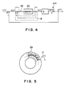
- the controller 18 is constituted as a repetitive control type controller and the control system thereof including memory 26 can be expressed as shown in Fig. 4.
- y p (t) is an output when disturbance of the controlled system G is not taken into consideration
- r(t) is a cyclic reference signal (corresponding to reference voltage)
- e(t) is a control deviation
- d(t) is a cyclic disturbance (corresponding to change in load)
- y(t) is an output of the controlled system when cyclic disturbance d(t) is taken into account.
- a part encompassed by dotted lines corresponds to the controller 18 shown with its gain being omitted.
- the memory 26 has a memory area corresponding to one period based on the output frequency of the inverter 4.
- a switch 28 inserted into the input circuit is closed, thus the contents of the memory 26 is sequentially updated by storing the output variable of the controller.
- control input u(t) of a present cycle can be determined on the basis of data one cycle immediately before the present cycle.
- the switch 28 is opened when an abnormal state, e.g., overload or overvoltage, or the like is detected.
- an abnormal state e.g., overload or overvoltage, or the like
- means for overcurrent detection is shown as one example of abnormal state detection.
- An output current of the inverter 4 detected by the current transformer 12 is compared with an overcurrent detection level set by an overcurrent detection level setter 32. When it exceeds the over current detection level, an overcurrent detection signal is output to a switch control logic 34.
- the switch control logic 34 opens the switch 28 on the basis of the overcurrent detection signal.
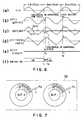
- FIG. 5 An example of the memory 26 is shown in Fig. 5.
- This memory is constituted as a ring buffer.
- f e.g., 50 Hz
- f ⁇ n the frequency of PWM inverter
- this ring buffer includes an n number of memory elements M0, M1, ...., M n-1 .
- a pointer P is moving around the ring buffer at a speed synchronous with the phase rotation of the inverter output voltage. Thus, the content of a memory element indicated by the pointer P is read. Only when the switch 28 is closed, a variable of the controller 18 is written into a memory element indicated by the pointer P.
- the controller 18 computes a modulation signal SW corresponding to the error voltage.
- the pulse generator 22 generates a pulse signal for allowing the transistors constituting the inverter 4 to be in on state on the basis of the modulation signal SW and the carrier signal TW from the carrier generator 20.
- This pulse signal is amplified by the pulse amplifier 24 and is then applied to the PWM inverter 4.
- the a.c. power produced thereby is delivered to the load 8.
- An output voltage of the inverter 4 is detected by the potential transformer 10. The output voltage thus detected is fed back to the subtracter 16. Accordingly, an error between the reference voltage from the reference voltage generator 14 and the voltage detected by the potential transformer 10 is input to the controller 18.
- the controller 18 outputs a modulation signal SW such that the error is equal to zero by making a reference to data of the memory 26 as well.
- the output voltage of the inverter 4 can be in correspondence with the reference voltage ("1st cycle" in Fig. 6).
- Fig. 7 shows a memory 36 of a second embodiment in which the fact mentioned above is taken into account.
- This memory 36 is comprised of two ring buffers BUF1 and BUF2. Both the ring buffers BUF1 and BUF2 are provided with pointers P1 and P2 rotating at a speed synchronous with the phase rotation of the inverter output voltage, respectively.
- This memory 36 is used instead of memory 26 (Fig. 5).
- the switch 28 is closed.
- writing a variable of the controller 18 into the ring buffer BUF1 is conducted.
- the content of a memory element indicated by the pointer P1 of the ring buffer BUF1 is delivered to the controller 18, and at the same time its content is written into a memory element indicated by the pointer P2 of the ring buffer BUF2. Accordingly, in a normal condition, data one cycle before the presently indicated data of the ring buffer BUF1 is written into the ring buffer BUF2.
- the switch control logic 34 writes data written into the ring buffer BUF2 one cycle before, i.e., data from time t0-T which is one cycle earlier than the time at which overload has occurred to time t1-T which is one cycle earlier than the time t1 at which writing into the ring buffer BUF1 is stopped, into corresponding memory elements of the ring buffer BUF1.
- data in a normal state will be revived into the ring buffer BUF1.
- this embodiment can carry out more stable control as compared to that in the first-mentioned embodiment.
- comparator 30 may be used as comparator 30 to cope with overvoltage or undervoltage.
- this invention may be applicable to other power converters, e.g., static var compensator, active filter, and the like, in addition to uninterruptible power supply with PWM inverter control.
Landscapes
- Engineering & Computer Science (AREA)
- Power Engineering (AREA)
- Inverter Devices (AREA)
- Safety Devices In Control Systems (AREA)
- Control Of Electrical Variables (AREA)
- Power Conversion In General (AREA)
Applications Claiming Priority (2)
| Application Number | Priority Date | Filing Date | Title |
|---|---|---|---|
| JP187425/87 | 1987-07-27 | ||
| JP62187425A JPS6434180A (en) | 1987-07-27 | 1987-07-27 | Controlling device of power converter |
Publications (3)
| Publication Number | Publication Date |
|---|---|
| EP0301483A2 true EP0301483A2 (fr) | 1989-02-01 |
| EP0301483A3 EP0301483A3 (en) | 1989-11-15 |
| EP0301483B1 EP0301483B1 (fr) | 1994-03-09 |
Family
ID=16205826
Family Applications (1)
| Application Number | Title | Priority Date | Filing Date |
|---|---|---|---|
| EP88112057A Expired - Lifetime EP0301483B1 (fr) | 1987-07-27 | 1988-07-26 | Dispositif de commande pour convertisseur de puissance |
Country Status (6)
| Country | Link |
|---|---|
| US (1) | US4827392A (fr) |
| EP (1) | EP0301483B1 (fr) |
| JP (1) | JPS6434180A (fr) |
| KR (1) | KR910002352B1 (fr) |
| CA (1) | CA1311550C (fr) |
| DE (1) | DE3888256T2 (fr) |
Cited By (5)
| Publication number | Priority date | Publication date | Assignee | Title |
|---|---|---|---|---|
| WO1993009585A1 (fr) * | 1991-11-04 | 1993-05-13 | Asea Brown Boveri Ab | Reduction des perturbations dans un reseau d'alimentation |
| WO1993009586A1 (fr) * | 1991-11-04 | 1993-05-13 | Asea Brown Boveri Ab | Reduction des perturbations dans un reseau d'alimentation |
| EP0606089A1 (fr) * | 1993-01-07 | 1994-07-13 | Mitsubishi Denki Kabushiki Kaisha | Appareil pour contrôler un convertisseur de puissance |
| EP0768749A3 (fr) * | 1995-10-16 | 1999-09-01 | Sharp Kabushiki Kaisha | Méthode et dipositif de contrÔle d'un onduleur avec suppression de delai dans la boucle de rétroaction |
| WO2001003299A1 (fr) * | 1999-07-01 | 2001-01-11 | Semelab Plc | Amplificateurs d'onde triangulaire et amplificateurs de puissance ameliores |
Families Citing this family (7)
| Publication number | Priority date | Publication date | Assignee | Title |
|---|---|---|---|---|
| SE467130B (sv) * | 1990-09-14 | 1992-05-25 | Electrolux Ab | Kraftaggregat foer generering av en i huvudsak sinusformad utspaenning |
| US5172009A (en) * | 1991-02-25 | 1992-12-15 | Regents Of The University Of Minnesota | Standby power supply with load-current harmonics neutralizer |
| US5483167A (en) * | 1992-09-08 | 1996-01-09 | Mitsubishi Denki Kabushiki Kaisha | Computer controlled ground detecting method for inverter unit and apparatus therefor |
| US5847950A (en) * | 1997-02-19 | 1998-12-08 | Electronic Measurements, Inc. | Control system for a power supply |
| US20100182149A1 (en) * | 2004-05-18 | 2010-07-22 | Marino Ronald A | Apparatus for and method of using rfid antenna configurations |
| US8324861B2 (en) * | 2009-03-05 | 2012-12-04 | O2Micro Inc. | Multi-channel converter with self-diagnosis functionality |
| JP7036270B1 (ja) * | 2021-09-03 | 2022-03-15 | 富士電機株式会社 | 電力変換装置および誘導炉用電力変換装置 |
Family Cites Families (6)
| Publication number | Priority date | Publication date | Assignee | Title |
|---|---|---|---|---|
| US4371824A (en) * | 1979-07-05 | 1983-02-01 | Eaton Corporation | Base drive and overlap protection circuit |
| US4458194A (en) * | 1981-11-04 | 1984-07-03 | Eaton Corporation | Method and apparatus for pulse width modulation control of an AC induction motor |
| ES8404580A1 (es) * | 1982-05-07 | 1984-05-01 | Babcock & Wilcox Co | Dispositivo para generar formas de onda trifasicas de impulsos modulados en anchura para controlar motores de induccion. |
| JPS5972991A (ja) * | 1982-10-19 | 1984-04-25 | Fanuc Ltd | モ−タの制御装置 |
| JPS6023268A (ja) * | 1983-07-18 | 1985-02-05 | 三菱電機株式会社 | エレベ−タの速度制御装置 |
| US4719555A (en) * | 1985-12-19 | 1988-01-12 | Hitachi, Ltd. | Electric power control apparatus with first and second fixed time intervals |
-
1987
- 1987-07-27 JP JP62187425A patent/JPS6434180A/ja active Pending
-
1988
- 1988-07-25 US US07/223,628 patent/US4827392A/en not_active Expired - Lifetime
- 1988-07-25 KR KR1019880009309A patent/KR910002352B1/ko not_active Expired
- 1988-07-26 DE DE3888256T patent/DE3888256T2/de not_active Expired - Lifetime
- 1988-07-26 EP EP88112057A patent/EP0301483B1/fr not_active Expired - Lifetime
- 1988-07-26 CA CA000572990A patent/CA1311550C/fr not_active Expired - Lifetime
Cited By (8)
| Publication number | Priority date | Publication date | Assignee | Title |
|---|---|---|---|---|
| WO1993009585A1 (fr) * | 1991-11-04 | 1993-05-13 | Asea Brown Boveri Ab | Reduction des perturbations dans un reseau d'alimentation |
| WO1993009586A1 (fr) * | 1991-11-04 | 1993-05-13 | Asea Brown Boveri Ab | Reduction des perturbations dans un reseau d'alimentation |
| US5296764A (en) * | 1991-11-04 | 1994-03-22 | Asea Brown Boveri Ab | Reduction of disturbances in a power network |
| US5323330A (en) * | 1991-11-04 | 1994-06-21 | Asea Brown Boveri Ab | Reduction of disturbances in a power network |
| EP0606089A1 (fr) * | 1993-01-07 | 1994-07-13 | Mitsubishi Denki Kabushiki Kaisha | Appareil pour contrôler un convertisseur de puissance |
| US5442538A (en) * | 1993-01-07 | 1995-08-15 | Mitsubishi Denki Kabushiki Kaisha | Apparatus for controlling power converter based on output current |
| EP0768749A3 (fr) * | 1995-10-16 | 1999-09-01 | Sharp Kabushiki Kaisha | Méthode et dipositif de contrÔle d'un onduleur avec suppression de delai dans la boucle de rétroaction |
| WO2001003299A1 (fr) * | 1999-07-01 | 2001-01-11 | Semelab Plc | Amplificateurs d'onde triangulaire et amplificateurs de puissance ameliores |
Also Published As
| Publication number | Publication date |
|---|---|
| DE3888256T2 (de) | 1994-09-01 |
| DE3888256D1 (de) | 1994-04-14 |
| US4827392A (en) | 1989-05-02 |
| CA1311550C (fr) | 1992-12-15 |
| KR910002352B1 (ko) | 1991-04-20 |
| KR890003101A (ko) | 1989-04-12 |
| EP0301483A3 (en) | 1989-11-15 |
| EP0301483B1 (fr) | 1994-03-09 |
| JPS6434180A (en) | 1989-02-03 |
Similar Documents
| Publication | Publication Date | Title |
|---|---|---|
| EP0301483B1 (fr) | Dispositif de commande pour convertisseur de puissance | |
| EP0897213B1 (fr) | Surveillance de courant dans une charge inductive commandée par modulation d'impulsion par un étage en pont | |
| KR910009806B1 (ko) | 무효전력보상장치 | |
| US5115386A (en) | Circuit for controlling an electric power supply apparatus, a method therefor and an uninterruptible power supply | |
| EP0330755A2 (fr) | Dispositif de filtrage actif | |
| JPH1042569A (ja) | パルス幅変調変換器の出力制御装置 | |
| US5475292A (en) | Apparatus for restarting inverter for driving synchronous motor after momentary interruption | |
| US6566838B2 (en) | Fully digital control and drive combination IC with on-board DSP for disk mass storage device | |
| US4143315A (en) | Rms transducer and voltage regulating system employing the same | |
| US4141376A (en) | Digital servovalve drive | |
| JPS63129877A (ja) | 回転制御装置 | |
| JPS63148831A (ja) | 静止形無効電力補償装置の制御装置 | |
| KR980012819A (ko) | 회전모터의 절대각위치 산출장치 및 이를 적용한 속도제어장치 | |
| JPH04322161A (ja) | スイッチングレギュレータ制御方式 | |
| KR20020044191A (ko) | 클럭 동기화 장치의 듀티 보정 회로 | |
| SU1700705A2 (ru) | Управл емый вентильный электродвигатель | |
| SU1159141A1 (ru) | Электропривод посто нного тока | |
| JPH03135376A (ja) | 電力供給装置の制御回路及び制御方法並びに電力供給装置 | |
| JPS5828784B2 (ja) | 周波数弁別器 | |
| JP2598383Y2 (ja) | インバ−タ制御装置 | |
| JPS5985512A (ja) | 位置制御装置 | |
| SU1668973A1 (ru) | Стабилизатор переменного напр жени | |
| JPS6268022A (ja) | 無効電力補償装置の制御方法 | |
| SU1707682A2 (ru) | Реле переменного тока | |
| SU1187149A1 (ru) | Устройство дл управлени электроприводом |
Legal Events
| Date | Code | Title | Description |
|---|---|---|---|
| PUAI | Public reference made under article 153(3) epc to a published international application that has entered the european phase |
Free format text: ORIGINAL CODE: 0009012 |
|
| 17P | Request for examination filed |
Effective date: 19880822 |
|
| AK | Designated contracting states |
Kind code of ref document: A2 Designated state(s): DE GB |
|
| RIN1 | Information on inventor provided before grant (corrected) |
Inventor name: MIGUCHI, YASUHIKO |
|
| PUAL | Search report despatched |
Free format text: ORIGINAL CODE: 0009013 |
|
| AK | Designated contracting states |
Kind code of ref document: A3 Designated state(s): DE GB |
|
| 17Q | First examination report despatched |
Effective date: 19910906 |
|
| GRAA | (expected) grant |
Free format text: ORIGINAL CODE: 0009210 |
|
| AK | Designated contracting states |
Kind code of ref document: B1 Designated state(s): DE GB |
|
| REF | Corresponds to: |
Ref document number: 3888256 Country of ref document: DE Date of ref document: 19940414 |
|
| PLBE | No opposition filed within time limit |
Free format text: ORIGINAL CODE: 0009261 |
|
| STAA | Information on the status of an ep patent application or granted ep patent |
Free format text: STATUS: NO OPPOSITION FILED WITHIN TIME LIMIT |
|
| 26N | No opposition filed | ||
| PGFP | Annual fee paid to national office [announced via postgrant information from national office to epo] |
Ref country code: GB Payment date: 19950717 Year of fee payment: 8 |
|
| PG25 | Lapsed in a contracting state [announced via postgrant information from national office to epo] |
Ref country code: GB Effective date: 19960726 |
|
| GBPC | Gb: european patent ceased through non-payment of renewal fee |
Effective date: 19960726 |
|
| PGFP | Annual fee paid to national office [announced via postgrant information from national office to epo] |
Ref country code: DE Payment date: 20070719 Year of fee payment: 20 |