EP0301601A2 - Circuit de verrouillage - Google Patents
Circuit de verrouillage Download PDFInfo
- Publication number
- EP0301601A2 EP0301601A2 EP88112453A EP88112453A EP0301601A2 EP 0301601 A2 EP0301601 A2 EP 0301601A2 EP 88112453 A EP88112453 A EP 88112453A EP 88112453 A EP88112453 A EP 88112453A EP 0301601 A2 EP0301601 A2 EP 0301601A2
- Authority
- EP
- European Patent Office
- Prior art keywords
- circuit
- mos type
- type gate
- clamping
- holding capacitor
- Prior art date
- Legal status (The legal status is an assumption and is not a legal conclusion. Google has not performed a legal analysis and makes no representation as to the accuracy of the status listed.)
- Granted
Links
- 239000003990 capacitor Substances 0.000 claims abstract description 34
- 238000010276 construction Methods 0.000 claims description 6
- 238000010586 diagram Methods 0.000 description 11
- 230000010355 oscillation Effects 0.000 description 5
- 230000004048 modification Effects 0.000 description 4
- 238000012986 modification Methods 0.000 description 4
- 239000004065 semiconductor Substances 0.000 description 2
- 230000003247 decreasing effect Effects 0.000 description 1
- 230000002950 deficient Effects 0.000 description 1
- 230000000977 initiatory effect Effects 0.000 description 1
- 230000035945 sensitivity Effects 0.000 description 1
Images
Classifications
-
- H—ELECTRICITY
- H04—ELECTRIC COMMUNICATION TECHNIQUE
- H04N—PICTORIAL COMMUNICATION, e.g. TELEVISION
- H04N5/00—Details of television systems
- H04N5/14—Picture signal circuitry for video frequency region
- H04N5/16—Circuitry for reinsertion of DC and slowly varying components of signal; Circuitry for preservation of black or white level
- H04N5/18—Circuitry for reinsertion of DC and slowly varying components of signal; Circuitry for preservation of black or white level by means of "clamp" circuit operated by switching circuit
Definitions
- This invention relates to a clamping circuit or a clamper suitable for an image processing.
- a clamping circuit For setting an analog output level to a desired external set voltage as in the case of giving a reference black level to a charge coupled device (CCD) output, a clamping circuit is used.
- an object of this invention is to provide a clamping circuit which can have a small size because of a simple construction, and which can perform a stable operation.
- a clamping circuit comprising: a differential output circuit having an input terminal on one side thereof to which an input signal is applied; two MOS type gate circuits connected in series, an output signal from the differential output circuit to be clamped and a reference voltage which is a clamping target value being applied to gate electrodes of the MOS type gate circuits, respectively; reset means including a holding capacitor connected to the drain side of either of the MOS type gate circuits to discharge charge in the holding capacitor at a time when a clamping operation is initiated; a current source connected to a junction between the MOS type gate circuits; charge current flow control means for accumulating current flowing to the junction in the holding capacitor; and feedback means for feeding back a potential of the holding capacitor to an input terminal on the other side of the differential output circuit.
- the differential output circuit is not required to have high sensitivity, an unstable operation such as oscillation is eliminated.
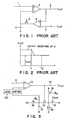
- FIG. 1 showing a typical conventional clamping circuit.
- This circuit includes two differential amplifiers 3 and 4 which are connected in a loop.
- a signal line 1 for transmitting a control signal is connected to the plus (+) side of the differential amplifier 3, and an output of the differential amplifier 4 is connected to the minus (-) side of the differential amplifier 3 through a switch 5 shown as a FET switch, and to a holding capacitor 6.
- An output line 2 of the differential amplifier 3 is connected to the plus (+) side of the differential amplifier 4, and a reference voltage V ref is inputted to the minus (-) side of the differential amplifier 4.
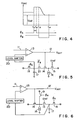
- MOS type gate circuits 14 and 15 are connected in series and a junction therebetween is connected a current source 16.
- An operation completion gate circuit 19 controlled by a pulse ⁇ B is connected to the junction.
- An output line 12 of a differential amplifier 13 is connected to the gate electrode of the MOS type gate circuit 14.
- a reference voltage V ref is applied to the gate electrode of the MOS type gate circuit 15.
- a holding capacitor 17 and a reset gate circuit 18 controlled by a pulse ⁇ A are connected on the drain electrode side of the MOS type gate circuit 14.
- the junction among the reset gate circuit 18, the MOS type gate circuit 14 and the holding capacitor 17 is connected to the plus (+) side input terminal of the differential amplifier 13, acting as an output circuit, through a level shifter 20 for making a level adjustment.
- the MOS type gate circuits 14 and 15 have of substantially the same construction and their characteristics are substantially the same.
- pulse ⁇ A applied to the gate electrode of the reset gate circuit 18 builds up to a high value.
- an electric charge (electrons) in the holding capacitor 17 is discharged, thus bringing the capacitor 17 to a floating state.
- pulse ⁇ B applied to the gate electrode of the operation completion gate circuit 19 is maintained at a high level, e.g., 12 volts.
- the output voltage V out is about 8 volts.
- the pulse ⁇ B builds down.
- the charge in capacitor 17 flows toward the MOS type gate 14 having a potential well deeper than that of the MOS type gate circuit 15, thus allowing its potential well to become shallower.
- the charge also flows into the holding capacitor 17, thus lowering its potential.
- This potential is fed back to the differential amplifier 13 through the level shifter 20.
- V out V ref
- the feedback operation is conducted only when the relation V out > V ref holds. Any feedback operation is not caused under the condition of V out ⁇ V ref , so that any oscillation is not produced.
- V out V ref - ⁇ V.
- FIG. 5 shows a modification of FIG. 3 wherein the charge flowing into the holding capacitor 17 is controlled by the operation completion gate circuit 21 on-off controlled by pulse ⁇ B . Namely, when the operation completion gate circuit 21 is turned on even in a case wherein the potential well directly below the MOS type gate circuit 14 is deeper than the potential well directly below the MOS gate circuit 15, the comparison operation is completed. A clamping value corresponding to the charge in holding capacitor at that time will be outputted.
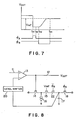
- FIG. 6 is a circuit diagram showing another embodiment of this invention.
- connection relationship of the MOS type gate circuits 14 and 15, the constant current source 16, and the operation completion gate 19 is the same as that in the case shown in FIG. 3.
- This embodiment differs from that shown in FIG. 3 in that MOS type gate circuit 15 having a gate electrode to which a reference voltage is applied and a reset gate circuit 18 are connected in series, and holding capacitor 17 and level shifter 20 connected to the minus (-) side of the output differential amplifier 13 are connected to the junction between gate circuits 15 and 18 and that a control signal is applied to the plus (+) side of the differential amplifier 13.
- FIG. 7 is a waveform diagram showing the clamping operation of the circuit shown in FIG. 6.
- the holding capacitor 17 Before time t21, the holding capacitor 17 is in a charge accumulated state. Since a voltage corresponding to the charge is applied to the minus (-) side of the differential amplifier 13, the output voltage V out is maintained at a potential higher than V ref . During an interval between time t21 and t22, when reset pulse ⁇ A is applied to the reset gate circuit 18, the charge discharges into the drain electrode of gate circuit 14 via gate circuit 15. Thus, the potential of V out is rapidly lowered, resulting in a state where the relation V out ⁇ V ref holds.
- the circuit becomes operative only when the output is lower than V ref .
- the possibility of oscillation, etc. is completely eliminated.
- FIG. 8 is a circuit diagram showing another modification of the embodiment shown in FIG. 6.
- an operation completion gate circuit 22 controlled by pulse ⁇ B is serially inserted between MOS type gate circuits 15 and the holding capacitor 17. Only when the operation completion gate circuit 22 is in an ON state, comparison between an output V out and a reference voltage V ref is made.
- the operation completion gate circuit 22 is required only to control the charge flowing into the holding capacitor 17. For this reason, as shown in Figs. 5 and 8, the operation completion gate circuit 22 can be connected between one of two MOS type gate circuits 14 and 15 and the holding capacitor 17, so that, excellent operation can be performed.
- a reference voltage applied to one of MOS type gate circuits employs a target value as it is in the above-mentioned embodiments
- a voltage expressed as (V ref - ⁇ V) may be used as a reference voltage by taking an error in operation into account, thus making it possible to further improve the clamping accuracy.
Landscapes
- Engineering & Computer Science (AREA)
- Multimedia (AREA)
- Signal Processing (AREA)
- Manipulation Of Pulses (AREA)
- Transforming Light Signals Into Electric Signals (AREA)
- Amplifiers (AREA)
Applications Claiming Priority (2)
| Application Number | Priority Date | Filing Date | Title |
|---|---|---|---|
| JP62192070A JPS6436215A (en) | 1987-07-31 | 1987-07-31 | Clamp circuit |
| JP192070/87 | 1987-07-31 |
Publications (3)
| Publication Number | Publication Date |
|---|---|
| EP0301601A2 true EP0301601A2 (fr) | 1989-02-01 |
| EP0301601A3 EP0301601A3 (en) | 1989-08-09 |
| EP0301601B1 EP0301601B1 (fr) | 1993-03-03 |
Family
ID=16285128
Family Applications (1)
| Application Number | Title | Priority Date | Filing Date |
|---|---|---|---|
| EP88112453A Expired - Lifetime EP0301601B1 (fr) | 1987-07-31 | 1988-08-01 | Circuit de verrouillage |
Country Status (4)
| Country | Link |
|---|---|
| US (1) | US4914324A (fr) |
| EP (1) | EP0301601B1 (fr) |
| JP (1) | JPS6436215A (fr) |
| DE (1) | DE3878773T2 (fr) |
Cited By (3)
| Publication number | Priority date | Publication date | Assignee | Title |
|---|---|---|---|---|
| EP0491186A1 (fr) * | 1990-12-13 | 1992-06-24 | Motorola, Inc. | Circuit de verrouillage |
| US5510854A (en) * | 1993-05-19 | 1996-04-23 | Sgs-Thomson Microelectronics, S.A. | Device for adjusting the black level of a video signal |
| CN108111230A (zh) * | 2018-01-19 | 2018-06-01 | 厦门优迅高速芯片有限公司 | 一种复用光通信光接收组件mon管脚的电路 |
Families Citing this family (7)
| Publication number | Priority date | Publication date | Assignee | Title |
|---|---|---|---|---|
| US5280200A (en) * | 1989-04-10 | 1994-01-18 | Tarng Min M | Pipelined buffer for analog signal and power supply |
| US5390020A (en) * | 1992-09-14 | 1995-02-14 | Eastman Kodak Company | Video amplifier stabilization for CRT printing |
| US5418410A (en) * | 1993-05-25 | 1995-05-23 | Motorola, Inc. | Leading edge blanking circuit |
| US5465067A (en) * | 1994-05-13 | 1995-11-07 | Samsung Semiconductor, Inc. | Current clamping circuit |
| JP3127878B2 (ja) * | 1998-03-18 | 2001-01-29 | 日本電気株式会社 | クランプ回路 |
| US7371609B2 (en) * | 2001-10-26 | 2008-05-13 | Staktek Group L.P. | Stacked module systems and methods |
| CN102792000B (zh) | 2010-04-27 | 2014-11-26 | 三菱重工业株式会社 | 二冲程发动机的扫气通路构造 |
Family Cites Families (5)
| Publication number | Priority date | Publication date | Assignee | Title |
|---|---|---|---|---|
| US3543169A (en) * | 1967-10-30 | 1970-11-24 | Bell Telephone Labor Inc | High speed clamping apparatus employing feedback from sample and hold circuit |
| US4255715A (en) * | 1979-08-27 | 1981-03-10 | Gte Laboratories Incorporated | Offset correction circuit for differential amplifiers |
| US4328434A (en) * | 1979-11-16 | 1982-05-04 | Gte Laboratories Incorporated | Comparator circuit with offset correction |
| US4513321A (en) * | 1982-10-29 | 1985-04-23 | Rca Corporation | Black level clamp for television signals |
| US4742392A (en) * | 1983-08-04 | 1988-05-03 | Canon Kabushiki Kaisha | Clamp circuit with feed back |
-
1987
- 1987-07-31 JP JP62192070A patent/JPS6436215A/ja active Granted
-
1988
- 1988-07-29 US US07/225,816 patent/US4914324A/en not_active Expired - Lifetime
- 1988-08-01 DE DE8888112453T patent/DE3878773T2/de not_active Expired - Fee Related
- 1988-08-01 EP EP88112453A patent/EP0301601B1/fr not_active Expired - Lifetime
Cited By (4)
| Publication number | Priority date | Publication date | Assignee | Title |
|---|---|---|---|---|
| EP0491186A1 (fr) * | 1990-12-13 | 1992-06-24 | Motorola, Inc. | Circuit de verrouillage |
| US5510854A (en) * | 1993-05-19 | 1996-04-23 | Sgs-Thomson Microelectronics, S.A. | Device for adjusting the black level of a video signal |
| CN108111230A (zh) * | 2018-01-19 | 2018-06-01 | 厦门优迅高速芯片有限公司 | 一种复用光通信光接收组件mon管脚的电路 |
| CN108111230B (zh) * | 2018-01-19 | 2023-07-21 | 厦门优迅高速芯片有限公司 | 一种复用光通信光接收组件mon管脚的电路 |
Also Published As
| Publication number | Publication date |
|---|---|
| DE3878773D1 (de) | 1993-04-08 |
| EP0301601B1 (fr) | 1993-03-03 |
| JPH0431602B2 (fr) | 1992-05-27 |
| EP0301601A3 (en) | 1989-08-09 |
| JPS6436215A (en) | 1989-02-07 |
| DE3878773T2 (de) | 1993-08-05 |
| US4914324A (en) | 1990-04-03 |
Similar Documents
| Publication | Publication Date | Title |
|---|---|---|
| US6587144B1 (en) | Analog signal processing apparatus for digital camera | |
| EP0576008B1 (fr) | Circuit de génération de surtension | |
| EP0301601B1 (fr) | Circuit de verrouillage | |
| EP0611059A2 (fr) | Système pour récupérer une composante de courant continu pour les signaux binaires transférés en série | |
| US4812687A (en) | Dual direction integrating delay circuit | |
| US6140878A (en) | Transimpedance-type amplifier circuit with interchangeable resistance | |
| US4835417A (en) | Comparator circuit having improved output characteristics | |
| EP0370814A2 (fr) | Comparateur à verrouillage à suppression de décalage | |
| EP0324456B1 (fr) | Circuit de sortie d'un dispositif de transfert de charge | |
| US4563708A (en) | Method and apparatus for controlling storage time in charge storing photoelectric converter | |
| US5216509A (en) | Sampler hold circuit for CCD image-sensor signal | |
| EP0506081B1 (fr) | Amplificateur de tension et dispositif de prise d'images le comportant | |
| US6600513B1 (en) | Charge transfer device | |
| US4687998A (en) | Pulse width generating circuit synchronized with clock signal and corresponding to a reference voltage | |
| EP0404125B1 (fr) | Circuit élévateur | |
| US4547762A (en) | Digital to analog converting apparatus | |
| US4700085A (en) | Circuit for detecting signal charges transferred in a charge transfer device | |
| US6337887B1 (en) | Burst receiving circuit and control method thereof | |
| US4499386A (en) | Trigger circuit | |
| EP0393996B1 (fr) | Dispositifs à accouplement de charge | |
| US5712475A (en) | Light receiving circuit with variable threshold circuit | |
| EP0311529A2 (fr) | Capteur d'images comportant des régions de stockage de charges | |
| EP0865684A1 (fr) | Circuit de mesure de la charge | |
| JPH02146194A (ja) | サンプルホールド回路 | |
| JP2534717B2 (ja) | クランプ回路 |
Legal Events
| Date | Code | Title | Description |
|---|---|---|---|
| PUAI | Public reference made under article 153(3) epc to a published international application that has entered the european phase |
Free format text: ORIGINAL CODE: 0009012 |
|
| 17P | Request for examination filed |
Effective date: 19880804 |
|
| AK | Designated contracting states |
Kind code of ref document: A2 Designated state(s): DE FR GB |
|
| PUAL | Search report despatched |
Free format text: ORIGINAL CODE: 0009013 |
|
| AK | Designated contracting states |
Kind code of ref document: A3 Designated state(s): DE FR GB |
|
| 17Q | First examination report despatched |
Effective date: 19910726 |
|
| GRAA | (expected) grant |
Free format text: ORIGINAL CODE: 0009210 |
|
| AK | Designated contracting states |
Kind code of ref document: B1 Designated state(s): DE FR GB |
|
| REF | Corresponds to: |
Ref document number: 3878773 Country of ref document: DE Date of ref document: 19930408 |
|
| ET | Fr: translation filed | ||
| PLBE | No opposition filed within time limit |
Free format text: ORIGINAL CODE: 0009261 |
|
| STAA | Information on the status of an ep patent application or granted ep patent |
Free format text: STATUS: NO OPPOSITION FILED WITHIN TIME LIMIT |
|
| 26N | No opposition filed | ||
| PGFP | Annual fee paid to national office [announced via postgrant information from national office to epo] |
Ref country code: GB Payment date: 19970723 Year of fee payment: 10 |
|
| PGFP | Annual fee paid to national office [announced via postgrant information from national office to epo] |
Ref country code: DE Payment date: 19970811 Year of fee payment: 10 |
|
| PG25 | Lapsed in a contracting state [announced via postgrant information from national office to epo] |
Ref country code: GB Free format text: LAPSE BECAUSE OF NON-PAYMENT OF DUE FEES Effective date: 19980801 |
|
| REG | Reference to a national code |
Ref country code: GB Ref legal event code: 746 Effective date: 19981026 |
|
| GBPC | Gb: european patent ceased through non-payment of renewal fee |
Effective date: 19980801 |
|
| REG | Reference to a national code |
Ref country code: FR Ref legal event code: D6 |
|
| PG25 | Lapsed in a contracting state [announced via postgrant information from national office to epo] |
Ref country code: DE Free format text: LAPSE BECAUSE OF NON-PAYMENT OF DUE FEES Effective date: 19990601 |
|
| PGFP | Annual fee paid to national office [announced via postgrant information from national office to epo] |
Ref country code: FR Payment date: 20050809 Year of fee payment: 18 |
|
| REG | Reference to a national code |
Ref country code: FR Ref legal event code: ST Effective date: 20070430 |
|
| PG25 | Lapsed in a contracting state [announced via postgrant information from national office to epo] |
Ref country code: FR Free format text: LAPSE BECAUSE OF NON-PAYMENT OF DUE FEES Effective date: 20060831 |