EP0301616A2 - Digital phase-locked-loop clock extractor for bipolar signals - Google Patents
Digital phase-locked-loop clock extractor for bipolar signals Download PDFInfo
- Publication number
- EP0301616A2 EP0301616A2 EP88201377A EP88201377A EP0301616A2 EP 0301616 A2 EP0301616 A2 EP 0301616A2 EP 88201377 A EP88201377 A EP 88201377A EP 88201377 A EP88201377 A EP 88201377A EP 0301616 A2 EP0301616 A2 EP 0301616A2
- Authority
- EP
- European Patent Office
- Prior art keywords
- signal
- logic
- counter
- frequency
- clock signal
- Prior art date
- Legal status (The legal status is an assumption and is not a legal conclusion. Google has not performed a legal analysis and makes no representation as to the accuracy of the status listed.)
- Granted
Links
Images


Classifications
-
- H—ELECTRICITY
- H04—ELECTRIC COMMUNICATION TECHNIQUE
- H04L—TRANSMISSION OF DIGITAL INFORMATION, e.g. TELEGRAPHIC COMMUNICATION
- H04L7/00—Arrangements for synchronising receiver with transmitter
- H04L7/02—Speed or phase control by the received code signals, the signals containing no special synchronisation information
- H04L7/033—Speed or phase control by the received code signals, the signals containing no special synchronisation information using the transitions of the received signal to control the phase of the synchronising-signal-generating means, e.g. using a phase-locked loop
- H04L7/0331—Speed or phase control by the received code signals, the signals containing no special synchronisation information using the transitions of the received signal to control the phase of the synchronising-signal-generating means, e.g. using a phase-locked loop with a digital phase-locked loop [PLL] processing binary samples, e.g. add/subtract logic for correction of receiver clock
Definitions
- the present invention relates to a digital phase-locked-loop clock extractor for bipolar signals.
- the extractor in accordance with the invention consists of a circuit designed to allow taking from a PCM (pulse code modulation) input signal a clock signal phase locked to the input signal so as to allow sampling of the latter with said clock signal without loss of information even in the presence of jitter (phase distorsion) and frequency tolerance.
- PCM pulse code modulation
- the analog solution uses a tuned circuit or a frequency-controlled oscillator. Maintenance of an appropriate phase between the input signal and the clock signal takes place continuously and the clock signal extracted does not display phase jumps.
- These circuits have been developed by some manufacturers of integrated circuits and can be made as well with discrete components. They display however criticality of operation, the need for calibration and poor reliability.
- the object of the present invention is to develop a clock signal extractor of the digital type which would allow having in normal conditions a low phase jump capable of compensating for the frequency difference between the local clock and the line clock in the presence of low input jitter and at the same time in the presence of high jitter permit sampling of the data signal received without loss of information, producing a higher instantaneous phase correction of the generated clock signal.
- a digital clock extractor for bipolar signals characterized in that it comprises at least one sliding register supplied with a bipolar signal received and sampled with a sampling signal having a frequency which is a multiple of that of said received signal, a transition detector logic associated with a combination of outputs of said register to generate a transition detection signal of the signal received upon reaching a certain sequence of logic states at said register outputs, a frequency divider consisting of a counter fed with said multiple-frequency sampling signal and programmed in such a manner as to give at the output a clock signal extracted at the same frequency as said received signal, said divider having a correction logic which compares said transition detection signal with the momentary logic stage of the outputs of said counter to evaluate the phase error existing between the extracted clock signal and the received signal and command a phase correction of said clock signal the size of which is a progressively increasing function of said error signal.
- the progressively increasing function which is essentially logarithmic, assured between the phase error and the phase correction, acts in such a manner that with a very small phase error, i.e. with the counter essentially in phase with the transition detection signal, no correction is effected. This permits avoiding continuous phase jumps of the clock signal phase locked to the input signal.
- the correction effected permits meeting of the CCITT recommendations without loss of information and to have under normal conditions (with low jitter) an extremely small phase jump.
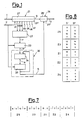
- the digital clock extractor illustrated as an example in FIG. 1 comprises a shift register 21 which receives at its input a 2.948 2Mbit/s bipolar PCM (Pulse Code Modulation) signal sampled with a sampling signal C at 32.768 MHz, i.e. at a frequency 16 times that of the input signal or received data signal I.
- a shift register 21 which receives at its input a 2.948 2Mbit/s bipolar PCM (Pulse Code Modulation) signal sampled with a sampling signal C at 32.768 MHz, i.e. at a frequency 16 times that of the input signal or received data signal I.
- a bipolar PCM signal is known to consist of a sucession of negative and positive return-to-zero pulses.
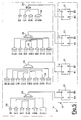
- Appropriate means are therefore provided but not shown in the figure and placed upstream of the register 21 to subdivide the bipolar signal I on two lines in such a manner as to bring the positive pulses I′ onto one of the lines and the negative pulses I ⁇ onto the other with the logic convention that level '0' indicates absence of signal and level "1" indicates presence of the pulse. Said shape of the two signals thus obtained is shown as an example in FIG. 2.
- the shift register 21 is thus made up of a pair of registers 21′-21 ⁇ in parallel, each of which receives the signal (I′, I ⁇ ) present on one of the two lines.
- the shift register 21 has 7 pairs of parallel outputs U1-U7 corresponding to the same number of successive stages of the registers 21′ and 21 ⁇ and of another pair of serial outputs U, one for each register.
- each register 21′, 22 ⁇ comprises auccession of bistable multivibrators 31′, 31 ⁇ which receives at its input a respective signal I′, I ⁇ and supplies a respective serial output U′, U ⁇ corresponding to the output of FIG. 1 and respective parallel outputs U1′-U7′, U1 ⁇ -U7 ⁇ (only the U1′-U3′ and the U1 ⁇ -U3 ⁇ illustrated in FIG. 3) corresponding to the outputs U1-U7 of FIG. 1.
- the input data signal is delayed by 7.5 periods of the sampling signal C, said delay being selected on the basis of the pulse duration of the data signal I received, as an example equal to 244 ns, characteristic of the return-to-zero 2.948 Mbit/s signals.
- this has the purpose of permitting the extracted clock signal to sample the data at the output U of the register 21 during the pulse of said data, preferably in the central part thereof.
- the first three parallel outputs U1, U2 and U3 of the register 21 (i.e. U1′, U2′, U3′; U1 ⁇ , U2 ⁇ , U3 ⁇ of the registers 21′, 21 ⁇ ) are combined in a transition detector logic 22 which through the combination of their logic states obtained through logic gates OR 32 and NAND 33 shown in FIG. 4 detects the presence or absence of a transition of the data received frm 0 to 1 on either one of the two inputs.
- the detector 22 detects the presence of the transition 0--1, which indicates the instant of beginning of the data received by decodification of the 011 sequence at the outputs U3, U2, U1 of the register 21′ o 21 ⁇ . This allows filtering of any spikes present in the input signal I which with the sequence 010 do not produce recognition of the beginning of the data.
- the output of the detector 22 then consists of the logic OR function, carried out by NAND gate 33, of the two decoding logics related to the registers 21′ and 21 ⁇ .
- the transition detection signal T generated by the detector 22 is applied, as a delayed transition detector signal T′, to an input of a combinatory logic 24 which fulfills the functions of phase correction and frequency division of a programmable frequency divider 30.
- the output of the combinatory logic 24 is applied to the input of a register 25 clocked with the sampling signal C, said register constituting the sequential part of the divider 30. All the outputs of the register 25 are brought back to other inputs of the combinatory logic 24 while the most significant output of the register constitutes the extracted clock signal S having the same frequency as the received signal I.
- Said clock signal is used for example for sampling of the data signal U (U′+U ⁇ ) present at the output of the register 21 through a bistable multivibrator 26 (in reality a multivibrator 26′, 26 ⁇ for every register 21′, 21 ⁇ ) at the output of which the sampled data D is made available.
- the frequency divider 30 is in reality a 4-bit counter with 16 logic states which normally performs the division by 16 of the frequency of 32.768MHz of the sampling signal C.
- This comprises four bistable multivibrators or flip-flops 27 constituting the register 25 and having at one data input the output signal of the combinatory logic 24, at the clock input the sampling signal C and at the output a binary signal B0-B3 and an inverted binary signal B0-B3.
- the embodiment of the correction logic 24 does not constitute a problem for those skilled in the art once the following mode of operation of the described circuit is known.
- the mode of operation of the circuit of FIB. 1 can be understood by observing the diagrams of FIG. 6 and taking into account the tables shown in FIGS 7 and 8.
- the high-frequency sampling signal C periodially samples, with its leading edge (indicated by an arrow in diagram C of FIG. 6) the signal I incoming in the shift register 21.
- the first output U1 of the register changes to logic level 1, and also at the following leading edge the second output U2 and then the third output U3 and so on change to logic level 1 until they reproduce with a delay of 7.5 periods the same signal at the output U.
- the transition detector 22 When at the outputs U1, U2 and U3 the combination 110 occurs, indicative of a 0--1 transistion in the input signal I, the transition detector 22 generates the transition detection signal T which, through the flip-flop 23, is applied as signal T′ (signal B4 in FIG. 5) delayed by one step at the input of the correction logic 24 where it combines with the present logic state available at the output of the register 25.
- the 4-bit register 25 gives at its outputs the 16 logic states of a 4-bit counter at the counting frequency determined by the sampling signal C.
- the divider 30 performs a simple division by 16.
- the new logic state at the output 25 depends on the coincidence of the pulse of signal T′ with one of the 16 logic states of the counter.
- the possible states of the outputs of the divider 30 can be grouped in five zones Z1-Z5, in which the central zone Z1 comprises the states 15 and 0, the two adjacent zones Z2 and Z3 comprise the states 1-2-3 and 12-13-14 respectively and the two end zones Z4 and Z5 comprise the states 4-5-6-7 and 8-9-10-11 as shown in FIG. 7.
- the pulse of signal T′ coincides with the zone Z5, for example with the logic state 10 as shown by diagram S5 in FIG. 6, meaning that the leading edge of the extracted clock signal (shown in dot and dash lines) is too delayed relative to the data at output of the register 21, a correction is made in advance by two steps, i.e. the counter passes directly from logic state 10 to logic state 13 and the leading edge of the clock signal is consequently advanced by two steps (in unbroken lines) to fall again within the pulse of the data to be sampled.
- coincidence of the pulse T′ with the zones Z3 and Z4 of the counter causes advance of one step and delay of two steps respectively of the leading edge of the extracted clock signal.
- the correction made is essentially a logarithmic function of the phase error detected.
- the only exception is the central zone of the counter which was modified to have less arbitrariness of phase between the input data and the extracted clock in the absence of jitter and frequency drift.
- the digital clock extractor shown in the drawings was assumed for use with 2 Mbit/s bipolar PCM input signals.
Landscapes
- Engineering & Computer Science (AREA)
- Computer Networks & Wireless Communication (AREA)
- Signal Processing (AREA)
- Stabilization Of Oscillater, Synchronisation, Frequency Synthesizers (AREA)
- Synchronisation In Digital Transmission Systems (AREA)
- Transforming Light Signals Into Electric Signals (AREA)
- Signal Processing For Digital Recording And Reproducing (AREA)
- Compression, Expansion, Code Conversion, And Decoders (AREA)
Abstract
Description
- The present invention relates to a digital phase-locked-loop clock extractor for bipolar signals.
- In particular the extractor in accordance with the invention consists of a circuit designed to allow taking from a PCM (pulse code modulation) input signal a clock signal phase locked to the input signal so as to allow sampling of the latter with said clock signal without loss of information even in the presence of jitter (phase distorsion) and frequency tolerance.
- The function of extraction of the clock signal from a received data signal constituting the input signal has heretofore been done principally in the analog mode and recently also in the digital mode both with discrete and integrated components.
- The analog solution uses a tuned circuit or a frequency-controlled oscillator. Maintenance of an appropriate phase between the input signal and the clock signal takes place continuously and the clock signal extracted does not display phase jumps. These circuits have been developed by some manufacturers of integrated circuits and can be made as well with discrete components. They display however criticality of operation, the need for calibration and poor reliability.
- Clock extractors made in digital do not display the abovementioned drawbacks. In order to meet the CCITT (International Telegraph and Telephone Consultative Committee) recommendations relative to jitter of the input data signal said circuits produce however a single considerable phase jump of the extracted clock. Said phase jump appears even with low jitter at the input to compensate for the inevitable frequency differences between the line clock and the local clock.
- Faced with this state of the art the object of the present invention is to develop a clock signal extractor of the digital type which would allow having in normal conditions a low phase jump capable of compensating for the frequency difference between the local clock and the line clock in the presence of low input jitter and at the same time in the presence of high jitter permit sampling of the data signal received without loss of information, producing a higher instantaneous phase correction of the generated clock signal.
- In accordance with the invention said object is achieved by a digital clock extractor for bipolar signals characterized in that it comprises at least one sliding register supplied with a bipolar signal received and sampled with a sampling signal having a frequency which is a multiple of that of said received signal, a transition detector logic associated with a combination of outputs of said register to generate a transition detection signal of the signal received upon reaching a certain sequence of logic states at said register outputs, a frequency divider consisting of a counter fed with said multiple-frequency sampling signal and programmed in such a manner as to give at the output a clock signal extracted at the same frequency as said received signal, said divider having a correction logic which compares said transition detection signal with the momentary logic stage of the outputs of said counter to evaluate the phase error existing between the extracted clock signal and the received signal and command a phase correction of said clock signal the size of which is a progressively increasing function of said error signal.
- With the correction effected it is possible to reposition the leading edge of the extracted clock signal in such a manner as to cause it to fall within the pulse of the bipolar signal received even in the presence of momentary variations of phase due to the applied jitter.
- At the same time the progressively increasing function which is essentially logarithmic, assured between the phase error and the phase correction, acts in such a manner that with a very small phase error, i.e. with the counter essentially in phase with the transition detection signal, no correction is effected. This permits avoiding continuous phase jumps of the clock signal phase locked to the input signal.
- In conclusion, the correction effected permits meeting of the CCITT recommendations without loss of information and to have under normal conditions (with low jitter) an extremely small phase jump.
- An example of a practical embodiment of the clock signal extractor in accordance with the invention will now be described in detail for greater clarity but with no limiting intent and with reference to the annexed drawings wherein:
- FIG. 1 shows a block diagram of the clock signal extractor in accordance with the invention,
- FIG. 2 shows some representative diagrams of the shape in time of the bipolar input signal and of two separate signals with all positive pulses which can be taken from said bipolar signal,
- FIG. 3 shows a more detailed diagram of the shift register which receives the bipolar signal at the input of the clock signal extractor of FIG. 1,
- FIG. 4 shows a more detailed diagram of the transition detector associated with said shift register,
- FIG. 5 shows a more detailed diagram of the frequency divider and of the associated correction logic included in the clock signal extractor of FIG. 1,
- FIG. 6 shows a series of diagrams representing the shape in time of the signals in the clock signal extractor of FIG. 1, and
- FIGS. 7 and 8 show tables representative of the mode of operation of the correction unit on the frequency divider on the basis of the phase error detected.
- The digital clock extractor illustrated as an example in FIG. 1 comprises a
shift register 21 which receives at its input a 2.948 2Mbit/s bipolar PCM (Pulse Code Modulation) signal sampled with a sampling signal C at 32.768 MHz, i.e. at a frequency 16 times that of the input signal or received data signal I. - A bipolar PCM signal is known to consist of a sucession of negative and positive return-to-zero pulses. Appropriate means are therefore provided but not shown in the figure and placed upstream of the
register 21 to subdivide the bipolar signal I on two lines in such a manner as to bring the positive pulses I′ onto one of the lines and the negative pulses I˝ onto the other with the logic convention that level '0' indicates absence of signal and level "1" indicates presence of the pulse. Said shape of the two signals thus obtained is shown as an example in FIG. 2. - In reality the
shift register 21 is thus made up of a pair ofregisters 21′-21˝ in parallel, each of which receives the signal (I′, I˝) present on one of the two lines. - The
shift register 21 has 7 pairs of parallel outputs U1-U7 corresponding to the same number of successive stages of theregisters 21′ and 21˝ and of another pair of serial outputs U, one for each register. - More precisely, as shown in FIG. 3, each
register 21′, 22˝ comprises auccession ofbistable multivibrators 31′, 31˝ which receives at its input a respective signal I′, I˝ and supplies a respective serial output U′, U˝ corresponding to the output of FIG. 1 and respective parallel outputs U1′-U7′, U1˝-U7˝ (only the U1′-U3′ and the U1˝-U3˝ illustrated in FIG. 3) corresponding to the outputs U1-U7 of FIG. 1. - Due to the effect of the two registers the input data signal is delayed by 7.5 periods of the sampling signal C, said delay being selected on the basis of the pulse duration of the data signal I received, as an example equal to 244 ns, characteristic of the return-to-zero 2.948 Mbit/s signals.
- As will be better explained below this has the purpose of permitting the extracted clock signal to sample the data at the output U of the
register 21 during the pulse of said data, preferably in the central part thereof. - The first three parallel outputs U1, U2 and U3 of the register 21 (i.e. U1′, U2′, U3′; U1˝, U2˝, U3˝ of the
registers 21′, 21˝) are combined in atransition detector logic 22 which through the combination of their logic states obtained through logic gates OR 32 andNAND 33 shown in FIG. 4 detects the presence or absence of a transition of the data receivedfrm 0 to 1 on either one of the two inputs. - More precisely, the
detector 22 detects the presence of thetransition 0--1, which indicates the instant of beginning of the data received by decodification of the 011 sequence at the outputs U3, U2, U1 of theregister 21′ o 21˝. This allows filtering of any spikes present in the input signal I which with the sequence 010 do not produce recognition of the beginning of the data. The output of thedetector 22 then consists of the logic OR function, carried out byNAND gate 33, of the two decoding logics related to theregisters 21′ and 21˝. - Through a bistable multivibrator (flip-flop) 23 activated by the sampling signal C the transition detection signal T generated by the
detector 22, is applied, as a delayed transition detector signal T′, to an input of acombinatory logic 24 which fulfills the functions of phase correction and frequency division of aprogrammable frequency divider 30. The output of thecombinatory logic 24 is applied to the input of aregister 25 clocked with the sampling signal C, said register constituting the sequential part of thedivider 30. All the outputs of theregister 25 are brought back to other inputs of thecombinatory logic 24 while the most significant output of the register constitutes the extracted clock signal S having the same frequency as the received signal I. Said clock signal is used for example for sampling of the data signal U (U′+U˝) present at the output of theregister 21 through a bistable multivibrator 26 (in reality amultivibrator 26′, 26˝ for everyregister 21′, 21˝) at the output of which the sampled data D is made available. - As better shown in FIG. 5 the
frequency divider 30 is in reality a 4-bit counter with 16 logic states which normally performs the division by 16 of the frequency of 32.768MHz of the sampling signal C. This comprises four bistable multivibrators or flip-flops 27 constituting theregister 25 and having at one data input the output signal of thecombinatory logic 24, at the clock input the sampling signal C and at the output a binary signal B0-B3 and an inverted binary signal B0-B3. The signal B3, constituting the most significant bit of the overall 4-bit signal available at the output of theregister 25, represents the extracted clock signal S (FIG. 25), also available externally. - The four noninverted binary outputs B0-B3 of the
register 25 and the related inverted output B0-B3 together with the noninverted output B4(corresponding to signal T′ of FIG. 1) and the inverted output B4 of the flip-flop 23 are applied to the respective inputs of thecorrection logic 24, which is made by AND 28 and OR 29 logic gates as illustrated in FIG. 5. - The embodiment of the
correction logic 24 does not constitute a problem for those skilled in the art once the following mode of operation of the described circuit is known. - The mode of operation of the circuit of FIB. 1 can be understood by observing the diagrams of FIG. 6 and taking into account the tables shown in FIGS 7 and 8.
- The high-frequency sampling signal C periodially samples, with its leading edge (indicated by an arrow in diagram C of FIG. 6) the signal I incoming in the
shift register 21. When one of said leading edges coincides with the presence of a logic '1' of one of the signals I′, I˝ in which is divided the received data I, the first output U1 of the register changes tologic level 1, and also at the following leading edge the second output U2 and then the third output U3 and so on change tologic level 1 until they reproduce with a delay of 7.5 periods the same signal at the output U. When at the outputs U1, U2 and U3 the combination 110 occurs, indicative of a 0--1 transistion in the input signal I, thetransition detector 22 generates the transition detection signal T which, through the flip-flop 23, is applied as signal T′ (signal B4 in FIG. 5) delayed by one step at the input of thecorrection logic 24 where it combines with the present logic state available at the output of theregister 25. - As already mentioned, the 4-
bit register 25 gives at its outputs the 16 logic states of a 4-bit counter at the counting frequency determined by the sampling signal C. In the absence of the delayed transition detector signal T′ thedivider 30 performs a simple division by 16. In the presence of a detected transition the new logic state at theoutput 25 depends on the coincidence of the pulse of signal T′ with one of the 16 logic states of the counter. - The possible states of the outputs of the
divider 30 can be grouped in five zones Z1-Z5, in which the central zone Z1 comprises thestates - If the pulse of signal T′ coincides with the central zone Z1, as shown by the diagram S1 in FIG. 6, no correction is made so that continuous phase jumps of the clock signal, already phase locked to the input data I are avoided. As can be seen by comparing the diagrams U and S1 in FIG. 6 the leading edge of the extracted clock signal falls within the data pulse to be sampled, making possible sampling through the
bistable multivibrators 26′, 26˝. - But if the pulse T′ coincides with the zone Z2, e.g. with the
logic stage 3 as shown by the diagram S2 in FIG. 6, indicating that the leading edge of the extracted clock signal (shown in dash and dot lines) is too early in relation to the data U at the output of theregister 21, a correction delayed by one step is made,i.e. logic state 3 is maintained in the subsequent step so that the leading edge of the clock signal is delayed by one step. In this manner said leading edge (in unbroken lines) is still positioned within the pulse of the data to be sampled. - If the pulse of signal T′ coincides with the zone Z5, for example with the
logic state 10 as shown by diagram S5 in FIG. 6, meaning that the leading edge of the extracted clock signal (shown in dot and dash lines) is too delayed relative to the data at output of theregister 21, a correction is made in advance by two steps, i.e. the counter passes directly fromlogic state 10 tologic state 13 and the leading edge of the clock signal is consequently advanced by two steps (in unbroken lines) to fall again within the pulse of the data to be sampled. - In a similar manner coincidence of the pulse T′ with the zones Z3 and Z4 of the counter causes advance of one step and delay of two steps respectively of the leading edge of the extracted clock signal.
- As seen, the correction made is essentially a logarithmic function of the phase error detected. The only exception is the central zone of the counter which was modified to have less arbitrariness of phase between the input data and the extracted clock in the absence of jitter and frequency drift.
- The overall behaviour of the
divider 30 on the basis of the commanded correction can be seen in the table of FIG. 8 where S′ represents the state of the outputs of the counter at the moment of coincidence with the delayed transition detector pulse T′, and S˝ represents the state of the outputs of said counter immediately following S′. - The important fact is that in each case the extracted clock signal after correction is in phase with the data at the output of the
register 21. - The digital clock extractor shown in the drawings was assumed for use with 2 Mbit/s bipolar PCM input signals.
- This can however be modified and used for received signals with frequency up to about 3MHz.
Claims (5)
Priority Applications (1)
| Application Number | Priority Date | Filing Date | Title |
|---|---|---|---|
| AT88201377T ATE104490T1 (en) | 1987-07-30 | 1988-07-01 | CLOCK EXTRACTOR WITH DIGITAL PHASE-LOCKED LOOP FOR BIPOLAR SIGNALS. |
Applications Claiming Priority (2)
| Application Number | Priority Date | Filing Date | Title |
|---|---|---|---|
| IT2152787 | 1987-07-30 | ||
| IT21527/87A IT1222405B (en) | 1987-07-30 | 1987-07-30 | CLOCK DIGITAL SIGNAL EXTRACTOR WITH HOOK AND PHASE CORRECTION FOR BIPOLAR SIGNALS |
Publications (3)
| Publication Number | Publication Date |
|---|---|
| EP0301616A2 true EP0301616A2 (en) | 1989-02-01 |
| EP0301616A3 EP0301616A3 (en) | 1990-01-31 |
| EP0301616B1 EP0301616B1 (en) | 1994-04-13 |
Family
ID=11183130
Family Applications (1)
| Application Number | Title | Priority Date | Filing Date |
|---|---|---|---|
| EP88201377A Expired - Lifetime EP0301616B1 (en) | 1987-07-30 | 1988-07-01 | Digital phase-locked-loop clock extractor for bipolar signals |
Country Status (9)
| Country | Link |
|---|---|
| US (1) | US4852124A (en) |
| EP (1) | EP0301616B1 (en) |
| AT (1) | ATE104490T1 (en) |
| AU (1) | AU606963B2 (en) |
| DE (1) | DE3889028T2 (en) |
| ES (1) | ES2051293T3 (en) |
| IT (1) | IT1222405B (en) |
| NO (1) | NO173529C (en) |
| YU (1) | YU137588A (en) |
Cited By (2)
| Publication number | Priority date | Publication date | Assignee | Title |
|---|---|---|---|---|
| EP0345564A3 (en) * | 1988-06-03 | 1991-04-10 | Alcatel SEL Aktiengesellschaft | Method and device for the recuperation of a bit clock from a digital telecommunication signal |
| EP0579778A4 (en) * | 1991-04-08 | 1994-04-27 | Motorola, Inc. |
Families Citing this family (10)
| Publication number | Priority date | Publication date | Assignee | Title |
|---|---|---|---|---|
| US5086435A (en) * | 1988-10-17 | 1992-02-04 | Rockwell International Corporation | Method and apparatus for detecting signals on digital data systems |
| US5016259A (en) * | 1989-03-03 | 1991-05-14 | The Grass Valley Group, Inc. | Low jitter DDFS FSK modulator |
| US5193087A (en) * | 1990-05-16 | 1993-03-09 | Tadiran, Ltd. | Electronic digital cross-connect system having bipolar violation transparency |
| US5197086A (en) * | 1990-12-28 | 1993-03-23 | International Business Machines Corporation | High speed digital clock synchronizer |
| JP3347848B2 (en) * | 1993-11-08 | 2002-11-20 | 株式会社ゼネラル リサーチ オブ エレクトロニックス | Multi-level signal decoding circuit |
| US5541967A (en) * | 1994-03-09 | 1996-07-30 | National Semiconductor Corporation | Fast symbol synchronization for use in conditioning a receiving modem |
| US6182237B1 (en) * | 1998-08-31 | 2001-01-30 | International Business Machines Corporation | System and method for detecting phase errors in asics with multiple clock frequencies |
| US6421785B1 (en) * | 1998-11-03 | 2002-07-16 | Intel Corporation | Clock selection for processing audio data |
| SE516280C2 (en) | 2000-04-06 | 2001-12-10 | Ericsson Telefon Ab L M | Signal monitoring method and apparatus based on a sliding window |
| US6343364B1 (en) * | 2000-07-13 | 2002-01-29 | Schlumberger Malco Inc. | Method and device for local clock generation using universal serial bus downstream received signals DP and DM |
Family Cites Families (7)
| Publication number | Priority date | Publication date | Assignee | Title |
|---|---|---|---|---|
| US4216544A (en) * | 1978-09-19 | 1980-08-05 | Northern Telecom Limited | Digital clock recovery circuit |
| US4280099A (en) * | 1979-11-09 | 1981-07-21 | Sperry Corporation | Digital timing recovery system |
| US4456890A (en) * | 1982-04-05 | 1984-06-26 | Computer Peripherals Inc. | Data tracking clock recovery system using digitally controlled oscillator |
| US4667333A (en) * | 1983-12-22 | 1987-05-19 | Motorola, Inc. | Automatic clock recovery circuit |
| US4628519A (en) * | 1984-04-06 | 1986-12-09 | Advanced Micro Devices, Inc. | Digital phase-locked loop circuit |
| IT1214377B (en) * | 1984-06-13 | 1990-01-18 | Torino Sip Societa Italiana Pe | NUMERICAL CIRCUIT FOR THE EXTRACTION OF SYNCHRONISM SIGNALS FROM A SERIAL FLOW OF CODED DATA |
| US4694196A (en) * | 1984-12-07 | 1987-09-15 | American Telephone And Telegraph Company And At&T Information Systems | Clock recovery circuit |
-
1987
- 1987-07-30 IT IT21527/87A patent/IT1222405B/en active
-
1988
- 1988-06-01 US US07/201,517 patent/US4852124A/en not_active Expired - Fee Related
- 1988-07-01 EP EP88201377A patent/EP0301616B1/en not_active Expired - Lifetime
- 1988-07-01 AT AT88201377T patent/ATE104490T1/en not_active IP Right Cessation
- 1988-07-01 AU AU18618/88A patent/AU606963B2/en not_active Ceased
- 1988-07-01 ES ES88201377T patent/ES2051293T3/en not_active Expired - Lifetime
- 1988-07-01 DE DE3889028T patent/DE3889028T2/en not_active Expired - Fee Related
- 1988-07-15 YU YU01375/88A patent/YU137588A/en unknown
- 1988-07-27 NO NO883325A patent/NO173529C/en unknown
Cited By (3)
| Publication number | Priority date | Publication date | Assignee | Title |
|---|---|---|---|---|
| EP0345564A3 (en) * | 1988-06-03 | 1991-04-10 | Alcatel SEL Aktiengesellschaft | Method and device for the recuperation of a bit clock from a digital telecommunication signal |
| AU614138B2 (en) * | 1988-06-03 | 1991-08-22 | Alcatel N.V. | A bit clock recovery method |
| EP0579778A4 (en) * | 1991-04-08 | 1994-04-27 | Motorola, Inc. |
Also Published As
| Publication number | Publication date |
|---|---|
| IT8721527A0 (en) | 1987-07-30 |
| NO173529B (en) | 1993-09-13 |
| NO883325D0 (en) | 1988-07-27 |
| EP0301616B1 (en) | 1994-04-13 |
| AU1861888A (en) | 1989-02-02 |
| ES2051293T3 (en) | 1994-06-16 |
| DE3889028D1 (en) | 1994-05-19 |
| US4852124A (en) | 1989-07-25 |
| EP0301616A3 (en) | 1990-01-31 |
| IT1222405B (en) | 1990-09-05 |
| AU606963B2 (en) | 1991-02-21 |
| NO173529C (en) | 1993-12-22 |
| YU137588A (en) | 1991-02-28 |
| ATE104490T1 (en) | 1994-04-15 |
| DE3889028T2 (en) | 1994-09-08 |
| NO883325L (en) | 1989-01-31 |
Similar Documents
| Publication | Publication Date | Title |
|---|---|---|
| EP0346896B1 (en) | A parallel-to-serial converter | |
| EP0301616A2 (en) | Digital phase-locked-loop clock extractor for bipolar signals | |
| US4777542A (en) | Data recording method | |
| GB2026796A (en) | Clock synchronization circuit | |
| CA1308448C (en) | Method of and circuit arrangement for recovering a bit clock from a received digital communication signal | |
| EP0412234A2 (en) | Demodulated data recognition and decision device | |
| US3142802A (en) | Synchronous clock pulse generator | |
| US4876699A (en) | High speed sampled data digital phase detector apparatus | |
| JPH07221800A (en) | Data identification regeneration circuit | |
| US3636454A (en) | Digital circuit discriminator for frequency-shift data signals | |
| US5063576A (en) | Coding and decoding method for asynchronous data signals and an apparatus therefor | |
| US5012138A (en) | Interface circuit for asychronous data transfer | |
| US5831683A (en) | Clock signal generating apparatus and clock signal generating method | |
| KR910000624B1 (en) | Bit synchronous circuits and methods | |
| US4317080A (en) | Signal monitor system | |
| US4535295A (en) | Method and device for controlling the phase of timing signal | |
| US6115548A (en) | Method and apparatus for interfacing data signal and associated clock signal to circuit controlled by local clock signal | |
| CA1296072C (en) | Method and arrangement for generating a correction signal for a digital timing recovery device | |
| AU670345B2 (en) | Reset and synchronizing device | |
| US4809304A (en) | Method of extracting a synchronous clock signal from a single- or double-density coded signal, and apparatus for performing the method | |
| JP2001094608A (en) | Receiver for discontinuous signal flow and corresponding reception process | |
| JPS60174530A (en) | Digital phase synchronizing circuit | |
| JPS59202751A (en) | Clock synchronizing method | |
| JPS6239756B2 (en) | ||
| JPS62136942A (en) | Timing signal extraction circuit |
Legal Events
| Date | Code | Title | Description |
|---|---|---|---|
| PUAI | Public reference made under article 153(3) epc to a published international application that has entered the european phase |
Free format text: ORIGINAL CODE: 0009012 |
|
| AK | Designated contracting states |
Kind code of ref document: A2 Designated state(s): AT BE CH DE ES FR GB GR IT LI NL SE |
|
| PUAL | Search report despatched |
Free format text: ORIGINAL CODE: 0009013 |
|
| AK | Designated contracting states |
Kind code of ref document: A3 Designated state(s): AT BE CH DE ES FR GB GR IT LI NL SE |
|
| 17P | Request for examination filed |
Effective date: 19900614 |
|
| 17Q | First examination report despatched |
Effective date: 19920702 |
|
| GRAA | (expected) grant |
Free format text: ORIGINAL CODE: 0009210 |
|
| AK | Designated contracting states |
Kind code of ref document: B1 Designated state(s): AT BE CH DE ES FR GB GR IT LI NL SE |
|
| REF | Corresponds to: |
Ref document number: 104490 Country of ref document: AT Date of ref document: 19940415 Kind code of ref document: T |
|
| ITF | It: translation for a ep patent filed | ||
| REF | Corresponds to: |
Ref document number: 3889028 Country of ref document: DE Date of ref document: 19940519 |
|
| ET | Fr: translation filed | ||
| REG | Reference to a national code |
Ref country code: ES Ref legal event code: FG2A Ref document number: 2051293 Country of ref document: ES Kind code of ref document: T3 |
|
| REG | Reference to a national code |
Ref country code: GR Ref legal event code: FG4A Free format text: 3011781 |
|
| EAL | Se: european patent in force in sweden |
Ref document number: 88201377.4 |
|
| PLBE | No opposition filed within time limit |
Free format text: ORIGINAL CODE: 0009261 |
|
| STAA | Information on the status of an ep patent application or granted ep patent |
Free format text: STATUS: NO OPPOSITION FILED WITHIN TIME LIMIT |
|
| 26N | No opposition filed | ||
| PGFP | Annual fee paid to national office [announced via postgrant information from national office to epo] |
Ref country code: GB Payment date: 19970620 Year of fee payment: 10 Ref country code: AT Payment date: 19970620 Year of fee payment: 10 |
|
| PGFP | Annual fee paid to national office [announced via postgrant information from national office to epo] |
Ref country code: GR Payment date: 19970630 Year of fee payment: 10 |
|
| PGFP | Annual fee paid to national office [announced via postgrant information from national office to epo] |
Ref country code: ES Payment date: 19970710 Year of fee payment: 10 Ref country code: BE Payment date: 19970710 Year of fee payment: 10 |
|
| PGFP | Annual fee paid to national office [announced via postgrant information from national office to epo] |
Ref country code: SE Payment date: 19970711 Year of fee payment: 10 |
|
| PGFP | Annual fee paid to national office [announced via postgrant information from national office to epo] |
Ref country code: NL Payment date: 19970714 Year of fee payment: 10 |
|
| PGFP | Annual fee paid to national office [announced via postgrant information from national office to epo] |
Ref country code: FR Payment date: 19970718 Year of fee payment: 10 |
|
| PGFP | Annual fee paid to national office [announced via postgrant information from national office to epo] |
Ref country code: DE Payment date: 19970918 Year of fee payment: 10 |
|
| PGFP | Annual fee paid to national office [announced via postgrant information from national office to epo] |
Ref country code: CH Payment date: 19971028 Year of fee payment: 10 |
|
| PG25 | Lapsed in a contracting state [announced via postgrant information from national office to epo] |
Ref country code: GB Free format text: LAPSE BECAUSE OF NON-PAYMENT OF DUE FEES Effective date: 19980701 Ref country code: AT Free format text: LAPSE BECAUSE OF NON-PAYMENT OF DUE FEES Effective date: 19980701 |
|
| PG25 | Lapsed in a contracting state [announced via postgrant information from national office to epo] |
Ref country code: SE Free format text: LAPSE BECAUSE OF NON-PAYMENT OF DUE FEES Effective date: 19980702 Ref country code: ES Free format text: LAPSE BECAUSE OF EXPIRATION OF PROTECTION Effective date: 19980702 |
|
| PG25 | Lapsed in a contracting state [announced via postgrant information from national office to epo] |
Ref country code: LI Free format text: LAPSE BECAUSE OF NON-PAYMENT OF DUE FEES Effective date: 19980731 Ref country code: GR Free format text: LAPSE BECAUSE OF NON-PAYMENT OF DUE FEES Effective date: 19980731 Ref country code: CH Free format text: LAPSE BECAUSE OF NON-PAYMENT OF DUE FEES Effective date: 19980731 Ref country code: BE Free format text: LAPSE BECAUSE OF NON-PAYMENT OF DUE FEES Effective date: 19980731 |
|
| BERE | Be: lapsed |
Owner name: SIEMENS TELECOMUNICAZIONI S.P.A. Effective date: 19980731 |
|
| PG25 | Lapsed in a contracting state [announced via postgrant information from national office to epo] |
Ref country code: NL Free format text: LAPSE BECAUSE OF NON-PAYMENT OF DUE FEES Effective date: 19990201 |
|
| GBPC | Gb: european patent ceased through non-payment of renewal fee |
Effective date: 19980701 |
|
| REG | Reference to a national code |
Ref country code: CH Ref legal event code: PL |
|
| EUG | Se: european patent has lapsed |
Ref document number: 88201377.4 |
|
| PG25 | Lapsed in a contracting state [announced via postgrant information from national office to epo] |
Ref country code: FR Free format text: LAPSE BECAUSE OF NON-PAYMENT OF DUE FEES Effective date: 19990331 |
|
| NLV4 | Nl: lapsed or anulled due to non-payment of the annual fee |
Effective date: 19990201 |
|
| PG25 | Lapsed in a contracting state [announced via postgrant information from national office to epo] |
Ref country code: DE Free format text: LAPSE BECAUSE OF NON-PAYMENT OF DUE FEES Effective date: 19990501 |
|
| REG | Reference to a national code |
Ref country code: FR Ref legal event code: ST |
|
| REG | Reference to a national code |
Ref country code: ES Ref legal event code: FD2A Effective date: 20010201 |
|
| PG25 | Lapsed in a contracting state [announced via postgrant information from national office to epo] |
Ref country code: IT Free format text: LAPSE BECAUSE OF NON-PAYMENT OF DUE FEES Effective date: 20050701 |