EP0301730A2 - Stift für gedruckte Schaltungen - Google Patents
Stift für gedruckte Schaltungen Download PDFInfo
- Publication number
- EP0301730A2 EP0301730A2 EP88306422A EP88306422A EP0301730A2 EP 0301730 A2 EP0301730 A2 EP 0301730A2 EP 88306422 A EP88306422 A EP 88306422A EP 88306422 A EP88306422 A EP 88306422A EP 0301730 A2 EP0301730 A2 EP 0301730A2
- Authority
- EP
- European Patent Office
- Prior art keywords
- pin
- beams
- slot
- compliant portion
- portions
- Prior art date
- Legal status (The legal status is an assumption and is not a legal conclusion. Google has not performed a legal analysis and makes no representation as to the accuracy of the status listed.)
- Withdrawn
Links
Images


Classifications
-
- H—ELECTRICITY
- H01—ELECTRIC ELEMENTS
- H01R—ELECTRICALLY-CONDUCTIVE CONNECTIONS; STRUCTURAL ASSOCIATIONS OF A PLURALITY OF MUTUALLY-INSULATED ELECTRICAL CONNECTING ELEMENTS; COUPLING DEVICES; CURRENT COLLECTORS
- H01R12/00—Structural associations of a plurality of mutually-insulated electrical connecting elements, specially adapted for printed circuits, e.g. printed circuit boards [PCB], flat or ribbon cables, or like generally planar structures, e.g. terminal strips, terminal blocks; Coupling devices specially adapted for printed circuits, flat or ribbon cables, or like generally planar structures; Terminals specially adapted for contact with, or insertion into, printed circuits, flat or ribbon cables, or like generally planar structures
- H01R12/50—Fixed connections
- H01R12/51—Fixed connections for rigid printed circuits or like structures
- H01R12/55—Fixed connections for rigid printed circuits or like structures characterised by the terminals
- H01R12/58—Fixed connections for rigid printed circuits or like structures characterised by the terminals terminals for insertion into holes
- H01R12/585—Terminals having a press fit or a compliant portion and a shank passing through a hole in the printed circuit board
-
- H—ELECTRICITY
- H01—ELECTRIC ELEMENTS
- H01R—ELECTRICALLY-CONDUCTIVE CONNECTIONS; STRUCTURAL ASSOCIATIONS OF A PLURALITY OF MUTUALLY-INSULATED ELECTRICAL CONNECTING ELEMENTS; COUPLING DEVICES; CURRENT COLLECTORS
- H01R43/00—Apparatus or processes specially adapted for manufacturing, assembling, maintaining, or repairing of line connectors or current collectors or for joining electric conductors
- H01R43/16—Apparatus or processes specially adapted for manufacturing, assembling, maintaining, or repairing of line connectors or current collectors or for joining electric conductors for manufacturing contact members, e.g. by punching and by bending
-
- Y—GENERAL TAGGING OF NEW TECHNOLOGICAL DEVELOPMENTS; GENERAL TAGGING OF CROSS-SECTIONAL TECHNOLOGIES SPANNING OVER SEVERAL SECTIONS OF THE IPC; TECHNICAL SUBJECTS COVERED BY FORMER USPC CROSS-REFERENCE ART COLLECTIONS [XRACs] AND DIGESTS
- Y10—TECHNICAL SUBJECTS COVERED BY FORMER USPC
- Y10T—TECHNICAL SUBJECTS COVERED BY FORMER US CLASSIFICATION
- Y10T29/00—Metal working
- Y10T29/49—Method of mechanical manufacture
- Y10T29/49002—Electrical device making
- Y10T29/49117—Conductor or circuit manufacturing
- Y10T29/49204—Contact or terminal manufacturing
Definitions
- This invention relates to circuit board pins.
- Circuit board pins are constructed for two basic methods of mounting into conductively lined pin receiving holes in printed circuit boards. In one of these methods, the pins are held within the holes by use of solder. By the other method, the pins are constructed to have compliant portions which are resiliently flexible. With these pins, the compliant portions are located in the holes, which are smaller in diameter than a critical dimension across the compliant portions, thereby resiliently moving parts of the compliant portions laterally of the pin to reduce this critical dimension and hold surfaces of the compliant portions gastightly in contact with the conductive lining of the holes.
- Compliant portions of pins may be constructed according to one of many basic designs.
- the compliant portion has two beams extending side-by-side axially of the pin and spaced apart by a slot extending through the pin.
- the beams merge together at each end of the compliant portion and also into other pin portions extending from the ends of the compliant portion.
- the "eye of the needle” design is considered ideal because is it symmetrical about the pin axis and doesn't tend to cause pin rotation as it is inserted into a hole in a printed circuit board.
- the beams move resiliently towards each other during pin insertion without any tendency to create pin asymmetry which would cause tilting of the pin.
- the "eye of the needle" compliant portion has the disadvantage that it has a smaller area of contact with a conductive lining of a printed circuit board hole than does a compliant portion of some other designs. This provides for a smaller positive conductive path from the pin to the printed circuit board with the "eye of the needle” design. Also, the smaller contact area provides a smaller distribution of the load from the resilient beams into the conductive lining of the holes. This results in high localized pressure which may result in cutting into the lining thereby producing deterioration of the circuit board and a weakened conductive path.
- the present invention provides a circuit board pin having an "eye of the needle" compliant portion and a method and apparatus for producing such a pin and which seeks to alleviate the above problems.
- a circuit board pin comprising a compliant portion extending for a part of the length of the pin, and other portions, one at each end of the compliant portion, the compliant portion comprising two resiliently flexible beams which extend along the compliant portion in spaced side-by-side relationship, one on each side of a slot extending longitudinally of the pin, the beams having oppositely outwardly facing surfaces which are convex in lateral cross-section of the beams and, in side elevational view and in plan view of the pin:- a) the convex outwardly facing surfaces extend outwardly beyond boundaries of the other portions; and b) the compliant portion tapers down into the other portions to effect merging of the beams together and with the other portions beyond ends of the slot.
- the outwardly facing surfaces of the beams extend not only outwardly from other portions of the pin in plan view but also extend outwardly in side elevation.
- these convex surfaces are wider than would be the case if they merely extended beyond other portions of the pin in plan view alone.
- the convex surfaces thereby provide a wider surface and hence a greater surface area for conductively contacting the lining material of a hole in a circuit board.
- the greater surface area for contact reduces the unit pressure on the hole surface with an attendant reduction in the chances of cutting through the lining material.
- a method of making a circuit board pin which has a compliant portion comprising:- making a preform for the compliant portion of the pin in which the preform comprises two beams which, in plan view, are spaced apart side-by-side by a slot extending axially of the preform and extend in opposite directions from the slot to outer lateral edges of the beams lying beyond the boundaries of other portions of the pin extending from each end of the preform; and completing the compliant portion by applying a beam deforming pressure against the outer lateral edges of the beams towards the slot while controlling the width of the slot thereby deforming the beams inwardly in plan view while simultaneously deforming them outwardly in opposite directions, in side elevation, beyond the boundaries of the other pin portions while deforming the outer lateral edges of the beams into convexly curved surfaces in a lateral cross-section of the beams, said surfaces extending beyond the boundaries of the other pin portions both in a plan view and side elevational
- the edges of the beams extend beyond the boundaries of the other pin portions in plan view before completion of the compliant portion.
- the beams are deformed so as to extend outwardly also beyond the boundaries of the other pin portions in the side elevational view of the pin so that the width of the convex curved surfaces is greater than would be the case without this type of deformation.
- the pin is formed from a length of wire have oppositely facing surfaces which firstly provide the outer lateral edges and then the convexly curved surfaces of the beams.
- drawn wire has substantially smooth surfaces and these smooth surfaces need to be coined or deformed solely for the purpose of forming the convexly curved surfaces and not for providing any substantial improvement of the smooth surface finish.
- the wire is of rectangular cross-section.
- Such wire would have a width dimension bounded by a first pair of oppositely facing surfaces and a thickness dimension bounded by a second pair of oppositely facing surfaces.
- the width of the wire is reduced by removal of the wire material at each of the first pair of surfaces in axially spaced regions of the wire.
- a slot is formed in a region intermediate the axially spaced regions to form the preform in the intermediate region with the first pair of oppositely facing surfaces providing the outer lateral edges.
- the beam deforming pressure is then applied inwardly against the outer lateral edges of the beams to deform them outwardly in opposite directions in the direction of the thickness dimension beyond each surface of the second pair. This causes the convexly curved surfaces to extend both beyond the reduced width dimension and the thickness dimension of the two axially spaced regions.
- the method also preferably includes forming the slot to a width greater than that finally required and reducing the width during the application of the beam deforming pressure to the desired slot width.
- the slot of greater width is more easily blanked from the wire and the application of the beam deforming pressure enables the slot to be reduced to that desired, such as would be obtained with good manufacturing practice, e.g. the width of final slot to thickness of wire ratio of around 1:1 or even less.
- the invention further provides an apparatus for making a circuit board pin including means for forming a compliant portion of the pin from a preform having two beams extending axially of the pin and, in plan view of the pin, side-by-side and spaced apart by a slot, the compliant pin forming means defining a pin location station and comprising:- pressure applying elements spaced-apart in a plane across the station and oppositely acting to move towards each other to inner positions and to move apart from said inner positions in said plane, the pressure applying elements having concave opposing surfaces for forming oppositely outwardly facing surfaces on the beams, which surfaces are convex in lateral cross-section; at least one pressure resisting member which is movable normal to the plane to an inner position across the pin location station for location within the slot before movement of the pressure applying elements towards each other so as to control the width of the slot during application of pressure to the beams; the pressure resisting member and the pressure applying elements in their inner positions together defining two beam shaping cavities with the concave surfaces providing cavity defining surfaces
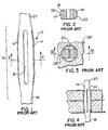
- Figures 1 and 2 show a prior art circuit board pin 10 having a compliant portion 12.
- the compliant portion is of the "eye of the needle" design in that it has two side-by-side beams 14 extending axially of the pin, the beams being spaced apart by an axially extending slot 16.
- the beams extend laterally beyond other portions 18 and 20 of the pin which extend from the two ends of the compliant portion 12.
- the pin is of constant thickness from end-to-end whereby the compliant portion, i.e. the beams 14, are no thicker than the other pin portions 18 and 20.
- Outer edges 22 of the two beams are convexly curved from end-to-end of the beams to provide an area of contact with lining material of a circuit board hole into which the pin is to be inserted.
- the prior art pin is assembled into a pin receiving hole 24 of a printed circuit board 26, as shown in Figures 3 and 4.
- the end 18 of the pin is inserted through the hole followed by the compliant portion 12.
- the distance across the edges 22 is slightly greater than the diameter of the hole whereby the hole resiliently flexes the beams inward towards each other, in known manner, thereby narrowing the slot 16 so that in the final position shown in Figures 3 and 4, the compliant section is resiliently held within the hole with the edges 22 resiliently pressing against the inside surface of the conductive lining material 28 of the hole.
- the contact surface area between the pin and the lining material 28 of the printed circuit board is small compared to the total inner surface of the lining material.
- the pressure applied by the small area of contact may result in cutting into the lining material to cause deterioration of the lining material and a reduction in the effectiveness of the circuit path.
- the width of the slot 16 is preferably made according to good machinery practice in a ratio of approximately 1:1 in relation to the thickness of the material of the pin.
- the slot 16 needs to be blanked from the material and the blanking of a slot with such a width to material ratio may be technically difficult.
- the present invention provides a circuit board pin and a method of producing such a pin which alleviates the above disadvantages. This is clear from the embodiment now to be described.
- a circuit board pin 30 according to the embodiment comprises a compliant portion 32 extending axially of the pin and other portions 34 and 36 of the pin extending axially from the two ends of the compliant portion.
- the compliant portion 32 is of the "eye of the needle” type of construction and has two side-by-side beams 38 which extend axially of the pin and are spaced apart by a longitudinally extending slot 40 over the compliant portion.
- the portions 34 and 36 of the pin are of rectangular or square cross-section and have edge surfaces 42 ( Figures 5 and 6) beyond which the beams 38 extend.
- the pin 30 is also similar to the pin 10 of the prior art.
- the pin 30 differs however from the prior art pin in the manner shown in Figures 6 and 7.
- the two beams 38 not only extend outwardly beyond the surfaces 42, but also extend outwardly beyond the other surfaces 44 of the rectangular pin portions 34 and 36.
- the beams 38 have oppositely outwardly facing surfaces 46 which are convex in lateral cross-section of the beams as shown in Figure 6. These surfaces extend outwardly beyond the surfaces 42 because the beams extend beyond these surfaces as has been described.
- the surfaces 46 have a lateral width (as shown in Figure 6) which is greater than the distance between the surfaces 44. Surfaces 46 extend beyond surfaces 44 to positions 48 which approximately lie at the remote positions of the beams.
- the surfaces 46 both in plan view ( Figure 5) and side elevational view ( Figure 7), extend outwardly beyond the boundaries of the pin portions 34 and 36, these boundaries being the surfaces 42 and 44.
- the compliant portion tapers down into the portions 34 and 36 to effect a merging together of the beams and also into the other portions beyond the ends of the slot 40. This tapering action occurs both in the plan view of Figure 5 and the side elevational view of Figure 7.
- the pin 30 provides a greater surface area (i.e. surfaces 46) for electrical contact with lining material in a pin receiving hole of a circuit board, than is possible with the surface area of the prior art pin.
- the pin 30 is fitted into a pin receiving hole 51 of a printed circuit board 50 ( Figure 8) in the manner of insertion described with regard to the pin 10.
- the pin 30 is held in position by reception of its compliant portion 32 within the layer 52 of conductive material forming the hole of the printed circuit board.
- the surfaces 46 having the correct characteristic of curvature to suit the inner diameter of the insulation, it will be appreciated that a substantial arc 54 of contact occurs between each surface 46 and the conductive layer 52 and that this arc of contact far exceeds anything possible between the prior art pin 10 and the conductive lining material of its associated hole.
- the arc 54 of contact between the two surfaces extends substantially beyond the surfaces 44 of the portions 34 and 36 of the pin.
- the larger arc of contact between the two surfaces proportionally increases the area of conductive contact between the beams and the lining material.
- the substantially wide convex surfaces 46 provide a further function.
- the contact area between surfaces 46 and the conductive layer 52 is substantially large compared to prior art arrangements, then there is a resultant decrease in pressure applied to the lining material by the resilient flexing of the beams 38 although the resilient outward load may be comparable to that in the prior art beams.
- the reduction in pressure reduces any tendency for the beams to cut into the insulation layer 52 whereby the tendency for deterioration of the printed circuit board and for reduction in the conductive path is minimized in the embodiment. It follows that in use of the circuit board pin according to the embodiment and as defined according to the invention, an improved circuit path is provided into a printed circuit board with reduced possibilities of damage resulting to the board or in a reduction in the electrical performance of the assembly.
- the pin 30 is made by the method and apparatus described with reference to Figure 9 onwards.
- the pin 30 is formed as one of a succession of pins from a rectangular cross-section wire 56 shown chain-dotted in Figure 9.
- the wire is drawn wire having substantially perfectly smooth side edges 58 across a width dimension of the wire, and top and bottom surfaces 44 across a thickness dimension of the wire, ( Figure 10), the surfaces 44 corresponding to the surfaces 44 of a finished pin.
- a pin preform 60 is formed at the leading end of the wire and is removed from the wire before formation of a subsequent pin preform.
- Each pin preform is provided, in a conventional manner for forming pin preforms from drawn wire, by reducing the width of the wire in two axially spaced regions 62 and 64 which are separated by an intermediate region 65 which is to become a preform for the compliant portion.
- the width of the wire is reduced by removal of the wire material from each surface 57 in a symmetrical fashion whereby the final cross-sectional shape and size of the pin portions 34 and 36 are produced upon the pin preform.
- the intermediate region 65 progressively tapers into the pin regions 34 and 36 as shown by Figure 9.
- a slot 16a is provided extending longitudinally of the intermediate region 65, and this defines two rectangularly shaped beams 38a having outer lateral edges 58.
- the ratio of the width of the slot 16a to the thickness of the wire, i.e. between surfaces 44, is substantially greater than 1:1 as this width of slot is easier to blank out.
- the wire is then fed forwardly to locate the pin preform 60 in a pin location station within apparatus which includes means for forming the completed compliant portion of the pin.
- the intermediate region 65 is located between two pressure applying elements 66 which are movable towards each other and apart horizontally, between guides 68, towards and away from the pin location station.
- the elements 66 have concave opposing surfaces 70 for forming the oppositely outwardly facing convex surfaces 46 on the beams.
- the apparatus includes two pressure resisting members 72 which are movable towards each other and apart in a vertical plane and partly across the pin location station.
- the two pressure resisting members 72 are also guided between the guides 68 and have reduced width ends 74 for location within the hole 16a as will be described.
- the reduced ends merge into greater width parts of the members 72 by inclined surfaces 76.
- the elements 66 and members 72 are movable between positions apart shown in Figure 11 and inner or positions closer together as shown in Figures 13 and 14.
- the concave surfaces 70 and the side and inclined surfaces of ends 74 of members 72 define two cavities 78 for shaping the beams 38 and for producing the taper into pin portions 34 and 36.
- the apparatus is provided with means for holding the length of material, i.e. the drawn wire, during deformation of the preform 60 to make the compliant portion.
- the holding means comprises vertically movable clamping members 80, which are moved to inner clamping positions (as shown in Figure 12) before movement of members 72 into their inner positions.
- These clamping members 80 have clamping surfaces 82 for engagement with the surfaces 44 of the pin portions 34 and 36.
- the pin blank 60 is located in its pin location station with the intermediate region 65 disposed between the outwardly positioned elements 66 and members 72.
- the clamping members 80 and the pressure resisting members 72 are then moved to their inner positions in which the clamping members clamp against the surfaces 44 of the pin regions 34 and 36 and the members 72 enter into the slot 16a until they abut each other as shown by Figure 13. In this position, the inclined surfaces 76 of the members 72 also lie partly within the slots 16a.
- the elements 66 are then moved inwardly from the position in Figure 13 to that of Figure 14.
- the surfaces 70 engage the outer lateral edges 58 of the beams 38a and progressively coin them so as to provide the convex surfaces 46 and also to displace the material in the beams 38a laterally into parts of the cavity 78.
- the material in the beams 38a becomes displaced beyond the surfaces 44, as shown in the finished structure of Figure 6.
- the surfaces 46 are formed with their lateral width greater than the original thickness of the wire itself.
- the material of the beams 38a is displaced inwardly against the reduced ends 74 of the members 72 so as to reduce the width of the slot 16a to a desired width to thickness of material ratio, e.g. around 1:1. This ratio has thus been produced while avoiding the usual difficult blanking operation to produce such a ratio of slot width to material thickness.
- the edges 58 were particularly smooth at the beginning of the coining operation so that coining is only required to reshape the surfaces to form the surfaces 46 and operations are not required substantially to enhance smoothness of the surface.
- the coining operation merely retains the smoothness of the surface during deformation.
- the coining operation provides some lateral grain flow in the material of the beams thereby increasing their strength beyond that provided by the grain flow extending axially of the pin and inherent from the drawn wire.
- the pin together with other pins may be assembled in spaced side-by-side relationship, i.e. in the form of a conventional "bandolier", for any further operations upon the pins to finish the end portions 34 and 36.
Landscapes
- Multi-Conductor Connections (AREA)
- Coupling Device And Connection With Printed Circuit (AREA)
- Printing Elements For Providing Electric Connections Between Printed Circuits (AREA)
Applications Claiming Priority (2)
| Application Number | Priority Date | Filing Date | Title |
|---|---|---|---|
| US77824 | 1979-09-21 | ||
| US07/077,824 US4769907A (en) | 1987-07-27 | 1987-07-27 | Method of making a circuit board pin |
Publications (2)
| Publication Number | Publication Date |
|---|---|
| EP0301730A2 true EP0301730A2 (de) | 1989-02-01 |
| EP0301730A3 EP0301730A3 (de) | 1990-03-21 |
Family
ID=22140263
Family Applications (1)
| Application Number | Title | Priority Date | Filing Date |
|---|---|---|---|
| EP88306422A Withdrawn EP0301730A3 (de) | 1987-07-27 | 1988-07-13 | Stift für gedruckte Schaltungen |
Country Status (3)
| Country | Link |
|---|---|
| US (1) | US4769907A (de) |
| EP (1) | EP0301730A3 (de) |
| JP (1) | JPS6486464A (de) |
Cited By (4)
| Publication number | Priority date | Publication date | Assignee | Title |
|---|---|---|---|---|
| EP0522613A1 (de) * | 1991-07-12 | 1993-01-13 | Connector Systems Technology N.V. | Elektrischer Kontaktstift für gedruckte Schaltungsplatten |
| WO1998042043A1 (en) * | 1997-03-14 | 1998-09-24 | Kam Circuits Limited | Improvements relating to printed circuit board pin location |
| WO2005122337A1 (de) * | 2004-06-09 | 2005-12-22 | Andreas Veigel | Einpresskontakt und verfahren zu dessen herstellung |
| US9685719B2 (en) | 2013-08-27 | 2017-06-20 | J.S.T. Mfg. Co., Ltd. | Press-fit terminal, connector incorporating same, press-fit continuous press-fit terminal body, and winding body of the continuous press-fit terminal body |
Families Citing this family (27)
| Publication number | Priority date | Publication date | Assignee | Title |
|---|---|---|---|---|
| US4828514A (en) * | 1988-01-21 | 1989-05-09 | Gte Products Corporation | Electrical connector with compliant section |
| US5078612A (en) * | 1988-10-06 | 1992-01-07 | Rozmus John J | Electrical contacts |
| US4909746A (en) * | 1989-05-31 | 1990-03-20 | Amp Incorporated | Contact for stackable electrical connector |
| GB2245770B (en) * | 1990-06-01 | 1994-09-21 | Oxley Dev Co Ltd | Compliant pins |
| US5061209A (en) * | 1991-03-13 | 1991-10-29 | Hubbell Incorporated | Wall plate jack and contact therefor |
| JP2576517Y2 (ja) * | 1991-12-10 | 1998-07-16 | ヒロセ電機 株式会社 | プレスフィットピン |
| US5487684A (en) * | 1992-07-01 | 1996-01-30 | Berg Technology, Inc. | Electrical contact pin for printed circuit board |
| US5337477A (en) * | 1993-07-21 | 1994-08-16 | Amcast Industrial Corporation | Methods and apparatus for forming tubular risers and manifolds including tubular risers |
| DE4400499C2 (de) * | 1994-01-11 | 1996-05-02 | Itt Cannon Gmbh | Kontaktfeder-Anordnung |
| US5823830A (en) * | 1995-02-24 | 1998-10-20 | Wurster; Woody | Tailess compliant contact |
| DE19508133C2 (de) * | 1995-03-08 | 1997-02-13 | Kostal Leopold Gmbh & Co Kg | Stiftförmiges Kontaktelement |
| EP0777306B1 (de) * | 1995-12-01 | 2000-07-26 | Berg Electronics Manufacturing B.V. | Glatte Kontaktelemente, Verfahren zur Herstellung solcher Elemente und Produkte mit solchen Elementen |
| US6260268B1 (en) | 1999-08-11 | 2001-07-17 | Positronic Industries, Inc. | Method of forming a solid compliant pin connector contact |
| GB0016787D0 (en) | 2000-07-07 | 2000-08-30 | Pfizer Ltd | Compounds useful in therapy |
| DE10229331B4 (de) * | 2002-06-29 | 2016-03-24 | Conti Temic Microelectronic Gmbh | Einpresskontakt |
| CN101568227B (zh) * | 2004-03-31 | 2011-09-28 | 三菱电线工业株式会社 | 电路基板及其制造方法和采用该电路基板的接线箱 |
| US7377823B2 (en) * | 2005-05-23 | 2008-05-27 | J.S.T. Corporation | Press-fit pin |
| DE102006011657A1 (de) * | 2006-03-12 | 2007-09-20 | Kramski Gmbh | Kontaktstift und Verfahren zu dessen Herstellung |
| US8087281B2 (en) * | 2008-08-06 | 2012-01-03 | Bead Industries, Inc. | Method to continuously form surface mount flanged pins |
| JP2013131364A (ja) * | 2011-12-21 | 2013-07-04 | Sumitomo Wiring Syst Ltd | 端子金具及び端子金具の接続構造 |
| JP5831509B2 (ja) * | 2013-08-09 | 2015-12-09 | 第一精工株式会社 | プレスフィット用コネクタ端子およびその製造方法 |
| US9276338B1 (en) | 2014-06-24 | 2016-03-01 | Emc Corporation | Compliant pin, electrical assembly including the compliant pin and method of manufacturing the compliant pin |
| JP6550890B2 (ja) * | 2015-04-22 | 2019-07-31 | 住友電装株式会社 | プレスフィット端子 |
| JP6953919B2 (ja) * | 2017-09-04 | 2021-10-27 | 株式会社デンソー | プレスフィット端子及び電子装置 |
| JP6735263B2 (ja) * | 2017-11-01 | 2020-08-05 | 矢崎総業株式会社 | プレスフィット端子及び回路基板のプレスフィット端子接続構造 |
| US11431141B1 (en) | 2019-08-06 | 2022-08-30 | Interplex Industries, Inc. | Method of manufacturing a press-fit contact |
| CN220692362U (zh) * | 2023-08-18 | 2024-03-29 | 陈俊瑞 | 鱼眼端子结构 |
Family Cites Families (9)
| Publication number | Priority date | Publication date | Assignee | Title |
|---|---|---|---|---|
| US533182A (en) * | 1895-01-29 | Island | ||
| US3545080A (en) * | 1967-05-16 | 1970-12-08 | Amp Inc | Method of making resilient pins |
| JPS5163460A (en) * | 1974-10-10 | 1976-06-01 | Du Pont | Kairobanpin oyobi hoho |
| DE2930560C2 (de) * | 1979-07-27 | 1982-03-04 | Siemens AG, 1000 Berlin und 8000 München | Verfahren zur Herstellung eines Klemmbereiches bei einem in einer Bohrung kraftschlüssig fixierbaren stiftförmigen Element |
| US4533204A (en) * | 1982-08-23 | 1985-08-06 | Minnesota Mining And Manufacturing Company | Resilient circuit board contact |
| US4576314A (en) * | 1983-11-16 | 1986-03-18 | Elias Abe G | Device for squeezing and winding collapsible tubes |
| US4621421A (en) * | 1984-09-17 | 1986-11-11 | Thomas & Betts Corporation | Method of making an electrical terminal |
| DE3513768A1 (de) * | 1985-04-17 | 1986-10-23 | Standard Elektrik Lorenz Ag, 7000 Stuttgart | Verfahren zur herstellung eines elektrischen kontaktstiftes fuer gedruckte schaltungsplatten und werkzeug zur durchfuehrung des verfahrens |
| DE3533339A1 (de) * | 1985-09-16 | 1987-03-26 | Siemens Ag | Verfahren zur herstellung von einpresszonen fuer kontaktteile |
-
1987
- 1987-07-27 US US07/077,824 patent/US4769907A/en not_active Expired - Lifetime
-
1988
- 1988-07-13 EP EP88306422A patent/EP0301730A3/de not_active Withdrawn
- 1988-07-26 JP JP63184775A patent/JPS6486464A/ja active Pending
Cited By (6)
| Publication number | Priority date | Publication date | Assignee | Title |
|---|---|---|---|---|
| EP0522613A1 (de) * | 1991-07-12 | 1993-01-13 | Connector Systems Technology N.V. | Elektrischer Kontaktstift für gedruckte Schaltungsplatten |
| WO1998042043A1 (en) * | 1997-03-14 | 1998-09-24 | Kam Circuits Limited | Improvements relating to printed circuit board pin location |
| WO2005122337A1 (de) * | 2004-06-09 | 2005-12-22 | Andreas Veigel | Einpresskontakt und verfahren zu dessen herstellung |
| KR100907966B1 (ko) * | 2004-06-09 | 2009-07-16 | 안드레아스 바이겔 | 압입 연결기구 및 그 제조방법 |
| US7891992B2 (en) | 2004-06-09 | 2011-02-22 | Andreas Veigel | Press-fit contact |
| US9685719B2 (en) | 2013-08-27 | 2017-06-20 | J.S.T. Mfg. Co., Ltd. | Press-fit terminal, connector incorporating same, press-fit continuous press-fit terminal body, and winding body of the continuous press-fit terminal body |
Also Published As
| Publication number | Publication date |
|---|---|
| EP0301730A3 (de) | 1990-03-21 |
| JPS6486464A (en) | 1989-03-31 |
| US4769907A (en) | 1988-09-13 |
Similar Documents
| Publication | Publication Date | Title |
|---|---|---|
| US4769907A (en) | Method of making a circuit board pin | |
| US4691979A (en) | Compliant press-fit electrical contact | |
| US5735717A (en) | Female terminal metal fixture | |
| CA1205989A (en) | Process for producing dual beam electrical contact | |
| JP3415140B1 (ja) | コネクタ | |
| JPH09217865A (ja) | 二つの部分から成るケーブル連結具 | |
| EP0984517A2 (de) | Elektrischer Büchsenkontakt | |
| CA1198490A (en) | Press fit pin | |
| US6431903B1 (en) | Insulation displacement contact for use with fine wires | |
| US5575696A (en) | Terminal receptacle | |
| US4740166A (en) | Circuit board pin | |
| US4831728A (en) | Method of making circuit board pin | |
| US3559604A (en) | Method of forming swaged contacts using progressive die | |
| CZ280589B6 (cs) | Způsob výroby svorky elektrického kontaktu vystřižením a ohýbáním | |
| CN100375342C (zh) | 连接器及其树脂模制方法 | |
| US5573431A (en) | Solderless contact in board | |
| US4932903A (en) | Elastically deformable electric contact elements for incorporation in connectors and methods of manufacturing said contact elements | |
| CA1293303C (en) | Circuit board pin | |
| US4825541A (en) | Method of making contact springs | |
| US5643017A (en) | Female terminal and method of producing the same | |
| CN100384031C (zh) | 端子及其制造方法 | |
| EP1278270B1 (de) | Verbindungsendstück | |
| EP0492017B1 (de) | Elektrischer Endverbinder mit zerbrechbarem Montagestift und Herstellverfahren dafür | |
| JPH0646586B2 (ja) | 雄端子の製造方法 | |
| US6155865A (en) | Insulation displacement contact terminal |
Legal Events
| Date | Code | Title | Description |
|---|---|---|---|
| PUAI | Public reference made under article 153(3) epc to a published international application that has entered the european phase |
Free format text: ORIGINAL CODE: 0009012 |
|
| AK | Designated contracting states |
Kind code of ref document: A2 Designated state(s): BE DE FR GB IT NL SE |
|
| PUAL | Search report despatched |
Free format text: ORIGINAL CODE: 0009013 |
|
| AK | Designated contracting states |
Kind code of ref document: A3 Designated state(s): BE DE FR GB IT NL SE |
|
| 17P | Request for examination filed |
Effective date: 19900606 |
|
| 17Q | First examination report despatched |
Effective date: 19911009 |
|
| STAA | Information on the status of an ep patent application or granted ep patent |
Free format text: STATUS: THE APPLICATION IS DEEMED TO BE WITHDRAWN |
|
| 18D | Application deemed to be withdrawn |
Effective date: 19920220 |