EP0301807A2 - Méthode pour contrôler un thyristor optique PNPN - Google Patents
Méthode pour contrôler un thyristor optique PNPN Download PDFInfo
- Publication number
- EP0301807A2 EP0301807A2 EP88306873A EP88306873A EP0301807A2 EP 0301807 A2 EP0301807 A2 EP 0301807A2 EP 88306873 A EP88306873 A EP 88306873A EP 88306873 A EP88306873 A EP 88306873A EP 0301807 A2 EP0301807 A2 EP 0301807A2
- Authority
- EP
- European Patent Office
- Prior art keywords
- pnpn thyristor
- thyristor
- optical
- anode
- cathode
- Prior art date
- Legal status (The legal status is an assumption and is not a legal conclusion. Google has not performed a legal analysis and makes no representation as to the accuracy of the status listed.)
- Granted
Links
Images


Classifications
-
- H—ELECTRICITY
- H10—SEMICONDUCTOR DEVICES; ELECTRIC SOLID-STATE DEVICES NOT OTHERWISE PROVIDED FOR
- H10H—INORGANIC LIGHT-EMITTING SEMICONDUCTOR DEVICES HAVING POTENTIAL BARRIERS
- H10H20/00—Individual inorganic light-emitting semiconductor devices having potential barriers, e.g. light-emitting diodes [LED]
- H10H20/80—Constructional details
- H10H20/81—Bodies
- H10H20/813—Bodies having a plurality of light-emitting regions, e.g. multi-junction LEDs or light-emitting devices having photoluminescent regions within the bodies
-
- G—PHYSICS
- G11—INFORMATION STORAGE
- G11C—STATIC STORES
- G11C11/00—Digital stores characterised by the use of particular electric or magnetic storage elements; Storage elements therefor
- G11C11/21—Digital stores characterised by the use of particular electric or magnetic storage elements; Storage elements therefor using electric elements
- G11C11/34—Digital stores characterised by the use of particular electric or magnetic storage elements; Storage elements therefor using electric elements using semiconductor devices
- G11C11/39—Digital stores characterised by the use of particular electric or magnetic storage elements; Storage elements therefor using electric elements using semiconductor devices using thyristors or the avalanche or negative resistance type, e.g. PNPN, SCR, SCS, UJT
-
- G—PHYSICS
- G11—INFORMATION STORAGE
- G11C—STATIC STORES
- G11C7/00—Arrangements for writing information into, or reading information out from, a digital store
- G11C7/005—Arrangements for writing information into, or reading information out from, a digital store with combined beam-and individual cell access
-
- H—ELECTRICITY
- H10—SEMICONDUCTOR DEVICES; ELECTRIC SOLID-STATE DEVICES NOT OTHERWISE PROVIDED FOR
- H10F—INORGANIC SEMICONDUCTOR DEVICES SENSITIVE TO INFRARED RADIATION, LIGHT, ELECTROMAGNETIC RADIATION OF SHORTER WAVELENGTH OR CORPUSCULAR RADIATION
- H10F55/00—Radiation-sensitive semiconductor devices covered by groups H10F10/00, H10F19/00 or H10F30/00 being structurally associated with electric light sources and electrically or optically coupled thereto
- H10F55/18—Radiation-sensitive semiconductor devices covered by groups H10F10/00, H10F19/00 or H10F30/00 being structurally associated with electric light sources and electrically or optically coupled thereto wherein the radiation-sensitive semiconductor devices and the electric light source share a common body having dual-functionality of light emission and light detection
Definitions
- the invention relates to a method for controlling an optical pnpn thyristor and more particularly to a method in which the optical pnpn thyristor is turned on to be held with reduced power consumption.
- An optical semiconductor memory in which light emission is performed with a small amount of trigger light to be continued even after the extinction of the trigger light is a basic device indispensable with an optical apparatus such as an optical switching, an information parallel processing system etc.
- optical semiconductor memory is described as an optical pnpn thyristor on pages 596 to 600 of "Journal of Applied Physics, 59(2), 15 January 1986".
- the conventional optical pnpn thyristor comprises an anode layer of p-AlGaAs, a cathode layer of n-AlGaAs, and a gate layer sandwiched between the anode and cathode layers wherein the gate layer is of a forbidden band narrower than those of the anode and cathode layers and includes an n-gate layer of n-GaAs and a p-gate layer of p-GaAs.
- the pnpn thyristor is turned on to be shifted from a high impedance state to a low impedance state wherein carriers are mainly injected into the n-gate layer to be confined therein thereby emitting light with a high light emission efficiency. If a predetermined bias voltage less than a turning-on voltage is applied across the anode and cathode layers, light emission is continued even after the extinction of a trigger light so that the pnpn thyristor can be used for an optical memory.
- the value of 150mW is much higher so that it is difficult to put the pnpn thyristor into a practical use due to a construction that pnpn thyristors of the number as much as required must be arranged on a wafer.
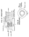
- 1A and 1B show the pnpn thyristor which comprises a contact layer 31 of P+-GaAs, a buffer layer 32 of P+-GaAs having a thickness of 0.3 ⁇ m, an anode layer 33 of P+-AlGaAs having a thickness of 0.5 ⁇ m, an n-gate layer 34 of n-GaAs having a thickness of 1 ⁇ m, a P+-gate layer 35 of P+-GaAs having a thickness of 30 ⁇ , a cathode layer 36 of n-AlGaAs having a thickness of 400 ⁇ , a contact layer 37 of n+-GaAs having a thickness of 0.5 ⁇ m, an anode electrode 30 formed on the back surface of the contact layer 31, and a cathode electrode 38 having an aperture 38A for trigger and output lights formed on the top surface of the contact layer 37.
- the n and P+- gater layers 34 and 35 are sandwich
- a state thereof is shifted from a high impedance to a low impedance, and carriers are mainly injected into the n-gate layer 34 and confined therein to result in light emission therefrom.
- a high light emission efficiency is obtained because the gate layer including the n and P+-gate layers 34 and 35 is sandwiched between the anode and cathode layers 33 and 36 having wider forbidden bands than that of the gate layer.
- Figs. 2 and 3 show a conventional process for controlling such an optical pnpn thyristor to be driven wherein voltage V b less than a switching voltage V s by which a high impedance state is shifted to a low impedance state is applied to an optical pnpn thyristor.
- the pnpn thyristor is turned on to emit light when trigger light is supplied thereto.
- the voltage V b is not less than voltage V h as shown in Fig. 2 even if the voltage V b is decreased down to the voltage V h after the turning-on of the pnpn thyristor, the low impedance state is maintained therein.
- the voltage V h is defined as a holding voltage.
- V b 1.5V which is more than the holding voltage V h is applied across anode and cathode layers thereof as described before. Therefore, there is the aforementioned disadvantage in the conventional process for controlling an optical pnpn thyristor to be driven.
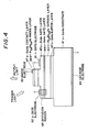
- Fig. 4 shows an optical pnpn thyristor used in an experiment in which a process for controlling an optical pnpn thyristor to be driven according to the invention is embodied as described later.
- the optical pnpn thyristor comprises a buffer layer 42 of n-GaAs having a thickness of 0.5 ⁇ m and a carrier density of 2x1018cm ⁇ 3 on a substrate 41 of n-GaAs, a cathode layer 43 of n-Al 0.4 Ga 0.6 As having a thickness of 1 ⁇ m and a carrier density of 5x1017cm ⁇ 3, a p-gate layer 44 of p-GaAs having a thickness of 50 ⁇ and a carrier density of 1x1019cm ⁇ 3, an n-gate layer 45 of n-GaAs having a thickness of 1 ⁇ m and a carrier density of 1x1017cm ⁇ 3, an anode layer 46 of p-Al 0.4 Ga 0.6
- the optical pnpn thyristor further comprises a cathode electrode 49 provided on the back surface of the substrate 41, an anode electrode 50 provided on the top surface of the contact layer 47, an n-gate electrode 51 provided on the n-gate layer 45, and a p-gate electrode 52 provided on a diffusion region 48 diffused through the n-gate layer 45 and the p-gate layer 44 into the cathode layer 43 with Z n .
- a cathode region is composed of the cathode layer 43, the buffer layer 42 and the substrate 41
- an anode region is composed of the contact layer 47 and the anode layer 46.
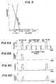
- the size of the pnpn thyristor described above is 100 ⁇ m x 100 ⁇ m, and a switching voltage V s and a holding voltage V h are 6.2V and 1.5V, respectively as shown in Fig. 5.
- the holding voltage V h is detected visually on a display of a curve tracer in accordance with a measured curve of current and voltage.
- the invention is based on a finding that ON state is stored in an optical pnpn thyristor for a minute time even if a bias voltage V b is decreased less than a holding voltage V h under ON state of the pnpn thyristor.
- the pnpn thyristor as shown in Fig. 4 light output is improved to be 200 ⁇ W with current of 100mA in a low impedance state thereof as compared to the conventional pnpn thyristor because a layer structure thereof is improved.
- the pulse interval is less than a period during which ON state is stored in the pnpn thyristor even if a bias voltage V b is decreased less than a holding voltage V h .
- no current flowing response is observed in a range of illustration in Fig. 6C because the pnpn thyristor operates in a region where a differential resistance for a current and voltage characteristic is very large.
- an amount of carriers injected by one of the intermittent pulses 313, that is, current value induced therein is inevitably small.
- an electric power consumption of 13 ⁇ W which is a holding electric power is resulted from the application of the intermittent pulse 313.
- the pulse width is 500 ns, it may be shorter than that period during which ON state is held.
- a holding current is measured to be several ⁇ A in accordance with a current and voltage characteristic of a curve tracer when a holding voltage V h is 1.5V.
- a holding electric power can be decreased down to several ⁇ W (several ⁇ A x 1.5V) per one element of the pnpn thyristor.
- ⁇ W severe ⁇ A x 1.5V
- the electric power will be proportionally low.
- a set pulse 312 is applied to the anode and cathode electrodes 46 and 43 thereof without supplying trigger light to the pnpn thyristor (FIGS, 6A and 6B) so that light emission and current flowing response are obtained (FIGS. 6C and 6D).
- a current flowing response time is less than 1 ns, while a time during which light output is increased from zero to a normal value is approximately 20 ns. This is a reason why a response time of light output depends on a light emission recombination life of injected carriers.
- an optical pnpn thyristor is turned on to provide light emission by a positive bias voltage applied across an anode and cathode electrodes thereof and trigger light supplied thereto, the light emission is ceased and an information of a fact that light is supplied thereto is erased when the bias voltage is turned off. For this reason, the positive bias voltage is kept to be applied across the anode and cathode electrodes thereof so that the information is stored therein.
- the inventors found in their experiment that ON state is held in a pnpn thyristor for a minute time even if a bias voltage is turned off. In such a pnpn thyristor, it is necessary to expel excess carriers from three forward biased pn junctions thereby restoring a high impedance state from a low impedance state as shown in Figs. 7A to 7°C. Even if a bias voltage is dropped down to zero before completing the restoration of a high impedance state, the low impedance state is held. In the experiment, it is confirmed that a time during which the low impedance state is held under no bias voltage is several hundreds ns to several tens ⁇ s.
- ON state holding time on the horizontal axis is linearly proportional to a bias voltage on the vertical axis which is less than a holding voltage V h .
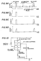
- a bias voltage V b1 less than a peak value of intermittent pulses 313 is constantly applied, as shown in Fig. 9A, across an anode and cathode electrodes of an optical pnpn thyristor which is turned on to be in a low impedance state by a set pulse 311, which is kept to remain in the low impedance state by the intermittent pulses 313, and which is again turned on to emit light for the reading of information stored therein by a set pulse 312.
- a high speed turning off (erasing) process of an optical pnpn thyristor will be explained in Fig. 10.
- a negative reset pulse is applied across the anode and cathode electrodes of the pnpn thyristor.
- the n and p-gate electrodes are provided wherein a resistance 60 of 10k ⁇ is connected between the n-gate electrode 51 and the ground, and a Shottky diode 61 (for instance, 15512M of NEC Corporation) is connected between the anode electrode 50 and the p-gate electrode 52, provided that a resistance 62 connected between the cathode electrode 49 and the ground is a series resistance for adjusting a value of current which flows during ON state of the pnpn thyristor.
- a switching voltage V s is decreased from 6.2V to 2.4V for the reason why electrons are injected through the resistance 60 into the n-gate layer.
- a high speed erasing of ON state can be realized in the presence of a bypass for pulling out excess carriers at a time of resetting the pnpn thyristor.
- the invention relates to a process for controlling an optical pnpn thyristor which is applicable to an image processing, an optical logic calculation etc. wherein ON state of the pnpn thyristor is held by applying intermittent pulses with a predetermined pulse interval after an optical information is written into the pnpn thyristor.
- a set pulse is applied to the pnpn thyristor only when light emission is required to read the optical information therefrom.
- electric power is prevented from being consumed more than necessary in a time storing the optical information so that an optical memory with less electric power consumption can be realized for the first time.
Landscapes
- Engineering & Computer Science (AREA)
- Computer Hardware Design (AREA)
- Thyristors (AREA)
- Electronic Switches (AREA)
- Light Receiving Elements (AREA)
Applications Claiming Priority (2)
| Application Number | Priority Date | Filing Date | Title |
|---|---|---|---|
| JP62188189A JPS6431134A (en) | 1987-07-27 | 1987-07-27 | Driving method for pnpn optical thyristor |
| JP188189/87 | 1987-07-27 |
Publications (3)
| Publication Number | Publication Date |
|---|---|
| EP0301807A2 true EP0301807A2 (fr) | 1989-02-01 |
| EP0301807A3 EP0301807A3 (en) | 1990-07-18 |
| EP0301807B1 EP0301807B1 (fr) | 1993-10-06 |
Family
ID=16219324
Family Applications (1)
| Application Number | Title | Priority Date | Filing Date |
|---|---|---|---|
| EP88306873A Expired - Lifetime EP0301807B1 (fr) | 1987-07-27 | 1988-07-26 | Méthode pour contrôler un thyristor optique PNPN |
Country Status (4)
| Country | Link |
|---|---|
| US (1) | US4864168A (fr) |
| EP (1) | EP0301807B1 (fr) |
| JP (1) | JPS6431134A (fr) |
| DE (1) | DE3884709T2 (fr) |
Cited By (2)
| Publication number | Priority date | Publication date | Assignee | Title |
|---|---|---|---|---|
| GB2253303A (en) * | 1991-02-12 | 1992-09-02 | Mitsubishi Electric Corp | A semiconducter light emitting device |
| EP0454168A3 (en) * | 1990-04-27 | 1993-04-21 | Nec Corporation | Driving method and apparatus of a pnpn semiconductor device |
Families Citing this family (21)
| Publication number | Priority date | Publication date | Assignee | Title |
|---|---|---|---|---|
| JPH03108815A (ja) * | 1989-09-21 | 1991-05-09 | Nec Corp | ゲート付pnpn半導体素子の駆動回路及び駆動方法 |
| US5204871A (en) * | 1990-03-29 | 1993-04-20 | Larkins Eric C | Bistable optical laser based on a heterostructure pnpn thyristor |
| US5625636A (en) * | 1991-10-11 | 1997-04-29 | Bryan; Robert P. | Integration of photoactive and electroactive components with vertical cavity surface emitting lasers |
| US5319182A (en) * | 1992-03-04 | 1994-06-07 | Welch Allyn, Inc. | Integrated solid state light emitting and detecting array and apparatus employing said array |
| JP3016302B2 (ja) * | 1992-04-23 | 2000-03-06 | 日本電気株式会社 | pnpn半導体素子とその駆動回路 |
| US5291041A (en) * | 1993-03-01 | 1994-03-01 | The United States Of America As Represented By The Secretary Of The Army | AlGaAs/GaAs thyristor |
| US5469088A (en) * | 1993-03-19 | 1995-11-21 | Advanced Micro Devices, Inc. | Cascade array cell partitioning for a sense amplifier of a programmable logic device |
| US5798520A (en) * | 1996-07-31 | 1998-08-25 | Imec Vzw | Cell for optical-to-electrical signal conversion and amplification, and operation method thereof |
| US6154477A (en) * | 1997-05-13 | 2000-11-28 | Berkeley Research Associates, Inc. | On-board laser-triggered multi-layer semiconductor power switch |
| US6229161B1 (en) * | 1998-06-05 | 2001-05-08 | Stanford University | Semiconductor capacitively-coupled NDR device and its applications in high-density high-speed memories and in power switches |
| US6690038B1 (en) | 1999-06-05 | 2004-02-10 | T-Ram, Inc. | Thyristor-based device over substrate surface |
| US6462359B1 (en) | 2001-03-22 | 2002-10-08 | T-Ram, Inc. | Stability in thyristor-based memory device |
| US7456439B1 (en) | 2001-03-22 | 2008-11-25 | T-Ram Semiconductor, Inc. | Vertical thyristor-based memory with trench isolation and its method of fabrication |
| US6727528B1 (en) | 2001-03-22 | 2004-04-27 | T-Ram, Inc. | Thyristor-based device including trench dielectric isolation for thyristor-body regions |
| US6891205B1 (en) | 2001-03-22 | 2005-05-10 | T-Ram, Inc. | Stability in thyristor-based memory device |
| WO2002082504A2 (fr) * | 2001-04-05 | 2002-10-17 | T-Ram, Inc. | Restauration des donnees dans une memoire a thyristors |
| US6666481B1 (en) | 2002-10-01 | 2003-12-23 | T-Ram, Inc. | Shunt connection to emitter |
| US6965129B1 (en) | 2002-11-06 | 2005-11-15 | T-Ram, Inc. | Thyristor-based device having dual control ports |
| US6944051B1 (en) | 2003-10-29 | 2005-09-13 | T-Ram, Inc. | Data restore in thryistor based memory devices |
| US7989841B1 (en) | 2007-07-31 | 2011-08-02 | Hewlett-Packard Development Company, L.P. | Fast injection optical switch |
| DE102013113010A1 (de) * | 2013-11-25 | 2015-05-28 | Osram Opto Semiconductors Gmbh | Strahlungsemittierendes Halbleiterbauelement |
Family Cites Families (5)
| Publication number | Priority date | Publication date | Assignee | Title |
|---|---|---|---|---|
| FR2175571B1 (fr) * | 1972-03-14 | 1978-08-25 | Radiotechnique Compelec | |
| FR2175574B1 (fr) * | 1972-03-14 | 1975-08-29 | Radiotechnique Compelec | |
| FR2273371B1 (fr) * | 1974-05-28 | 1978-03-31 | Thomson Csf | |
| DE3405769A1 (de) * | 1984-02-17 | 1985-08-22 | Siemens AG, 1000 Berlin und 8000 München | Verfahren und vorrichtung zum ansteuern des stromleitenden zustandes eines abschaltbaren thyristors |
| US4806997A (en) * | 1985-06-14 | 1989-02-21 | AT&T Laboratories American Telephone and Telegraph Company | Double heterostructure optoelectronic switch |
-
1987
- 1987-07-27 JP JP62188189A patent/JPS6431134A/ja active Granted
-
1988
- 1988-07-25 US US07/223,600 patent/US4864168A/en not_active Expired - Lifetime
- 1988-07-26 EP EP88306873A patent/EP0301807B1/fr not_active Expired - Lifetime
- 1988-07-26 DE DE88306873T patent/DE3884709T2/de not_active Expired - Fee Related
Cited By (4)
| Publication number | Priority date | Publication date | Assignee | Title |
|---|---|---|---|---|
| EP0454168A3 (en) * | 1990-04-27 | 1993-04-21 | Nec Corporation | Driving method and apparatus of a pnpn semiconductor device |
| GB2253303A (en) * | 1991-02-12 | 1992-09-02 | Mitsubishi Electric Corp | A semiconducter light emitting device |
| US5272362A (en) * | 1991-02-12 | 1993-12-21 | Mitsubishi Denki Kabushiki Kaisha | Semiconductor light emitting device |
| GB2253303B (en) * | 1991-02-12 | 1995-07-12 | Mitsubishi Electric Corp | A semiconductor light emitting device |
Also Published As
| Publication number | Publication date |
|---|---|
| EP0301807B1 (fr) | 1993-10-06 |
| EP0301807A3 (en) | 1990-07-18 |
| JPH0561810B2 (fr) | 1993-09-07 |
| JPS6431134A (en) | 1989-02-01 |
| US4864168A (en) | 1989-09-05 |
| DE3884709D1 (de) | 1993-11-11 |
| DE3884709T2 (de) | 1994-05-05 |
Similar Documents
| Publication | Publication Date | Title |
|---|---|---|
| EP0301807B1 (fr) | Méthode pour contrôler un thyristor optique PNPN | |
| Kasahara et al. | Double heterostructure optoelectronic switch as a dynamic memory with low‐power consumption | |
| CN110556707B (zh) | 发光装置、光测量装置及图像形成装置 | |
| US4103312A (en) | Semiconductor memory devices | |
| US5869845A (en) | Resonant tunneling memory | |
| US5936258A (en) | Optical semiconductor memory device and read/write method therefor | |
| EP0273344B1 (fr) | PNPN-Thyristor | |
| CA1085053A (fr) | Memoire a transistors a effet de champ en mode de depletion | |
| US7244997B2 (en) | Magneto-luminescent transducer | |
| EP0288267B1 (fr) | Dispositif optique à semi-conducteur | |
| US4975750A (en) | Semiconductor device | |
| JPH08153890A (ja) | 発光サイリスタおよび自己走査型発光装置 | |
| US5028969A (en) | Semiconductor device for a space modulation matrix and method for driving a space modulation matrix | |
| US6509886B2 (en) | Two-dimensional light-emitting element array device and method for driving the same | |
| US3855583A (en) | Conductor-insulator-junction (cij) optical memory device and a memory system dependent thereon | |
| US5340998A (en) | Semiconductor surface light emitting and receiving heterojunction device | |
| EP0632510A2 (fr) | Dispositif semi-conducteur émetteur de lumière et sa méthode de fabrication | |
| JP2503597B2 (ja) | pnpn半導体素子の駆動方法及びスイッチング素子の駆動方法 | |
| EP0366424B1 (fr) | Méthode d'attaque d'un dispositif PNPN à semi-conducteur | |
| US4212082A (en) | Method for fabrication of improved storage target and target produced thereby | |
| US5321294A (en) | Shift register having optically bistable elements coupled by an optical waveguide layer | |
| US5084748A (en) | Semiconductor optical memory having a low switching voltage | |
| JP2861069B2 (ja) | pnpn半導体素子の駆動方法 | |
| US4733399A (en) | Semiconductor laser device having integral optical output modulator | |
| CA2001332C (fr) | Methode d'attaque pour dispositif a semiconducteur pnpn |
Legal Events
| Date | Code | Title | Description |
|---|---|---|---|
| PUAI | Public reference made under article 153(3) epc to a published international application that has entered the european phase |
Free format text: ORIGINAL CODE: 0009012 |
|
| 17P | Request for examination filed |
Effective date: 19880805 |
|
| AK | Designated contracting states |
Kind code of ref document: A2 Designated state(s): DE FR GB |
|
| PUAL | Search report despatched |
Free format text: ORIGINAL CODE: 0009013 |
|
| AK | Designated contracting states |
Kind code of ref document: A3 Designated state(s): DE FR GB |
|
| 17Q | First examination report despatched |
Effective date: 19920710 |
|
| GRAA | (expected) grant |
Free format text: ORIGINAL CODE: 0009210 |
|
| AK | Designated contracting states |
Kind code of ref document: B1 Designated state(s): DE FR GB |
|
| PG25 | Lapsed in a contracting state [announced via postgrant information from national office to epo] |
Ref country code: FR Effective date: 19931006 |
|
| REF | Corresponds to: |
Ref document number: 3884709 Country of ref document: DE Date of ref document: 19931111 |
|
| EN | Fr: translation not filed | ||
| PLBE | No opposition filed within time limit |
Free format text: ORIGINAL CODE: 0009261 |
|
| STAA | Information on the status of an ep patent application or granted ep patent |
Free format text: STATUS: NO OPPOSITION FILED WITHIN TIME LIMIT |
|
| 26N | No opposition filed | ||
| REG | Reference to a national code |
Ref country code: GB Ref legal event code: IF02 |
|
| PGFP | Annual fee paid to national office [announced via postgrant information from national office to epo] |
Ref country code: GB Payment date: 20050720 Year of fee payment: 18 |
|
| PGFP | Annual fee paid to national office [announced via postgrant information from national office to epo] |
Ref country code: DE Payment date: 20050721 Year of fee payment: 18 |
|
| PG25 | Lapsed in a contracting state [announced via postgrant information from national office to epo] |
Ref country code: GB Free format text: LAPSE BECAUSE OF NON-PAYMENT OF DUE FEES Effective date: 20060726 |
|
| PG25 | Lapsed in a contracting state [announced via postgrant information from national office to epo] |
Ref country code: DE Free format text: LAPSE BECAUSE OF NON-PAYMENT OF DUE FEES Effective date: 20070201 |
|
| GBPC | Gb: european patent ceased through non-payment of renewal fee |
Effective date: 20060726 |