EP0301862A2 - Transistors à haute mobilité électronique - Google Patents
Transistors à haute mobilité électronique Download PDFInfo
- Publication number
- EP0301862A2 EP0301862A2 EP88306966A EP88306966A EP0301862A2 EP 0301862 A2 EP0301862 A2 EP 0301862A2 EP 88306966 A EP88306966 A EP 88306966A EP 88306966 A EP88306966 A EP 88306966A EP 0301862 A2 EP0301862 A2 EP 0301862A2
- Authority
- EP
- European Patent Office
- Prior art keywords
- semiconductive layer
- layer
- semiconductive
- alinas
- gate
- Prior art date
- Legal status (The legal status is an assumption and is not a legal conclusion. Google has not performed a legal analysis and makes no representation as to the accuracy of the status listed.)
- Withdrawn
Links
Images

Classifications
-
- H—ELECTRICITY
- H10—SEMICONDUCTOR DEVICES; ELECTRIC SOLID-STATE DEVICES NOT OTHERWISE PROVIDED FOR
- H10D—INORGANIC ELECTRIC SEMICONDUCTOR DEVICES
- H10D30/00—Field-effect transistors [FET]
- H10D30/40—FETs having zero-dimensional [0D], one-dimensional [1D] or two-dimensional [2D] charge carrier gas channels
- H10D30/47—FETs having zero-dimensional [0D], one-dimensional [1D] or two-dimensional [2D] charge carrier gas channels having two-dimensional [2D] charge carrier gas channels, e.g. nanoribbon FETs or high electron mobility transistors [HEMT]
- H10D30/471—High electron mobility transistors [HEMT] or high hole mobility transistors [HHMT]
- H10D30/473—High electron mobility transistors [HEMT] or high hole mobility transistors [HHMT] having confinement of carriers by multiple heterojunctions, e.g. quantum well HEMT
-
- H—ELECTRICITY
- H10—SEMICONDUCTOR DEVICES; ELECTRIC SOLID-STATE DEVICES NOT OTHERWISE PROVIDED FOR
- H10D—INORGANIC ELECTRIC SEMICONDUCTOR DEVICES
- H10D30/00—Field-effect transistors [FET]
- H10D30/40—FETs having zero-dimensional [0D], one-dimensional [1D] or two-dimensional [2D] charge carrier gas channels
- H10D30/47—FETs having zero-dimensional [0D], one-dimensional [1D] or two-dimensional [2D] charge carrier gas channels having two-dimensional [2D] charge carrier gas channels, e.g. nanoribbon FETs or high electron mobility transistors [HEMT]
-
- H—ELECTRICITY
- H10—SEMICONDUCTOR DEVICES; ELECTRIC SOLID-STATE DEVICES NOT OTHERWISE PROVIDED FOR
- H10D—INORGANIC ELECTRIC SEMICONDUCTOR DEVICES
- H10D62/00—Semiconductor bodies, or regions thereof, of devices having potential barriers
- H10D62/10—Shapes, relative sizes or dispositions of the regions of the semiconductor bodies; Shapes of the semiconductor bodies
- H10D62/17—Semiconductor regions connected to electrodes not carrying current to be rectified, amplified or switched, e.g. channel regions
- H10D62/213—Channel regions of field-effect devices
- H10D62/221—Channel regions of field-effect devices of FETs
- H10D62/328—Channel regions of field-effect devices of FETs having PN junction gates
-
- H—ELECTRICITY
- H10—SEMICONDUCTOR DEVICES; ELECTRIC SOLID-STATE DEVICES NOT OTHERWISE PROVIDED FOR
- H10D—INORGANIC ELECTRIC SEMICONDUCTOR DEVICES
- H10D64/00—Electrodes of devices having potential barriers
- H10D64/60—Electrodes characterised by their materials
- H10D64/602—Heterojunction gate electrodes for FETs
Definitions
- This invention relates to high electron mobility transistors (HEMTs).
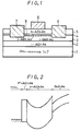
- Figure 1 illustrates a previously proposed MES gate type HEMT of AlInAs/GaInAs system.
- a semi-insulating InP substrate 1 On a semi-insulating InP substrate 1, there are epitaxially and sequentially grown an i-AlInAs layer 2, an i-GaInAs layer 3, an i-AlInAs layer 4 and an n-AlInAs layer 5.
- a metal gate electrode 6 is formed on the n-AlInAs layer 5, and metals are deposited and then alloyed on the n-AlInAs layer 5 at its portions corresponding to source and drain regions in ohmic contact to form a source electrode 7 and a drain electrode 8.
- a secondary electron gas channel 9 formed on the interface between the i-AlInAs layer 4 and the i-GaInAs layer 3 is represented by a dashed line.
- the height of a Schottky barrier in the gate portion is comparatively low, so that when a gate voltage is applied in the forward direction, the electrons in the channel 9 flow towards the gate electrode 6, increasing a so-called gate leakage current.
- the operating voltage range of this HEMT becomes narrow.
- a pn junction gate structure has been considered.
- the pn junction gate structure is formed in an AlInAs/GaInAs material system, it is natural that AlInAs or GaInAs is used as a p+ layer.
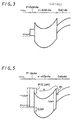
- Figure 2 shows an energy band structure of a p+-AlInAs layer
- Figure 3 shows an energy band structure of a p+-GaInAs layer. Neither of them, however, can prevent the gate leakage current effectively.
- a high electron mobility transistor comprising: a first semiconductive layer of relatively narrow band gap; and a second semiconductive layer of a relatively wide band gap; wherein a secondary electron gas channel is formed in said first semiconductive layer and on its interface opposing said second semiconductive layer; characterised by: a third semiconductive layer formed on said second semiconductive layer to become a gate portion, said third semiconductive layer forming a pn junction between it and said second semiconductive layer and having a conduction band the lower end of which is higher than a lower end of a conduction band of said second semiconductive layer to form a barrier.
- An embodiment of HEMT according to the invention includes a first semiconductive layer having a narrow band gap and a second semiconductive layer having a wide band gap, wherein a secondary electron gas channel is formed in the first semiconductive layer and on the interface between it and the second semiconductive layer.
- a third semiconductive layer is formed on the second semiconductive layer to form a pn junction between it and the second semiconductive layer.
- the third semiconductive layer has a conduction band the low end of which is higher than the lower end of a conduction band of the second semiconductive layer in an energy band structure to form a barrier.
- This third semiconductive layer becomes a gate portion.
- the third semiconductive layer has a metal gate electrode formed thereon and also there are formed source and drain electrodes made of metal deposited thereon at positions corresponding to source and drain regions in ohmic contact.
- the HEMT can suppress a gate leakage current by the barrier upon applying a gate voltage thereto in the forward direction and it can, therefore, be operated in a wide operating voltage range.
- an i-AlInAs layer 12 having a thickness of about 200 nm, a narrow band gap i-GaInAs layer 13 having a thickness of about 100 nm which becomes a channel forming layer, a wide band gap i-AlInAs layer 14 having a thickness of 5 nm, a wide band gap n-AlInAs layer 15 having a thickness of about 50 nm and having an impurity concentration of about 2 x 1018 cm ⁇ 3 and a p+-GaAs layer 16 having a thickness of about 20 nm and having an impurity concentration of about 5 x 10 18 cm ⁇ 3 which will become a gate portion.
- the GaAs layer 16 is selectively removed by a reactive ion etching (RIE) process, thus causing the p+GaAs layer 16 to be left only beneath the gate electrode 17.
- RIE reactive ion etching
- the RIE process is performed with the following conditions. If, for example, a gas of CCl2F2 (16 cc/min) and He(4 cc/min) is used and the RIE process is performed at a power of 50 W and under a pressure of 2.67 pascal, the etching rate is at 350 nm/min for the GaAs and the etching rate is at 5 nm/min for the AlInAs and hence the selection ratio becomes 70. Thus, the GaAs layer 16 only can be selectively etched away.
- metal for example, AuGe/Au
- a source electrode 18 and a drain electrode 19 each of which reaches the i-GaInAs layer 13, producing a desired pn junction gate type HEMT 20.
- a secondary electron gas channel 21 is formed on the heterojunction interface.
- Figure 5 is an energy band diagram of the thus made HEMT 20.
- the GaAs has substantially the same band gap as that of the AlInAs, the energy bands thereof are, however, not connected smoothly, causing a barrier ⁇ 1 of about 0.2 eV to occur in the conduction band.
- this barrier ⁇ 1 can prevent the electrons e of the channel 21 from flowing into the gate electrode 17.
- the lattice constant of the GaAs layer 16 is not coincident with the lattice constants of the GaInAs layer 13 and the AlInAs layers 12, 14 and 15 sequentially grown on the InP substrate 11, if the GaAs layer 16 is formed as a thin layer having a thickness of less than about 20 nm, that is, thickness of 10 nm to 20 nm, it is possible to form a monocrystalline layer of satisfactory quality.
- the GaAs layer 16 can be selectively etched away by the RIE method from the AlInAs layer 15, the HEMT 20 can easily be manufactured.
- the height of barrier ⁇ 2 on the heterojunction interface is twice or less, and the carrier density is twice.
- the mobility of electrons in the GaInAs layer is 1.5 times that in the GaAs layer, so that conductance of the GaInAs layer becomes 3 to 5 times as high as that of the GaAs layer.
- the GaAs layer is used as the p+ layer forming the gate portion, the GaAs layer may be replaced with the AlGaAs layer.
- the AlGaAs layer may prevent the gate leakage current more effectively than the GaAs layer does.
- the AlGaAs layer has selective etching properties inferior to the GaAs layer.
- the gate leakage current when the gate voltage is applied in the forward direction, the gate leakage current can be suppressed, so that a HEMT having a wide operating voltage range, can be manufactured.
Landscapes
- Junction Field-Effect Transistors (AREA)
Applications Claiming Priority (2)
| Application Number | Priority Date | Filing Date | Title |
|---|---|---|---|
| JP191635/87 | 1987-07-31 | ||
| JP62191635A JP2541228B2 (ja) | 1987-07-31 | 1987-07-31 | 高電子移動度トランジスタ |
Publications (1)
| Publication Number | Publication Date |
|---|---|
| EP0301862A2 true EP0301862A2 (fr) | 1989-02-01 |
Family
ID=16277934
Family Applications (1)
| Application Number | Title | Priority Date | Filing Date |
|---|---|---|---|
| EP88306966A Withdrawn EP0301862A2 (fr) | 1987-07-31 | 1988-07-28 | Transistors à haute mobilité électronique |
Country Status (3)
| Country | Link |
|---|---|
| EP (1) | EP0301862A2 (fr) |
| JP (1) | JP2541228B2 (fr) |
| KR (1) | KR890003045A (fr) |
Cited By (5)
| Publication number | Priority date | Publication date | Assignee | Title |
|---|---|---|---|---|
| GB2239557A (en) * | 1989-12-31 | 1991-07-03 | Samsung Electronics Co Ltd | High electron mobility transistors |
| US5144378A (en) * | 1990-03-06 | 1992-09-01 | Fujitsu Limited | High electron mobility transistor |
| WO2004010488A1 (fr) * | 2002-07-19 | 2004-01-29 | Sony Corporation | Dispositif semi-conducteur |
| US6876011B1 (en) | 2003-02-13 | 2005-04-05 | Mitsubishi Denki Kabushiki Kaisha | Semiconductor device |
| US9842905B2 (en) | 2011-07-15 | 2017-12-12 | Panasonic Intellectual Property Management Co., Ltd. | Semiconductor device and method for fabricating the same |
Families Citing this family (1)
| Publication number | Priority date | Publication date | Assignee | Title |
|---|---|---|---|---|
| KR100349884B1 (ko) * | 2001-02-26 | 2002-09-05 | 티씨제이이십일세기종합상사 주식회사 | 장신구 외주면의 문양 성형장치 |
-
1987
- 1987-07-31 JP JP62191635A patent/JP2541228B2/ja not_active Expired - Fee Related
-
1988
- 1988-07-25 KR KR1019880009311A patent/KR890003045A/ko not_active Abandoned
- 1988-07-28 EP EP88306966A patent/EP0301862A2/fr not_active Withdrawn
Cited By (7)
| Publication number | Priority date | Publication date | Assignee | Title |
|---|---|---|---|---|
| GB2239557A (en) * | 1989-12-31 | 1991-07-03 | Samsung Electronics Co Ltd | High electron mobility transistors |
| US5144378A (en) * | 1990-03-06 | 1992-09-01 | Fujitsu Limited | High electron mobility transistor |
| WO2004010488A1 (fr) * | 2002-07-19 | 2004-01-29 | Sony Corporation | Dispositif semi-conducteur |
| GB2406970A (en) * | 2002-07-19 | 2005-04-13 | Sony Corp | Semiconductor device |
| GB2406970B (en) * | 2002-07-19 | 2005-12-07 | Sony Corp | Semiconductor device |
| US6876011B1 (en) | 2003-02-13 | 2005-04-05 | Mitsubishi Denki Kabushiki Kaisha | Semiconductor device |
| US9842905B2 (en) | 2011-07-15 | 2017-12-12 | Panasonic Intellectual Property Management Co., Ltd. | Semiconductor device and method for fabricating the same |
Also Published As
| Publication number | Publication date |
|---|---|
| JP2541228B2 (ja) | 1996-10-09 |
| KR890003045A (ko) | 1989-04-12 |
| JPS6436080A (en) | 1989-02-07 |
Similar Documents
| Publication | Publication Date | Title |
|---|---|---|
| US6274893B1 (en) | Compound semiconductor device and method of manufacturing the same | |
| JP3716906B2 (ja) | 電界効果トランジスタ | |
| US6271547B1 (en) | Double recessed transistor with resistive layer | |
| US5701019A (en) | Semiconductor device having first and second stacked semiconductor layers, with electrical contact to the first semiconductor layer | |
| KR920003799B1 (ko) | 반도체 장치 | |
| EP1630860A2 (fr) | Transistors pseudomorphiques à haute mobilité d'électrons | |
| US20040169194A1 (en) | Semiconductor device | |
| EP0855748A1 (fr) | Transistor à effet de champ à hétérojonction et méthode de fabrication correspondante | |
| US6025613A (en) | Semiconductor device capable of reducing leak current and having excellent pinch-off characteristic and method of manufacturing the same | |
| US5939737A (en) | High-speed compound semiconductor device having a minimized parasitic capacitance and resistance | |
| EP0301862A2 (fr) | Transistors à haute mobilité électronique | |
| US5686740A (en) | Field effect transistor with recessed gate | |
| KR100548047B1 (ko) | 전계효과트랜지스터 | |
| JP3141935B2 (ja) | ヘテロ接合電界効果トランジスタ | |
| KR940010557B1 (ko) | 반도체장치 | |
| JPS61170071A (ja) | 化合物半導体を用いた接合ゲ−ト型電界効果トランジスタ | |
| US6410946B1 (en) | Semiconductor device with source and drain electrodes in ohmic contact with a semiconductor layer | |
| JP2003045898A (ja) | 半導体装置およびその製造方法 | |
| JP2695832B2 (ja) | ヘテロ接合型電界効果トランジスタ | |
| JP3077653B2 (ja) | 電界効果トランジスタ及びその製造方法 | |
| JP2668418B2 (ja) | 半導体装置 | |
| JPH06232168A (ja) | 電界効果トランジスタおよびその製造方法 | |
| EP0486063A2 (fr) | Transistor à effet de champ | |
| JPH05235056A (ja) | 半導体装置及びその製造方法 | |
| JPH05291306A (ja) | ヘテロ接合型電界効果トランジスタの素子間分離方法 |
Legal Events
| Date | Code | Title | Description |
|---|---|---|---|
| PUAI | Public reference made under article 153(3) epc to a published international application that has entered the european phase |
Free format text: ORIGINAL CODE: 0009012 |
|
| AK | Designated contracting states |
Kind code of ref document: A2 Designated state(s): DE FR GB NL |
|
| STAA | Information on the status of an ep patent application or granted ep patent |
Free format text: STATUS: THE APPLICATION HAS BEEN WITHDRAWN |
|
| 18W | Application withdrawn |
Withdrawal date: 19890920 |
|
| R18W | Application withdrawn (corrected) |
Effective date: 19890920 |