EP0303061A2 - Prozess zur Ausbildung eines planarisierten, mit Metall überzogenen Polysilizium-Gatter-FET - Google Patents
Prozess zur Ausbildung eines planarisierten, mit Metall überzogenen Polysilizium-Gatter-FET Download PDFInfo
- Publication number
- EP0303061A2 EP0303061A2 EP88111163A EP88111163A EP0303061A2 EP 0303061 A2 EP0303061 A2 EP 0303061A2 EP 88111163 A EP88111163 A EP 88111163A EP 88111163 A EP88111163 A EP 88111163A EP 0303061 A2 EP0303061 A2 EP 0303061A2
- Authority
- EP
- European Patent Office
- Prior art keywords
- layer
- substrate
- gate
- insulating layer
- regions
- Prior art date
- Legal status (The legal status is an assumption and is not a legal conclusion. Google has not performed a legal analysis and makes no representation as to the accuracy of the status listed.)
- Granted
Links
Images

Classifications
-
- H—ELECTRICITY
- H10—SEMICONDUCTOR DEVICES; ELECTRIC SOLID-STATE DEVICES NOT OTHERWISE PROVIDED FOR
- H10D—INORGANIC ELECTRIC SEMICONDUCTOR DEVICES
- H10D30/00—Field-effect transistors [FET]
- H10D30/01—Manufacture or treatment
- H10D30/021—Manufacture or treatment of FETs having insulated gates [IGFET]
- H10D30/0223—Manufacture or treatment of FETs having insulated gates [IGFET] having source and drain regions or source and drain extensions self-aligned to sides of the gate
-
- H—ELECTRICITY
- H10—SEMICONDUCTOR DEVICES; ELECTRIC SOLID-STATE DEVICES NOT OTHERWISE PROVIDED FOR
- H10D—INORGANIC ELECTRIC SEMICONDUCTOR DEVICES
- H10D30/00—Field-effect transistors [FET]
- H10D30/01—Manufacture or treatment
- H10D30/021—Manufacture or treatment of FETs having insulated gates [IGFET]
- H10D30/0212—Manufacture or treatment of FETs having insulated gates [IGFET] using self-aligned silicidation
-
- H—ELECTRICITY
- H10—SEMICONDUCTOR DEVICES; ELECTRIC SOLID-STATE DEVICES NOT OTHERWISE PROVIDED FOR
- H10D—INORGANIC ELECTRIC SEMICONDUCTOR DEVICES
- H10D64/00—Electrodes of devices having potential barriers
- H10D64/01—Manufacture or treatment
- H10D64/013—Manufacture or treatment of electrodes having a conductor capacitively coupled to a semiconductor by an insulator
- H10D64/01302—Manufacture or treatment of electrodes having a conductor capacitively coupled to a semiconductor by an insulator the insulator being formed after the semiconductor body, the semiconductor being silicon
- H10D64/01304—Manufacture or treatment of electrodes having a conductor capacitively coupled to a semiconductor by an insulator the insulator being formed after the semiconductor body, the semiconductor being silicon characterised by the conductor
- H10D64/01306—Manufacture or treatment of electrodes having a conductor capacitively coupled to a semiconductor by an insulator the insulator being formed after the semiconductor body, the semiconductor being silicon characterised by the conductor the conductor comprising a layer of silicon contacting the insulator, e.g. polysilicon
- H10D64/01308—Manufacture or treatment of electrodes having a conductor capacitively coupled to a semiconductor by an insulator the insulator being formed after the semiconductor body, the semiconductor being silicon characterised by the conductor the conductor comprising a layer of silicon contacting the insulator, e.g. polysilicon the conductor further comprising a non-elemental silicon additional conductive layer, e.g. a metal silicide layer formed by the reaction of silicon with an implanted metal
- H10D64/01312—Manufacture or treatment of electrodes having a conductor capacitively coupled to a semiconductor by an insulator the insulator being formed after the semiconductor body, the semiconductor being silicon characterised by the conductor the conductor comprising a layer of silicon contacting the insulator, e.g. polysilicon the conductor further comprising a non-elemental silicon additional conductive layer, e.g. a metal silicide layer formed by the reaction of silicon with an implanted metal the additional layer comprising a metal or metal silicide formed by deposition, i.e. without a silicidation reaction, e.g. sputter deposition
-
- H—ELECTRICITY
- H10—SEMICONDUCTOR DEVICES; ELECTRIC SOLID-STATE DEVICES NOT OTHERWISE PROVIDED FOR
- H10D—INORGANIC ELECTRIC SEMICONDUCTOR DEVICES
- H10D64/00—Electrodes of devices having potential barriers
- H10D64/20—Electrodes characterised by their shapes, relative sizes or dispositions
- H10D64/23—Electrodes carrying the current to be rectified, amplified, oscillated or switched, e.g. sources, drains, anodes or cathodes
- H10D64/251—Source or drain electrodes for field-effect devices
- H10D64/258—Source or drain electrodes for field-effect devices characterised by the relative positions of the source or drain electrodes with respect to the gate electrode
- H10D64/259—Source or drain electrodes being self-aligned with the gate electrode and having bottom surfaces higher than the interface between the channel and the gate dielectric
-
- H—ELECTRICITY
- H10—SEMICONDUCTOR DEVICES; ELECTRIC SOLID-STATE DEVICES NOT OTHERWISE PROVIDED FOR
- H10P—GENERIC PROCESSES OR APPARATUS FOR THE MANUFACTURE OR TREATMENT OF DEVICES COVERED BY CLASS H10
- H10P32/00—Diffusion of dopants within, into or out of wafers, substrates or parts of devices
- H10P32/10—Diffusion of dopants within, into or out of semiconductor bodies or layers
- H10P32/14—Diffusion of dopants within, into or out of semiconductor bodies or layers within a single semiconductor body or layer in a solid phase; between different semiconductor bodies or layers, both in a solid phase
- H10P32/1408—Diffusion of dopants within, into or out of semiconductor bodies or layers within a single semiconductor body or layer in a solid phase; between different semiconductor bodies or layers, both in a solid phase from or through or into an external applied layer, e.g. photoresist or nitride layers
- H10P32/1414—Diffusion of dopants within, into or out of semiconductor bodies or layers within a single semiconductor body or layer in a solid phase; between different semiconductor bodies or layers, both in a solid phase from or through or into an external applied layer, e.g. photoresist or nitride layers the applied layer being silicon, silicide or SIPOS, e.g. polysilicon or porous silicon
-
- H—ELECTRICITY
- H10—SEMICONDUCTOR DEVICES; ELECTRIC SOLID-STATE DEVICES NOT OTHERWISE PROVIDED FOR
- H10P—GENERIC PROCESSES OR APPARATUS FOR THE MANUFACTURE OR TREATMENT OF DEVICES COVERED BY CLASS H10
- H10P32/00—Diffusion of dopants within, into or out of wafers, substrates or parts of devices
- H10P32/10—Diffusion of dopants within, into or out of semiconductor bodies or layers
- H10P32/17—Diffusion of dopants within, into or out of semiconductor bodies or layers characterised by the semiconductor material
- H10P32/171—Diffusion of dopants within, into or out of semiconductor bodies or layers characterised by the semiconductor material being group IV material
-
- H—ELECTRICITY
- H10—SEMICONDUCTOR DEVICES; ELECTRIC SOLID-STATE DEVICES NOT OTHERWISE PROVIDED FOR
- H10D—INORGANIC ELECTRIC SEMICONDUCTOR DEVICES
- H10D64/00—Electrodes of devices having potential barriers
- H10D64/01—Manufacture or treatment
- H10D64/017—Manufacture or treatment using dummy gates in processes wherein at least parts of the final gates are self-aligned to the dummy gates, i.e. replacement gate processes
Definitions
- the present invention relates to reducing the sheet resistance of the source, gate and drain electrodes of an FET device.
- This conductive line typically forms the control electrode of at least one of the devices that comprise a given memory cell.
- the word line provides the gate electrode of the transistor.
- Another method of reducing sheet resistance is to use refractory metal silicides that are formed on top of (i.e., "strap") a polysilicon gate.
- a silicide layer is formed simultaneously over the gate electrode and the source/drain diffusion regions of an FET device. More specifically, after a polysilicon gate electrode has been defined on a substrate, ions are implanted to define the source/drain diffusion regions. Then an oxide layer is deposited and etched so that the sidewalls of the polysilicon gate electrode are covered with oxide.
- a refractory metal layer (the patent utilizes tantalum) is deposited on the substrate, and a heat cycle is carried out to form tantalum silicide in those portions of the tantalum disposed on exposed silicon. Note that the oxide disposed on the sidewalls of the polysilicon gate electrode prevent the silicide formed on the upper surface of the gate electrode from being connected to the silicide formed on the source/drain regions.
- the general simultaneous gate and source/drain silicide formation process as exemplified by the Baudrant et al patent suffers from several shortcomings.
- a recent trend in the semiconductor industry is to decrease the depth of the source/drain diffusion regions to less than 0.5 microns. These so-called “shallow junctions" are more resistant to punchthrough defects as the channel length of FET's is decreased below the one micron barrier. If a refractory metal is deposited over the shallow junctions to form a silicide thereon, the amount of junction silicon consumed during the silicide reaction may substantially degrade the characteristics of these shallow junction regions. In the prior art, this problem has been addressed by incorporating extra silicon at the shallow junction surface prior to refractory metal deposition.
- the oxide layer above the source/drain diffusion regions is removed, and a second layer of titanium is deposited on the substrate.
- the earlier-formed titanium silicide gate electrode will increase in thickness.
- a thick titanium silicide layer is formed on the gate electrode, and a thin titanium silicide layer is formed over the source/drain regions.
- the present inventors have investigated various methods of reducing the sheet resistance of the gate electrode below that obtained by refractory metal silicides.
- Tungsten silicide provides a resistivity of approximately 50 micro ohms-cm.
- a tungsten layer has a resistivity of approximately 10 micro ohms-cm
- an aluminum layer has a resistivity on the order of 3 micro ohms-cm.
- the inventors considered modifying an approach similar to the Lynch et al patent by replacing the silicide gate formation step with depositing either tungsten or aluminum. However, this modification would not achieve the intended result.
- tungsten were to be deposited on top of a layer of polysilicon, the layers would react to form a silicide during the subsequent implant drive-in and source/drain silicide formation steps. This would greatly increase the sheet resistance of the gate electrode by forming tungsten silicide (as opposed to pure tungsten). Similarly, the physical/electrical qualities of an aluminum layer (or an aluminum alloy such as aluminum/silicon) would substantially degrade when exposed to these high processing temperatures.
- CMOS circuits utilize so-called “dual work function" gate electrodes.
- the polysilicon gates for the n-channel and p-channel devices are doped with P-type and N-type dopants, respectively, in order to achieve an enhanced p-channel device characteristic. If these differentially-doped polysilicon gate electrodes are covered with a refractory metal layer for subsequent silicide formation, the polysilicon dopants may intermix (due to the high dopant diffusively in refractory metal silicides) to destroy the above dual-work function advantages.
- the invention as claimed solves the problem of providing the lowest possible sheet resistance metal-strapped polysilicon gate electrode for an FET device having a planar upper surface without causing intermixing of dual work function dopants and of providing the shallowest possible source/drain regions for the FET device while also providing low sheet resistance silicide electrodes for the source/drain regions.
- a gate stack is defined on an exposed surface of a semiconductor substrate.
- the gate stack includes a gate mask disposed on a patterned polysilicon layer.
- first and second shallow diffusion regions are formed having first and second silicide electrodes disposed on them.
- An insulating layer is then deposited on the substrate.
- the insulating layer has a thickness that is substantially equal to that of said gate stack.
- the insulator layer is planarized so as to expose an upper surface of said gate mask and the gate mask is removed to define an aperture in the insulating layer that exposes the polysilicon layer.
- N-type and p-type dopants are introduced to selected regions of the exposed polysilicon to define dual work function gates, and a low sheet resistance conductive material is deposited on the substrate to at least partially fill the apertures in said insulating layer so as to form a gate electrode of said FET that is relatively co-planar with the planarized insulating layer.
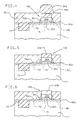
- layers of polysilicon 30 and silicon nitride 40 are formed on a substrate 1.
- the substrate 1 is a P+ type, ⁇ 100> monocrystalline silicon wafer having an isolation region 10 formed therein.
- a thin p-type epitaxial layer is grown on the p+ substrate, and an n-well is formed in selected portions of the epitaxial layer.
- the epi layer and the n-well are not shown solely for the sake of simplicity.
- the isolation region 10 could be conventional semi-recessed oxide isolation (S-ROX) structures.
- S-ROX semi-recessed oxide isolation
- Diffusion region 15 is then formed by simply implanting dopant into the substrate after the isolation region 10 is formed. Diffusion region 15 is formed by implanting or diffusing an n-type dopant. The purpose of region 15 is to control the threshold voltages of the FET devices to be subsequently formed.
- dielectric layer 20 is formed on the exposed surface of the substrate.
- dielectric layer 20 is a 10 nm thick layer of silicon oxide.
- other structures having suitable dielectric properties e.g. silicon oxynitride, silicon nitride, or a plurality of silicon nitride and silicon oxide layers
- a 200 nm thick layer of p-type polycrystalline silicon 30 is then deposited on the dielectric layer 20 using conventional techniques, and a 250 nm thick layer of CVD silicon nitride 40 is formed on the polysilicon layer 30, also using conventional techniques.
- a layer of photosensitive polymer e.g., a novolak-based photoresist
- a photomask 50 having substantially vertical sidewalls.
- the exposed portions of silicon nitride layer 40 and polysilicon layer 30 are then sequentially etched in a directional mode to define a gate stack 100 that includes a silicon nitride portion 40A and a polysilicon portion 30A.
- the silicon nitride layer can be patterned by exposure to a CF4/O2 plasma and the polysilicon layer 30 can be patterned by exposure to an HCl/Cl2 gaseous plasma.
- the silicon nitride portion 40A defines a masking structure above the polysilicon gate electrode 30A.
- sidewall spacers 60 are formed on the exposed sides of polysilicon portion 30A.
- the sidewall spacers 60 can be formed using one or two methods.
- the first method is to simply oxidize the exposed surfaces of polysilicon portion 30A.
- the overlying silicon nitride masking structure 40A prevents the upper surface of polysilicon portion 30A from being oxidized during this step.
- the preferred method is to deposit a layer of oxide over the entire structure, and directionally etch the deposited layer so that it is removed from the horizontal surfaces of the substrate.
- gate dielectric 20A exposed portions of the underlying oxide layer 20 are also removed to define gate dielectric 20A.
- the source and drain regions 70, 80 are formed, and silicide electrodes 70A, 80A are formed thereon, respectively.
- the diffusion regions and silicide electrodes can be formed using one of several techniques.
- One technique is to simply implant the dopant ions to define the diffusion regions using the gate stack 100 as an implantation mask, deposit a refractory metal such as cobalt or titanium over the substrate, and sinter the structure to form CoSi2 or TiSi2 over the junction regions.
- a refractory metal such as cobalt or titanium
- the silicon nitride 40A and the sidewalls 60 prevent the refractory metal from combining with polysilicon 30A to form a gate silicide.
- a first alternative is to first grow epitaxial silicon over the exposed silicon regions in order to reduce the amount of silicon consumed during the silicide reaction, and then to carry out the above-described implant, refractory metal deposition and anneal steps. This first alternative would be employed when shallow junctions are desired.
- Another alternative is to deposit the refractory metal (e.g.
- Cobalt heat treat the substrate for an amount of time sufficient to form a metal-rich silicide (by carrying out the anneal at temperatures or for times that are insufficient to form a silicon-rich silicide), remove the refractory metal without removing the metal-rich silicide, implant ions into the metal-rich silicide, and anneal the substrate in order to drive the dopants out of the metal-rich silicide to define shallow source/drain junction regions while converting the metal-rich silicide into silicon-rich silicide.
- This latter alternative is preferred, in that it is compatible with shallow junctions without necessitating selective epitaxial silicon growth.
- the key factor is that the process is carried out in the presence of a masking structure atop the polysilicon gate.
- the silicide formation and dopant diffusion steps which are typically carried out at temperatures ranging between 800°C-1000°C, are performed prior to complete formation of the gate electrode of the FET.
- the substrate is then covered with a thick conformal layer 90, preferably of silicon dioxide.
- the thickness of the deposited conformal layer 90 should be slightly less than the gate stack thickness (i.e., approximately 450 nm). This thickness differential is needed to account for variations in the topography across the wafer surface.
- the isolation region 10 is constructed to have a surface that is relatively co-planar with the upper surface of substrate 1, in practice the surface of isolation region 10 may extend above the surface of substrate 1.
- a portion 90A of conformal layer 90 extends above the upper surface the gate stack 100. The thickness differential between conformal layer 90 and gate stack 100 is particularly important in removing portion 90A by polishing as described below.
- the surface of conformal layer 90 is then planarized so as to remove portion 90A extending above the upper surface of the gate stack 100.
- a preferred method of planarizing the conformal layer 90 is to subject the wafer to a mechanical polishing procedure in the presence of an abrasive slurry. More specifically, a slurry commercially available from Cabot Corp. under the tradename "Cabot SCO1" is supplied to a Strasbaugh wafer polishing tool having a Suba IV perforated abrasive pad held at a pressure of 0,41 - 0,55 mbar. It has been found that carrying out this procedure for approximately four minutes is sufficient to remove portion 90A and to planarize the bulk film 90.
- the polishing pad contacts the upper surface of the remainder of the conformal layer. It has been found that the frictional force experienced by the polishing pad greatly increases as the polishing pad contacts the bulk conformal layer surface. The force experienced by the pad can be monitored, such that the polishing procedure can be stopped at this point or continued for a discrete amount of time afterward.
- the upper surface of the silicon nitride masking structure is approximately co-planar with, and is exposed by, the remaining portions of conformal layer 90.
- planarization method consists of coating the surface of conformal oxide layer 90 with a layer of photoresist, and exposing the substrate to an etchant that will remove the photoresist and the underlaying oxide at substantially the same rate. Since the photoresist is a non-conformal layer, its planar upper surface is simply replicated in the oxide layer. This method is discussed in the above-mentioned U.S. Patent Application S.N. 927,623.
- silicon nitride masking structure is removed to expose the underlaying portion of polysilicon gate 30A.
- silicon nitride can be removed without appreciably attacking silicon dioxide or polysilicon by exposure to H3PO4 solvent at a temperature of 165°C.
- a block mask is deposited over the n-channel devices, and the exposed polysilicon within the exposed vias is implanted with p-type impurity. Then a second block mask (the complement of the first block mask) is defined, and the exposed polysilicon is implanted with an n-type dopant.
- the dual work-function implants are carried out after the polysilicon has been patterned and after the silicon nitride mask is removed. If the implants were carried out before the polysilicon was patterned, the resulting n and p doped polysilicon regions would subsequently etch at different rates. If the implants were carried out after patterning, the high implant energy required to penetrate the silicon nitride mask may result in the undesired doping other structures.
- metal 30B is deposited and defined (as needed) to strap the FET gate electrode. It is preferred to form metal layer 30B of selective tungsten. Under conditions discussed in an article by Foster et al, entitled “Selective Tungsten Deposition In a Varian/Torrex Cold Wall CVD Reactor," Tungsten and Other Refractory Metals for VLSI II , (Conference Proceedings, Nov. 12-14, 1986), pp. 147-155, tungsten can be chemically vapor deposited such that it only grows on silicon. Thus, tungsten can be grown to fill the space that was previously defined by nitride mask 40A. Such a procedure eliminates the need to etch back the deposited metal.
- the process of the invention provides an FET device having a low sheet resistance gate electrode as well as silicide source and drain electrodes.
- the tungsten component of the tungsten-polysilicon composite gate electrode is not introduced until after the hot process steps associated with the source/drain dopant diffusion and silicide formation steps are carried out.
- tungsten which normally forms a silicide with silicon at a temperature of approximately 600°C
- Another advantage of the invention is that the final structure is planar as between the final gate electrode and the surrounding conformal oxide layer.
- a passivating oxide layer is subsequently deposited on the formed device, there is no need to reflow the passivation layer so as to form a planar upper surface.
- this reflow step is carried out at a temperature of 800-1000°C.
- the invention further reduced the risk of silicide gate formation by eliminating a subsequent hot process step that is normally carried out in conventional device fabrication processes, while also providing an FET device that is more compatible with multiple levels of metal.
- Another advantage of the present invention is that the metal on top of the polysilicon does not allow intermixing of the dual work function polysilicon dopants.
- the invention provides a low sheet resistant gate electrode that is compatible with dual work function CMOS polysilicon gate technology.
Landscapes
- Electrodes Of Semiconductors (AREA)
- Insulated Gate Type Field-Effect Transistor (AREA)
- Internal Circuitry In Semiconductor Integrated Circuit Devices (AREA)
Applications Claiming Priority (2)
| Application Number | Priority Date | Filing Date | Title |
|---|---|---|---|
| US07/084,719 US4755478A (en) | 1987-08-13 | 1987-08-13 | Method of forming metal-strapped polysilicon gate electrode for FET device |
| US84719 | 1987-08-13 |
Publications (3)
| Publication Number | Publication Date |
|---|---|
| EP0303061A2 true EP0303061A2 (de) | 1989-02-15 |
| EP0303061A3 EP0303061A3 (en) | 1989-04-26 |
| EP0303061B1 EP0303061B1 (de) | 1992-05-27 |
Family
ID=22186794
Family Applications (1)
| Application Number | Title | Priority Date | Filing Date |
|---|---|---|---|
| EP88111163A Expired EP0303061B1 (de) | 1987-08-13 | 1988-07-12 | Prozess zur Ausbildung eines planarisierten, mit Metall überzogenen Polysilizium-Gatter-FET |
Country Status (4)
| Country | Link |
|---|---|
| US (1) | US4755478A (de) |
| EP (1) | EP0303061B1 (de) |
| JP (1) | JPH0760899B2 (de) |
| DE (1) | DE3871457D1 (de) |
Cited By (12)
| Publication number | Priority date | Publication date | Assignee | Title |
|---|---|---|---|---|
| EP0601951A3 (de) * | 1992-12-11 | 1995-01-04 | Ibm | Verfahren zum Verbessern des Gateschichtwiderstands einer Fieldeffekttransitorvorrichtung. |
| US5830797A (en) * | 1996-06-20 | 1998-11-03 | Cypress Semiconductor Corporation | Interconnect methods and apparatus |
| US5911887A (en) * | 1996-07-19 | 1999-06-15 | Cypress Semiconductor Corporation | Method of etching a bond pad |
| US5972124A (en) * | 1998-08-31 | 1999-10-26 | Advanced Micro Devices, Inc. | Method for cleaning a surface of a dielectric material |
| US6004874A (en) * | 1996-06-26 | 1999-12-21 | Cypress Semiconductor Corporation | Method for forming an interconnect |
| US6091129A (en) * | 1996-06-19 | 2000-07-18 | Cypress Semiconductor Corporation | Self-aligned trench isolated structure |
| US6143663A (en) * | 1998-01-22 | 2000-11-07 | Cypress Semiconductor Corporation | Employing deionized water and an abrasive surface to polish a semiconductor topography |
| EP0991114A3 (de) * | 1998-10-01 | 2000-12-27 | Chartered Semiconductor Manufacturing Pte Ltd. | Metall- und Polysiliziumgate mit ultraniedrigem Schichtwiderstand für Anwendungen in submikronischen CMOS |
| US6171180B1 (en) | 1998-03-31 | 2001-01-09 | Cypress Semiconductor Corporation | Planarizing a trench dielectric having an upper surface within a trench spaced below an adjacent polish stop surface |
| US6200896B1 (en) | 1998-01-22 | 2001-03-13 | Cypress Semiconductor Corporation | Employing an acidic liquid and an abrasive surface to polish a semiconductor topography |
| US6232231B1 (en) | 1998-08-31 | 2001-05-15 | Cypress Semiconductor Corporation | Planarized semiconductor interconnect topography and method for polishing a metal layer to form interconnect |
| WO2000075967A3 (en) * | 1999-06-03 | 2001-07-05 | Advanced Micro Devices Inc | Method for fabrication of a low resistivity mosfet gate with thick metal silicide on polysilicon |
Families Citing this family (58)
| Publication number | Priority date | Publication date | Assignee | Title |
|---|---|---|---|---|
| US4965218A (en) * | 1985-10-21 | 1990-10-23 | Itt Corporation | Self-aligned gate realignment employing planarizing overetch |
| US5028555A (en) * | 1987-12-02 | 1991-07-02 | Advanced Micro Devices, Inc. | Self-aligned semiconductor devices |
| NL8800222A (nl) * | 1988-01-29 | 1989-08-16 | Philips Nv | Werkwijze voor het vervaardigen van een halfgeleiderinrichting waarbij op zelfregistrerende wijze metaalsilicide wordt aangebracht. |
| US4877755A (en) * | 1988-05-31 | 1989-10-31 | Texas Instruments Incorporated | Method of forming silicides having different thicknesses |
| JPH02105466A (ja) * | 1988-10-13 | 1990-04-18 | Nec Corp | 絶縁ゲート型電界効果トランジスタの製造方法 |
| US4908332A (en) * | 1989-05-04 | 1990-03-13 | Industrial Technology Research Institute | Process for making metal-polysilicon double-layered gate |
| US5153145A (en) * | 1989-10-17 | 1992-10-06 | At&T Bell Laboratories | Fet with gate spacer |
| DE69109366T2 (de) * | 1990-05-31 | 1995-10-19 | Canon Kk | Verfahren zur Herstellung einer Halbleiteranordnung mit Gatestruktur. |
| US5034348A (en) * | 1990-08-16 | 1991-07-23 | International Business Machines Corp. | Process for forming refractory metal silicide layers of different thicknesses in an integrated circuit |
| US5086017A (en) * | 1991-03-21 | 1992-02-04 | Industrial Technology Research Institute | Self aligned silicide process for gate/runner without extra masking |
| US6964890B1 (en) | 1992-03-17 | 2005-11-15 | Semiconductor Energy Laboratory Co., Ltd. | Semiconductor device and method for forming the same |
| US6624477B1 (en) | 1992-10-09 | 2003-09-23 | Semiconductor Energy Laboratory Co., Ltd. | Semiconductor device and method for manufacturing the same |
| TW232751B (en) * | 1992-10-09 | 1994-10-21 | Semiconductor Energy Res Co Ltd | Semiconductor device and method for forming the same |
| US5275973A (en) * | 1993-03-01 | 1994-01-04 | Motorola, Inc. | Method for forming metallization in an integrated circuit |
| JPH07135317A (ja) * | 1993-04-22 | 1995-05-23 | Texas Instr Inc <Ti> | 自己整合型シリサイドゲート |
| US5322809A (en) * | 1993-05-11 | 1994-06-21 | Texas Instruments Incorporated | Self-aligned silicide process |
| JPH0730125A (ja) | 1993-07-07 | 1995-01-31 | Semiconductor Energy Lab Co Ltd | 半導体装置およびその作製方法 |
| US5395799A (en) * | 1993-10-04 | 1995-03-07 | At&T Corp. | Method of fabricating semiconductor devices having electrodes comprising layers of doped tungsten disilicide |
| US5480837A (en) * | 1994-06-27 | 1996-01-02 | Industrial Technology Research Institute | Process of making an integrated circuit having a planar conductive layer |
| US5814545A (en) * | 1995-10-02 | 1998-09-29 | Motorola, Inc. | Semiconductor device having a phosphorus doped PECVD film and a method of manufacture |
| US6289396B1 (en) | 1995-11-21 | 2001-09-11 | Diamond Multimedia Systems, Inc. | Dynamic programmable mode switching device driver architecture |
| US6393495B1 (en) | 1995-11-21 | 2002-05-21 | Diamond Multimedia Systems, Inc. | Modular virtualizing device driver architecture |
| US6009476A (en) * | 1995-11-21 | 1999-12-28 | Diamond Multimedia Systems, Inc. | Device driver architecture supporting emulation environment |
| US5752032A (en) * | 1995-11-21 | 1998-05-12 | Diamond Multimedia Systems, Inc. | Adaptive device driver using controller hardware sub-element identifier |
| US5770490A (en) * | 1996-08-29 | 1998-06-23 | International Business Machines Corporation | Method for producing dual work function CMOS device |
| US6028339A (en) * | 1996-08-29 | 2000-02-22 | International Business Machines Corporation | Dual work function CMOS device |
| US5985768A (en) * | 1997-04-30 | 1999-11-16 | International Business Machines Corporation | Method of forming a semiconductor |
| JP3389075B2 (ja) | 1997-10-01 | 2003-03-24 | 株式会社東芝 | 半導体装置の製造方法 |
| JP3199015B2 (ja) | 1998-02-04 | 2001-08-13 | 日本電気株式会社 | 半導体装置及びその製造方法 |
| US7804115B2 (en) * | 1998-02-25 | 2010-09-28 | Micron Technology, Inc. | Semiconductor constructions having antireflective portions |
| US6274292B1 (en) | 1998-02-25 | 2001-08-14 | Micron Technology, Inc. | Semiconductor processing methods |
| US6281100B1 (en) | 1998-09-03 | 2001-08-28 | Micron Technology, Inc. | Semiconductor processing methods |
| US6268282B1 (en) | 1998-09-03 | 2001-07-31 | Micron Technology, Inc. | Semiconductor processing methods of forming and utilizing antireflective material layers, and methods of forming transistor gate stacks |
| US6077750A (en) * | 1998-10-27 | 2000-06-20 | Lg Semicon Co., Ltd. | Method for forming epitaxial Co self-align silicide for semiconductor device |
| US6828683B2 (en) | 1998-12-23 | 2004-12-07 | Micron Technology, Inc. | Semiconductor devices, and semiconductor processing methods |
| US7235499B1 (en) * | 1999-01-20 | 2007-06-26 | Micron Technology, Inc. | Semiconductor processing methods |
| TW425612B (en) * | 1999-06-10 | 2001-03-11 | Nanya Technology Corp | Method for producing gate of embedded DRAM |
| US7067414B1 (en) | 1999-09-01 | 2006-06-27 | Micron Technology, Inc. | Low k interlevel dielectric layer fabrication methods |
| US6440860B1 (en) * | 2000-01-18 | 2002-08-27 | Micron Technology, Inc. | Semiconductor processing methods of transferring patterns from patterned photoresists to materials, and structures comprising silicon nitride |
| US6504210B1 (en) | 2000-06-23 | 2003-01-07 | International Business Machines Corporation | Fully encapsulated damascene gates for Gigabit DRAMs |
| KR100380348B1 (ko) * | 2001-01-11 | 2003-04-11 | 삼성전자주식회사 | 자기 정렬 콘택의 게이트 스페이서를 형성하는 방법 |
| US6703688B1 (en) | 2001-03-02 | 2004-03-09 | Amberwave Systems Corporation | Relaxed silicon germanium platform for high speed CMOS electronics and high speed analog circuits |
| US6830976B2 (en) | 2001-03-02 | 2004-12-14 | Amberwave Systems Corproation | Relaxed silicon germanium platform for high speed CMOS electronics and high speed analog circuits |
| US6969684B1 (en) | 2001-04-30 | 2005-11-29 | Cypress Semiconductor Corp. | Method of making a planarized semiconductor structure |
| US6459562B1 (en) * | 2001-05-22 | 2002-10-01 | Conexant Systems, Inc. | High density metal insulator metal capacitors |
| US6888198B1 (en) | 2001-06-04 | 2005-05-03 | Advanced Micro Devices, Inc. | Straddled gate FDSOI device |
| US6630720B1 (en) | 2001-12-26 | 2003-10-07 | Advanced Micro Devices, Inc. | Asymmetric semiconductor device having dual work function gate and method of fabrication |
| US6830975B2 (en) * | 2002-01-31 | 2004-12-14 | Micron Technology, Inc. | Method of forming field effect transistor comprising at least one of a conductive metal or metal compound in electrical connection with transistor gate semiconductor material |
| US6828678B1 (en) | 2002-03-29 | 2004-12-07 | Silicon Magnetic Systems | Semiconductor topography with a fill material arranged within a plurality of valleys associated with the surface roughness of the metal layer |
| JP3970682B2 (ja) * | 2002-05-17 | 2007-09-05 | 株式会社ルネサステクノロジ | 半導体装置の製造方法 |
| US6586808B1 (en) | 2002-06-06 | 2003-07-01 | Advanced Micro Devices, Inc. | Semiconductor device having multi-work function gate electrode and multi-segment gate dielectric |
| US7615829B2 (en) | 2002-06-07 | 2009-11-10 | Amberwave Systems Corporation | Elevated source and drain elements for strained-channel heterojuntion field-effect transistors |
| WO2003105206A1 (en) | 2002-06-10 | 2003-12-18 | Amberwave Systems Corporation | Growing source and drain elements by selecive epitaxy |
| US6982474B2 (en) | 2002-06-25 | 2006-01-03 | Amberwave Systems Corporation | Reacted conductive gate electrodes |
| CN100437970C (zh) | 2003-03-07 | 2008-11-26 | 琥珀波系统公司 | 一种结构及用于形成半导体结构的方法 |
| US6924184B2 (en) * | 2003-03-21 | 2005-08-02 | Freescale Semiconductor, Inc. | Semiconductor device and method for forming a semiconductor device using post gate stack planarization |
| KR100595899B1 (ko) * | 2003-12-31 | 2006-06-30 | 동부일렉트로닉스 주식회사 | 이미지 센서 및 그 제조방법 |
| US8546252B2 (en) * | 2009-10-05 | 2013-10-01 | International Business Machines Corporation | Metal gate FET having reduced threshold voltage roll-off |
Family Cites Families (14)
| Publication number | Priority date | Publication date | Assignee | Title |
|---|---|---|---|---|
| US3994758A (en) * | 1973-03-19 | 1976-11-30 | Nippon Electric Company, Ltd. | Method of manufacturing a semiconductor device having closely spaced electrodes by perpendicular projection |
| US4441247A (en) * | 1981-06-29 | 1984-04-10 | Intel Corporation | Method of making MOS device by forming self-aligned polysilicon and tungsten composite gate |
| JPS584924A (ja) * | 1981-07-01 | 1983-01-12 | Hitachi Ltd | 半導体装置の電極形成方法 |
| JPS5941870A (ja) * | 1982-08-25 | 1984-03-08 | Toshiba Corp | 半導体装置の製造方法 |
| DE3242113A1 (de) * | 1982-11-13 | 1984-05-24 | Ibm Deutschland Gmbh, 7000 Stuttgart | Verfahren zur herstellung einer duennen dielektrischen isolation in einem siliciumhalbleiterkoerper |
| DE3304588A1 (de) * | 1983-02-10 | 1984-08-16 | Siemens AG, 1000 Berlin und 8000 München | Verfahren zum herstellen von mos-transistoren mit flachen source/drain-gebieten, kurzen kanallaengen und einer selbstjustierten, aus einem metallsilizid bestehenden kontaktierungsebene |
| US4453306A (en) * | 1983-05-27 | 1984-06-12 | At&T Bell Laboratories | Fabrication of FETs |
| FR2555365B1 (fr) * | 1983-11-22 | 1986-08-29 | Efcis | Procede de fabrication de circuit integre avec connexions de siliciure de tantale et circuit integre realise selon ce procede |
| US4470874A (en) * | 1983-12-15 | 1984-09-11 | International Business Machines Corporation | Planarization of multi-level interconnected metallization system |
| US4587718A (en) * | 1984-11-30 | 1986-05-13 | Texas Instruments Incorporated | Process for forming TiSi2 layers of differing thicknesses in a single integrated circuit |
| JPS61284963A (ja) * | 1985-06-10 | 1986-12-15 | Nippon Telegr & Teleph Corp <Ntt> | 半導体装置とその製造方法 |
| US4648175A (en) * | 1985-06-12 | 1987-03-10 | Ncr Corporation | Use of selectively deposited tungsten for contact formation and shunting metallization |
| US4707456A (en) * | 1985-09-18 | 1987-11-17 | Advanced Micro Devices, Inc. | Method of making a planar structure containing MOS and bipolar transistors |
| JPS62104078A (ja) * | 1985-10-31 | 1987-05-14 | Nec Corp | 半導体集積回路装置の製造方法 |
-
1987
- 1987-08-13 US US07/084,719 patent/US4755478A/en not_active Expired - Fee Related
-
1988
- 1988-06-06 JP JP63137585A patent/JPH0760899B2/ja not_active Expired - Lifetime
- 1988-07-12 DE DE8888111163T patent/DE3871457D1/de not_active Expired - Lifetime
- 1988-07-12 EP EP88111163A patent/EP0303061B1/de not_active Expired
Cited By (13)
| Publication number | Priority date | Publication date | Assignee | Title |
|---|---|---|---|---|
| EP0601951A3 (de) * | 1992-12-11 | 1995-01-04 | Ibm | Verfahren zum Verbessern des Gateschichtwiderstands einer Fieldeffekttransitorvorrichtung. |
| US6091129A (en) * | 1996-06-19 | 2000-07-18 | Cypress Semiconductor Corporation | Self-aligned trench isolated structure |
| US5830797A (en) * | 1996-06-20 | 1998-11-03 | Cypress Semiconductor Corporation | Interconnect methods and apparatus |
| US6004874A (en) * | 1996-06-26 | 1999-12-21 | Cypress Semiconductor Corporation | Method for forming an interconnect |
| US5911887A (en) * | 1996-07-19 | 1999-06-15 | Cypress Semiconductor Corporation | Method of etching a bond pad |
| US6200896B1 (en) | 1998-01-22 | 2001-03-13 | Cypress Semiconductor Corporation | Employing an acidic liquid and an abrasive surface to polish a semiconductor topography |
| US6143663A (en) * | 1998-01-22 | 2000-11-07 | Cypress Semiconductor Corporation | Employing deionized water and an abrasive surface to polish a semiconductor topography |
| US6171180B1 (en) | 1998-03-31 | 2001-01-09 | Cypress Semiconductor Corporation | Planarizing a trench dielectric having an upper surface within a trench spaced below an adjacent polish stop surface |
| US5972124A (en) * | 1998-08-31 | 1999-10-26 | Advanced Micro Devices, Inc. | Method for cleaning a surface of a dielectric material |
| US6232231B1 (en) | 1998-08-31 | 2001-05-15 | Cypress Semiconductor Corporation | Planarized semiconductor interconnect topography and method for polishing a metal layer to form interconnect |
| US6302766B1 (en) | 1998-08-31 | 2001-10-16 | Cypress Semiconductor Corp. | System for cleaning a surface of a dielectric material |
| EP0991114A3 (de) * | 1998-10-01 | 2000-12-27 | Chartered Semiconductor Manufacturing Pte Ltd. | Metall- und Polysiliziumgate mit ultraniedrigem Schichtwiderstand für Anwendungen in submikronischen CMOS |
| WO2000075967A3 (en) * | 1999-06-03 | 2001-07-05 | Advanced Micro Devices Inc | Method for fabrication of a low resistivity mosfet gate with thick metal silicide on polysilicon |
Also Published As
| Publication number | Publication date |
|---|---|
| JPH0760899B2 (ja) | 1995-06-28 |
| DE3871457D1 (de) | 1992-07-02 |
| JPH01133368A (ja) | 1989-05-25 |
| EP0303061B1 (de) | 1992-05-27 |
| EP0303061A3 (en) | 1989-04-26 |
| US4755478A (en) | 1988-07-05 |
Similar Documents
| Publication | Publication Date | Title |
|---|---|---|
| EP0303061B1 (de) | Prozess zur Ausbildung eines planarisierten, mit Metall überzogenen Polysilizium-Gatter-FET | |
| US5679599A (en) | Isolation using self-aligned trench formation and conventional LOCOS | |
| US9514976B2 (en) | Trench isolation implantation | |
| US6235574B1 (en) | High performance DRAM and method of manufacture | |
| US6989316B2 (en) | Semiconductor device and method for manufacturing | |
| US5683924A (en) | Method of forming raised source/drain regions in a integrated circuit | |
| US6268637B1 (en) | Method of making air gap isolation by making a lateral EPI bridge for low K isolation advanced CMOS fabrication | |
| US5296392A (en) | Method of forming trench isolated regions with sidewall doping | |
| US5028555A (en) | Self-aligned semiconductor devices | |
| US6579784B1 (en) | Method for forming a metal gate integrated with a source and drain salicide process with oxynitride spacers | |
| EP0344292B1 (de) | Ein verfahren zur herstellung selbstausrichtender halbleiteranordnungen | |
| US6943084B2 (en) | Semiconductor device on silicon-on-insulator and method for manufacturing the semiconductor device | |
| US5055427A (en) | Process of forming self-aligned interconnects for semiconductor devices | |
| US6200840B1 (en) | Method for producing PMOS devices | |
| EP0344277A1 (de) | Selbstausgerichtete zwischenverbindungen für halbleiteranordnungen | |
| US5858846A (en) | Salicide integration method | |
| US6162714A (en) | Method of forming thin polygates for sub quarter micron CMOS process | |
| US6060376A (en) | Integrated etch process for polysilicon/metal gate | |
| US6569741B2 (en) | Hydrogen anneal before gate oxidation | |
| US6080625A (en) | Method for making dual-polysilicon structures in integrated circuits | |
| US6458717B1 (en) | Methods of forming ultra-thin buffer oxide layers for gate dielectrics | |
| KR100241200B1 (ko) | 반도체장치 및 그 제조방법 | |
| JP3859439B2 (ja) | Mosfet構造の製造方法 | |
| US6500740B1 (en) | Process for fabricating semiconductor devices in which the distribution of dopants is controlled | |
| US6365469B2 (en) | Method for forming dual-polysilicon structures using a built-in stop layer |
Legal Events
| Date | Code | Title | Description |
|---|---|---|---|
| PUAI | Public reference made under article 153(3) epc to a published international application that has entered the european phase |
Free format text: ORIGINAL CODE: 0009012 |
|
| AK | Designated contracting states |
Kind code of ref document: A2 Designated state(s): DE FR GB |
|
| PUAL | Search report despatched |
Free format text: ORIGINAL CODE: 0009013 |
|
| AK | Designated contracting states |
Kind code of ref document: A3 Designated state(s): DE FR GB |
|
| 17P | Request for examination filed |
Effective date: 19890619 |
|
| 17Q | First examination report despatched |
Effective date: 19910806 |
|
| GRAA | (expected) grant |
Free format text: ORIGINAL CODE: 0009210 |
|
| AK | Designated contracting states |
Kind code of ref document: B1 Designated state(s): DE FR GB |
|
| REF | Corresponds to: |
Ref document number: 3871457 Country of ref document: DE Date of ref document: 19920702 |
|
| ET | Fr: translation filed | ||
| PLBE | No opposition filed within time limit |
Free format text: ORIGINAL CODE: 0009261 |
|
| STAA | Information on the status of an ep patent application or granted ep patent |
Free format text: STATUS: NO OPPOSITION FILED WITHIN TIME LIMIT |
|
| 26N | No opposition filed | ||
| PGFP | Annual fee paid to national office [announced via postgrant information from national office to epo] |
Ref country code: GB Payment date: 19950622 Year of fee payment: 8 |
|
| PGFP | Annual fee paid to national office [announced via postgrant information from national office to epo] |
Ref country code: FR Payment date: 19950704 Year of fee payment: 8 |
|
| PGFP | Annual fee paid to national office [announced via postgrant information from national office to epo] |
Ref country code: DE Payment date: 19950720 Year of fee payment: 8 |
|
| PG25 | Lapsed in a contracting state [announced via postgrant information from national office to epo] |
Ref country code: GB Effective date: 19960712 |
|
| GBPC | Gb: european patent ceased through non-payment of renewal fee |
Effective date: 19960712 |
|
| PG25 | Lapsed in a contracting state [announced via postgrant information from national office to epo] |
Ref country code: FR Effective date: 19970328 |
|
| PG25 | Lapsed in a contracting state [announced via postgrant information from national office to epo] |
Ref country code: DE Effective date: 19970402 |
|
| REG | Reference to a national code |
Ref country code: FR Ref legal event code: ST |