EP0303686B1 - Relais variateur de lumiere de cristaux liquides adresse par un faisceau d'electrons avec conducteur a feuille d'entree - Google Patents
Relais variateur de lumiere de cristaux liquides adresse par un faisceau d'electrons avec conducteur a feuille d'entree Download PDFInfo
- Publication number
- EP0303686B1 EP0303686B1 EP88902992A EP88902992A EP0303686B1 EP 0303686 B1 EP0303686 B1 EP 0303686B1 EP 88902992 A EP88902992 A EP 88902992A EP 88902992 A EP88902992 A EP 88902992A EP 0303686 B1 EP0303686 B1 EP 0303686B1
- Authority
- EP
- European Patent Office
- Prior art keywords
- liquid crystal
- electron beam
- lclv
- layer
- conductive layer
- Prior art date
- Legal status (The legal status is an assumption and is not a legal conclusion. Google has not performed a legal analysis and makes no representation as to the accuracy of the status listed.)
- Expired - Lifetime
Links
- 239000004973 liquid crystal related substance Substances 0.000 title claims abstract description 82
- 238000010894 electron beam technology Methods 0.000 title claims abstract description 59
- 239000004020 conductor Substances 0.000 title claims abstract description 13
- 239000012528 membrane Substances 0.000 claims abstract description 37
- 230000003287 optical effect Effects 0.000 claims description 8
- 239000000463 material Substances 0.000 claims description 7
- PXHVJJICTQNCMI-UHFFFAOYSA-N Nickel Chemical compound [Ni] PXHVJJICTQNCMI-UHFFFAOYSA-N 0.000 claims description 4
- 229910052751 metal Inorganic materials 0.000 claims description 4
- 239000002184 metal Substances 0.000 claims description 4
- 229910052782 aluminium Inorganic materials 0.000 claims description 3
- XAGFODPZIPBFFR-UHFFFAOYSA-N aluminium Chemical compound [Al] XAGFODPZIPBFFR-UHFFFAOYSA-N 0.000 claims description 3
- VYZAMTAEIAYCRO-UHFFFAOYSA-N Chromium Chemical compound [Cr] VYZAMTAEIAYCRO-UHFFFAOYSA-N 0.000 claims description 2
- BQCADISMDOOEFD-UHFFFAOYSA-N Silver Chemical compound [Ag] BQCADISMDOOEFD-UHFFFAOYSA-N 0.000 claims description 2
- 238000009825 accumulation Methods 0.000 claims description 2
- 230000008020 evaporation Effects 0.000 claims description 2
- 238000001704 evaporation Methods 0.000 claims description 2
- 229910052759 nickel Inorganic materials 0.000 claims description 2
- 239000004332 silver Substances 0.000 claims description 2
- 229910052709 silver Inorganic materials 0.000 claims description 2
- 239000004411 aluminium Substances 0.000 claims 1
- 239000010409 thin film Substances 0.000 claims 1
- 239000007943 implant Substances 0.000 description 7
- VYPSYNLAJGMNEJ-UHFFFAOYSA-N Silicium dioxide Chemical compound O=[Si]=O VYPSYNLAJGMNEJ-UHFFFAOYSA-N 0.000 description 5
- 230000008901 benefit Effects 0.000 description 5
- 230000035945 sensitivity Effects 0.000 description 5
- 210000004027 cell Anatomy 0.000 description 4
- 238000000151 deposition Methods 0.000 description 4
- 230000000694 effects Effects 0.000 description 4
- 239000011159 matrix material Substances 0.000 description 4
- 238000000034 method Methods 0.000 description 4
- 230000004044 response Effects 0.000 description 4
- 238000010276 construction Methods 0.000 description 3
- 230000008021 deposition Effects 0.000 description 3
- 229910052681 coesite Inorganic materials 0.000 description 2
- 229910052906 cristobalite Inorganic materials 0.000 description 2
- 210000002858 crystal cell Anatomy 0.000 description 2
- 238000004519 manufacturing process Methods 0.000 description 2
- 238000000206 photolithography Methods 0.000 description 2
- 230000010287 polarization Effects 0.000 description 2
- 238000002310 reflectometry Methods 0.000 description 2
- 239000004065 semiconductor Substances 0.000 description 2
- 235000012239 silicon dioxide Nutrition 0.000 description 2
- 239000000377 silicon dioxide Substances 0.000 description 2
- 229910052682 stishovite Inorganic materials 0.000 description 2
- 229910052905 tridymite Inorganic materials 0.000 description 2
- MARUHZGHZWCEQU-UHFFFAOYSA-N 5-phenyl-2h-tetrazole Chemical compound C1=CC=CC=C1C1=NNN=N1 MARUHZGHZWCEQU-UHFFFAOYSA-N 0.000 description 1
- 229910052582 BN Inorganic materials 0.000 description 1
- PZNSFCLAULLKQX-UHFFFAOYSA-N Boron nitride Chemical compound N#B PZNSFCLAULLKQX-UHFFFAOYSA-N 0.000 description 1
- 239000004988 Nematic liquid crystal Substances 0.000 description 1
- 230000002411 adverse Effects 0.000 description 1
- PNEYBMLMFCGWSK-UHFFFAOYSA-N aluminium oxide Inorganic materials [O-2].[O-2].[O-2].[Al+3].[Al+3] PNEYBMLMFCGWSK-UHFFFAOYSA-N 0.000 description 1
- 229910021417 amorphous silicon Inorganic materials 0.000 description 1
- 230000004888 barrier function Effects 0.000 description 1
- 230000000903 blocking effect Effects 0.000 description 1
- 229910052593 corundum Inorganic materials 0.000 description 1
- 230000008878 coupling Effects 0.000 description 1
- 238000010168 coupling process Methods 0.000 description 1
- 238000005859 coupling reaction Methods 0.000 description 1
- 229910001610 cryolite Inorganic materials 0.000 description 1
- 238000000354 decomposition reaction Methods 0.000 description 1
- 230000006866 deterioration Effects 0.000 description 1
- 230000005684 electric field Effects 0.000 description 1
- 239000000835 fiber Substances 0.000 description 1
- 239000011521 glass Substances 0.000 description 1
- 238000003384 imaging method Methods 0.000 description 1
- 230000006872 improvement Effects 0.000 description 1
- AMGQUBHHOARCQH-UHFFFAOYSA-N indium;oxotin Chemical compound [In].[Sn]=O AMGQUBHHOARCQH-UHFFFAOYSA-N 0.000 description 1
- 238000002955 isolation Methods 0.000 description 1
- 150000002739 metals Chemical class 0.000 description 1
- 239000010445 mica Substances 0.000 description 1
- 229910052618 mica group Inorganic materials 0.000 description 1
- 238000009828 non-uniform distribution Methods 0.000 description 1
- 229920003223 poly(pyromellitimide-1,4-diphenyl ether) Polymers 0.000 description 1
- 230000008092 positive effect Effects 0.000 description 1
- 230000008569 process Effects 0.000 description 1
- 230000009467 reduction Effects 0.000 description 1
- 238000009877 rendering Methods 0.000 description 1
- 230000002441 reversible effect Effects 0.000 description 1
- 125000006850 spacer group Chemical group 0.000 description 1
- 230000007480 spreading Effects 0.000 description 1
- 238000003892 spreading Methods 0.000 description 1
- 239000000126 substance Substances 0.000 description 1
- 230000002459 sustained effect Effects 0.000 description 1
- 230000001052 transient effect Effects 0.000 description 1
- 229910001845 yogo sapphire Inorganic materials 0.000 description 1
Images

Classifications
-
- G—PHYSICS
- G02—OPTICS
- G02F—OPTICAL DEVICES OR ARRANGEMENTS FOR THE CONTROL OF LIGHT BY MODIFICATION OF THE OPTICAL PROPERTIES OF THE MEDIA OF THE ELEMENTS INVOLVED THEREIN; NON-LINEAR OPTICS; FREQUENCY-CHANGING OF LIGHT; OPTICAL LOGIC ELEMENTS; OPTICAL ANALOGUE/DIGITAL CONVERTERS
- G02F1/00—Devices or arrangements for the control of the intensity, colour, phase, polarisation or direction of light arriving from an independent light source, e.g. switching, gating or modulating; Non-linear optics
- G02F1/01—Devices or arrangements for the control of the intensity, colour, phase, polarisation or direction of light arriving from an independent light source, e.g. switching, gating or modulating; Non-linear optics for the control of the intensity, phase, polarisation or colour
- G02F1/13—Devices or arrangements for the control of the intensity, colour, phase, polarisation or direction of light arriving from an independent light source, e.g. switching, gating or modulating; Non-linear optics for the control of the intensity, phase, polarisation or colour based on liquid crystals, e.g. single liquid crystal display cells
- G02F1/133—Constructional arrangements; Operation of liquid crystal cells; Circuit arrangements
- G02F1/1333—Constructional arrangements; Manufacturing methods
- G02F1/133348—Charged particles addressed liquid crystal cells, e.g. controlled by an electron beam
Definitions
- This invention relates in general to liquid crystal light valves, and in particular to liquid crystal light valves which modulate a readout optical beam in response to an input electron beam pattern.
- Liquid crystal light valves generally employ twisted nematic liquid crystal cells in which the liquid crystal molecules are ordered such that plane-polarized light incident on the cell is twisted 45° entering and untwisted 45° after reflection and on exiting.
- Plane polarized light becomes elliptically polarized in these areas of the cell, while reflected light is unchanged in the areas of the liquid crystal to which no field is applied.
- An analyser transmits a portion of the elliptically polarized light and reflects the unmodulated plane polarized light. Optical images can thus be produced by the spatial voltage pattern applied to the device.
- LCLVs Past implementations of LCLVs have included devices which are laser-addressed, and devices which are photo-conductor-coupled to a cathode ray tube (CRT) or other light source.
- CRT cathode ray tube
- Laser-addressed systems although generally offering high resolution, use generally complex optical systems for both addressing and projection.
- Photoconductor-coupled devices in addition to the addressing optics, have used either multilayer construction to isolate the projection and addressing light, or are limited in terms of the wavelength of the addressing/projection light.
- An electron-beam addressed LCLV has the potential to eliminate prior problems associated with photoconductors and light blocking layers. In addition, such a device could be made sufficiently fast for real-time operation.
- a current electron-beam addressed LCLV is a Tektronix Corp. device described in an article by Duane A. Haven, "Electron-Beam Addressed Liquid-Crystal Light Valve", IEEE Transactions on Electron Devices, Vol. ED-30, No. 5, May 1983, pages 489-492. This article describes an LCLV device in which electrons from a writing gun impinge upon a target electrode, and are subsequently erased from the target by means of flood guns. The flood guns recharge the target electrode to a controlled uniform potential.
- Tektronix device requires the use of an expensive transmissive CRT, and its optically transmissive nature limits the choice of materials that can be used in connection with the LCLV. Some materials which might otherwise be suitable are birefringent and can distort light, and therefore are not suitable. It would also be desirable to increase the sensitivity of the device.
- a related device is disclosed in a pending U.S. patent application by the present inventors, Serial No. 927,580, filed November 6, 1986, and the corresponding WO 88/03664, "Electron Beam Addressed Liquid Crystal Light Valve", assigned to Hughes Aircraft Company, the assignee of the present invention.
- the electron beam is directed against a partially conductive layer mounted on an electrically resistive membrane, which in turn electrically communicates with the liquid crystal layer.
- a conductive matrix preferably in the form of a metallic grid, is disposed on the electron beam side of the partially conductive layer and divides it into a series of pixels.
- a voltage of one polarity is induced across the corresponding location of the liquid crystal layer when the electron beam impinges upon a particular pixel in the partially conductive layer.
- Charge then dissipates from the pixel into the surrounding grid at a rate which is fast enough to substantially discharge the pixel during the interval between electron beam scans, but slow enough to produce an image for a readout optical beam.
- An appropriate circuit is provided to dissipate the charge from the conductive matrix.
- the resistances and capacitances of the liquid crystal layer, the membrane and the partially conductive layer are selected to produce a substantially AC voltage across the liquid crystal during the conductive layer discharge following each electron beam scan. The pixels are thus automatically erased without the need for flood guns.
- the invented LCLV is simple in construction, has a high resolution display, avoids the need for a flood beam and its attendant image distortion, does not require a highly transmissive membrane, and can be fabricated without the use of photolithography techniques.
- Another purpose of the invention is the provision of such an electron beam addressed LCLV which is less expensive, and yet more sensitive, than prior devices.
- an LCLV which is designed to operate primarily in a reflective mode.
- a flat, electrically resistive membrane is positioned on the electron beam side of the liquid crystal layer, with a layer of partially conductive material supported on the membrane and adapted to be addressed by the electron beam.
- the liquid crystal voltage controls its light transmitting characteristic as desired.
- a thin sheet of conductive material, at least partially permeable to the electron beam, is formed on the parially conductive layer, preferably as an evaporated film.
- a voltage of one polarity is induced across a corresponding location in the liquid crystal layer in response to the electron beam impinging upon a pixel in the partially conductive layer.
- Charge then dissipates from the partially conductive layer into the conductive sheet at a rate which is fast enough to substantially discharge the pixel during the interval between electron beam scans, but slow enough to produce an image for a readout optical beam.
- a circuit means is connected to dissipate the charge received by the conductive sheet from the partially conductive layer.
- the resistances and capacitances of the liquid crystal layer, the membrane and the partially conductive layer are selected to produce a substantially AC voltage across the liquid crystal during the discharge following each electron beam scan. The device is thus automatically erased without the need for flood guns.
- a mirror may be disposed on the electron beam side of the liquid crystal layer to reflect the readout beam back through the liquid crystal.
- the conductive sheet may itself function as a mirror for the readout beam.
- a transparent electrode is provided on the readout beam side of the liquid crystal, and is connected to provide a voltage reference for the liquid crystal.
- the conductive sheet and transparent electrode may either be grounded, or connected by means of an AC power supply which improves the liquid crystal sensitivity.
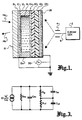
- FIG. 1 a modified form of an LCLV is shown which provides a high resolution display of an electron beam scan pattern.
- a CRT is represented as an electron beam generator 2 and a pair of deflection plates 4 which cause the beam 6 to scan in a raster pattern. An additional pair of plates would also be provided to control the beam scan into and out of the page.
- the beam current is typically in the approximate range of 10 microamps to 1 milliamp.
- the LCLV includes a layer of liquid crystal 8 which is enclosed in a cell formed by insulating films 10 and 10a on either side to provide electrical and chemical isolation, and spacers 12 and 12a which maintain a suitable gap between insulating films 10 and 10a and prevent liquid crystal 8 from escaping.
- the left side of the LCLV is referred to as the "readout" side, since an optical readout beam 14a is directed onto the valve from this side and is reflected as an output beam 14b after it has been modulated in accordance with the electron beam pattern.
- a transparent cover plate 16 preferably made from glass, covers and protects the left hand side of the device.
- a transparent electrode 18, preferably formed from indium tin oxide, is located on the inner face of cover plate 16. This electrode provides a reference for the voltage established across the liquid crystal, as described below.
- a mirror 20 is provided on the opposite side of the liquid crystal cell from the readout beam. This mirror receives the readout beam and reflects it back again through the liquid crystal. It can be implemented with a conventional wide band, high reflectivity dielectric mirror. This is in contrast to many light valves, which employ a photoconductive layer; this construction requires the mirror to have a limited bandwidth, since the mirror is required to absorb almost all of the readout light which is not reflected so as to avoid rendering the photoconductive layer conductive.
- the present light valve does not employ a photoconductive layer, and therefore the mirror can be wide band.
- a metal matrix mirror such as that disclosed in pending U.S. patent application Serial No. 759,004, "Reflective Matrix Mirror Visible to Infrared Convertor Light Valve" by P. O. Braatz and assigned to Hughes Aircraft Company, the assignee of the present invention, may also be employed.
- a support membrane 22 is positioned on the electron beam side of mirror 20, and supports both the mirror and a layer of partially conductive material 24.
- the membrane should be resistive so as to avoid shorting the partially conductive layer, with a high sheet resistivity in the order of 1012 ohms/sq. or greater. It is either rigid, or stretchable so that it can be formed with a very flat surface plane; an outer ring (not shown) may be provided as a base for stretching the membrane.
- the membrane should be clear so as to not absorb light, which can cause it to heat up and become physically distorted or transfer heat to the liquid crystal. Suitable membrane materials are Kapton, mica, Al2O3 and boron nitride. To protect it from possible electron damage, the membrane might incorporate a thin layer of SiO2 or other resistive material evaporated onto its electron beam side.
- a thin sheet of a conductive material 26 is formed on the electron beam face of the partially conductive layer, and preferably extends continuously across that layer.
- the conductive sheet is preferably deposited as a film by an evaporation process. It is kept quite thin, generally on the order of about 200-1,000 angstroms, so as to not present a substantial barrier to the electron beam. Most of the beam penetrates the conductive sheet and enters the partially conductive layer.
- Either a metal or a highly doped semiconductor can be used for the conductive sheet, but semiconductors do not have sufficient broadband reflectivity to also function as a mirror.
- Aluminum is preferred because it is easy to work with, fairly inert and a good broadband reflector.
- Other suitable metals include silver, chrome and nickel.
- the conductive sheet 26 and the electrode 18 are connected together to ground or, in an alternate embodiment, an AC voltage source 30 may be connected between these elements as described below.
- the dimensions of the conductive sheet and the underlying partially conductive layer, and the conductivity of the partially conductive layer, are selected so that electrons absorbed within each pixel of the partially conductive layer during a particular scan will leak out to the conductive sheet by the time the electron beam has finished a scanning cycle and returned to that pixel. For a television scan rate of 30-60 Hz, the leakage rate should be fast enough to dissipate the pixel in the approximately 17-30 milliseconds between scans.
- the dissipation through the partially conductive layer should be slow enough to permit the readout beam 14a to read the image before the image dissipates.
- the bulk resistivity of the partially conductive layer is preferably within the range of about 109-1011 ohm cm, and its thickness is preferably about 2-10 microns ( ⁇ m).
- Suitable partially conductive materials include silicon dioxide, amorphous silicon and cryolite; cadmium telluride may be acceptable in some applications, but for others it may be too conductive.
- doped SiO2 with a dielectric constant of about 4.5x10 ⁇ 13, a resistivity of about 2x10¹⁰ ohm cm will produce a charge dissipation time constant of about 10 millisec for a 30 millisec frame rate.
- the partially conductive material can have a resistivity considerably greater than that used for the corresponding material in the related co-pending application Serial No. 927,580. This is because the electrons in the beam which penetrate into the partially conductive material in general have a much longer distance to flow back out to the conductive grid in the related application. Whereas the electrons are generally implanted only about 1-2 microns into the partially conductive layer, the grid openings may be on the order of about 100 microns on each side.
- the electrons have to flow back only about 1-2 microns to reach the sheet, whereas electrons which hit the partially conductive material in the middle of a grid opening have to flow about 50 microns laterally in addition to the 1-2 microns backward to reach the grid.
- An adverse result of this phenomenon for the present invention is that the effect of the implanted electrons upon the liquid crystal is reduced for the same implant energy. This is because, if each layer of material is assumed to have parallel sides and a uniform dielectric constant, the effect on the liquid crystal of a particular electron implant will vary with the depth of implant beyond the back electrode 26, relative to the effective distance between the back and front electrodes 26 and 18. Since the average distance between the implanted electrons and the back electrode with a conductive grid is much greater than the average electron implant depth relative to a conductive sheet, the effect of the electron implant upon the liquid crystal will be correspondingly reduced when the back electrode is a conductive sheet 26. To compensate for this, either a higher electron implant voltage or current density is required with the present invention to compensate for the lower effective implant depth. In practice it is normally easier to increase both voltage and current density somewhat, rather than increasing only one or the other.
- the electron charge absorbed into any particular pixel of the partially conductive layer 24 as a result of the electron beam scan produces a voltage across a corresponding location of the liquid crystal. Since the various elements of the light valve have a high resistance to lateral spreading, an essentially 1:1 correspondence can be achieved between the individual pixel areas of the partially conductive layer which receive electron charges, and corresponding areas of the liquid crystal which support a voltage determined by the absorbed charge. To avoid an excessive voltage drop across the membrane at the expense of the liquid crystal voltage, the membrane should be made quite thin, in the order of about 4-12 microns.
- the pixel voltages established across the liquid crystal from an electron beam scan can be made AC rather than DC.
- An AC operation is a distinct advantage, since liquid crystal tends to decompose under sustained DC operation.
- the liquid crystal polarization shift responds to the RMS voltage level, so that an AC voltage may be used to establish the polarization shift without the decomposition effects of DC operation.
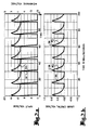
- the calculated input voltage 32 resulting from the electron beam scanning a particular pixel location, and the voltage 34 across the membrane, are shown in FIG. 2a, while the steady state voltage 36 across the liquid crystal after an initial transient period is shown in FIG. 2b.
- the beam scans the liquid crystal in a very short period of time, rapidly depositing electrons which produce voltage peaks 38 across the liquid crystal.
- the electron beam will typically deposit charge onto a pixel over a time period in the order of about 30 nsec. After the beam has passed, the electrons absorbed into the pixel will begin to flow back out to the right towards the conductive sheet 26, from whence they are dissipated to ground.
- AC power supply 30 can be used to bias the liquid crystal to a voltage near its threshold voltage, so as to improve its sensitivity. After the electron beam has passed a given pixel and a maximum voltage has been produced across the liquid crystal, the liquid crystal voltage gradually decays along line 40 back to its original value.
- the area under the negative portion of the liquid crystal voltage curve will generally be equal to the area under the positive portion of the curve, resulting in an AC liquid crystal voltage characteristic over the course of repeated beam scans. This avoids the deterioration problem associated with DC operation, discussed above. On the other hand, the voltage decay is slow enough so that the liquid crystal has enough time to respond and produce the desired image.
- the decay of the liquid crystal voltage field is controlled by the membrane time constant R M C M , where R M and C M are respectively the resistance and capacitance of the membrane.
- R M and C M are respectively the resistance and capacitance of the membrane.
- E represents the voltage resulting from the charge deposited in a particular pixel by the electron beam
- R PC and C PC are respectively the resistance and capacitance of the partially conductive layer
- R LC and C LC are respectively the resistance and capacitance of the liquid crystal
- I B is the beam current and t is time, for one pixel element.
- the membrane and partially conductive layer capacitances are generally of the same order of magnitude, whereas the membrane sheet resistivity is generally much greater than that of the partially conductive layer.
- the charge deposited by the electron beam can flow out to the conductive sheet 26 either directly through the partially conductive layer, or through a parallel path consisting of the bulk of the membrane and liquid crystal to electrode 18.
- the device has a very fast response time, being limited principally only by the liquid crystal. It also has a very simple structure that eliminates the need for fiber optics coupling plates or input imaging lenses used with prior devices. An image is produced with a high degree of uniformity, since each pixel of the partially conductive layer discharges directly into the adjacent conductive grid. It is also considerably more sensitive than the prior Tektronix or similar devices - since the present light valve is reflective rather than transmissive, the readout beam passes through the liquid crystal twice, both before and after reflection. This will permit a thinner liquid crystal layer to be used for the same sensitivity, or conversely will produce a greater sensitivity for the same liquid crystal thickness. Since the liquid crystal response time varies with the square of its thickness, any reduction in thickness will have a very positive effect upon responsivity.
- the mirror 20 is deposited onto the membrane 22 in one deposition run, and the partially conductive layer 24 is deposited onto the membrane in a separate deposition run. It would also be possible to reverse the positions of the membrane and mirror, so that the mirror is sandwiched between the membrane and partially conductive layer on the electron beam side of the membrane. This could enable the fabrication of these elements to be accomplished in a single deposition run.
- the membrane however, would have to be transparent to permit passage of the readout light beam to the mirror.
- FIG. 4 shows the light valve integrated within a CRT.
- the light valve is similar to that shown in FIG. 1, and the same reference numerals are used for common elements.
- the conductive sheet 26 itself serves as the mirror.
- the membrane 22 should be generally transparent and non-birefringent in this application, as should the partially conductive layer 24.
- a readout beam is applied to the light valve from the right and penetrates all the way to the conductive sheet 26, where it is reflected back through the liquid crystal layer and out of the valve. Numerous other variations and alternate embodiments will also occur to those skilled in the art. Accordingly, it is intended that the invention be limited only in terms of the appended claims.
Landscapes
- Physics & Mathematics (AREA)
- Nonlinear Science (AREA)
- Mathematical Physics (AREA)
- Chemical & Material Sciences (AREA)
- Crystallography & Structural Chemistry (AREA)
- General Physics & Mathematics (AREA)
- Optics & Photonics (AREA)
- Liquid Crystal (AREA)
Abstract
Claims (17)
- Modulateur de lumière à cristaux liquides (MLCL) adressable sur une face par un faisceau d'électrons de balayage (6) et, sur une autre face, par un faisceau optique de lecture (14a, b), comprenant :
une couche de cristaux liquides (8) adressable par le faisceau optique de lecture (14a,b), et
une membrane électriquement résistive (22) fixée sur un support à proximité de la couche de cristaux liquides (8) du côté de cette couche destiné à recevoir le faisceau d'électrons,
caractérisé par
la présence d'une couche d'une matière partiellement conductrice (24) supportée par la membrane (22) et adressable par le faisceau d'électrons (6), l'accumulation d'une charge électrique dans la couche partiellement conductrice (24) par le balayage par le faisceau d'electrons (6) produisant une tension à travers le cristal liquide (8),
la présence d'une feuille conductrice (26) perméable à un faisceau d'électrons disposée du côté destiné à recevoir le faisceau d'électrons de la couche partiellement conductrice (24), ladite feuille (26) étant apte à transmettre au moins partiellement un faisceau d'électrons appliqué (6) à la couche partiellement conductrice (24) et à recueillir la charge reçue par la couche partiellement conductrice (24) en résultat du balayage par le faisceau d'électrons (6) de cette couche, et la présence d'un circuit pour dissiper la charge reçue par la couche conductrice (26) à partir de la couche partiellement conductrice (24). - MLCL suivant la revendication 1, dans lequel les dimensions et les matières des divers éléments sont choisies par rapport à la vitesse de balayage par le faisceau d'électrons (6), de manière à produire un débit d'électrons à partir de la couche partiellement conductrice (24) dans la feuille conductrice (26) qui est suffisamment rapide pour dissiper fortement les électrons délivrés à la couche partiellement conductrice (24) au cours d'un balayage par le faisceau d'électrons (6) avant le balayage suivant, mais suffisamment lent pour que le cristal liquide (8) produise une image pour le faisceau de lecture (14a,b).
- MLCL suivant la revendication 1 ou 2, dans lequel la résistance d'au moins l'une des couches du MLCL est suffisamment grande pour produire une forte tension CA à travers le cristal liquide (8) après chaque balayage par le faisceau d'électrons (6).
- MLCL suivant au moins l'une des revendications 1 à 3, dans lequel une électrode transparente (18) est placée sur le côté destiné au faisceau de lecture de la couche de cristal liquide (8) pour fournir une tension de référence à la couche de cristal liquide (8).
- MLCL suivant la revendication 4, dans lequel le circuit comprend une connexion mutuelle entre la feuille conductrice (26) et l'électrode transparente (18).
- MLCL suivant la revendication 5, dans lequel la feuille conductrice (26) et l'électrode transparente (18) sont mises à la terre.
- MLCL suivant la revendication 5 ou 6, dans lequel le circuit comprend une source de courant alternatif (30) connectée entre la feuille conductrice (26) et l'électrode transparente (18).
- MLCL suivant au moins l'une des revendications 1 à 7, comprenant en outre un miroir (20) disposé du côté destiné à recevoir le faisceau d'électrons de la couche de cristaux liquides (8) et apte à réfléchir un faisceau de lecture (14a,b) reçu par la couche de cristaux liquides (8) en le renvoyant à travers cette couche.
- MLCL suivant la revendication 8, dans lequel le miroir (20) est positionné entre la couche de cristaux liquides (8) et la membrane (22).
- MLCL suivant au moins l'une des revendications 1 à 7, dans lequel la couche partiellement conductrice (24) et la membrane (22) sont généralement transparentes et non biréfringentes, et la feuille conductrice (26) est réfléchissante du côté du faisceau de lecture pour réfléchir un faisceau de lecture reçu (14a,b) en le renvoyant à travers la couche de cristaux liquides (8).
- MLCL suivant au moins l'une des revendications 1 à 10, dans lequel la feuille conductrice (26) est pratiquement continue à travers la couche partiellement conductrice (24).
- MLCL suivant au moins l'une des revendications 1 à 11, dans lequel la feuille conductrice (26) comprend un métal.
- MLCL suivant la revendication 12, dans lequel la feuille conductrice (26) est formée à partir d'un métal du groupe comprenant l'aluminium, l'argent, le chrome et le nickel.
- MLCL suivant au moins l'une des revendications 1 à 13, dans lequel la feuille conductrice (26) possède une épaisseur comprise dans l'intervalle d'environ 200 à environ 1000 angströms.
- MLCL suivant la revendication 14, dans lequel la feuille conductrice (26) comprend un film mince formé par évaporation sur la couche partiellement conductrice (24).
- MLCL suivant au moins l'une des revendications 1 à 15, dans lequel la couche partiellement conductrice (24) possède une résistance apparente de l'ordre d'environ 10⁹ à 10¹¹ ohms/cm.
- MLCL suivant au moins l'une des revendications 1 à 16, dans lequel l'épaisseur de la membrane (22) est comprise dans l'intervalle approximatif de 4 à 12 µm, l'épaisseur de la couche partiellement conductrice (24) est comprise dans l'intervalle approximatif de 2 à 6 µm, et l'épaisseur de la couche de cristaux liquides (8) est comprise dans l'intervalle approximatif de 1 à 25 µm.
Applications Claiming Priority (2)
| Application Number | Priority Date | Filing Date | Title |
|---|---|---|---|
| US07/021,381 US4826293A (en) | 1987-03-03 | 1987-03-03 | Electron beam addressed liquid crystal light valve with input sheet conductor |
| US21381 | 1993-02-23 |
Publications (2)
| Publication Number | Publication Date |
|---|---|
| EP0303686A1 EP0303686A1 (fr) | 1989-02-22 |
| EP0303686B1 true EP0303686B1 (fr) | 1993-04-07 |
Family
ID=21803867
Family Applications (1)
| Application Number | Title | Priority Date | Filing Date |
|---|---|---|---|
| EP88902992A Expired - Lifetime EP0303686B1 (fr) | 1987-03-03 | 1988-01-25 | Relais variateur de lumiere de cristaux liquides adresse par un faisceau d'electrons avec conducteur a feuille d'entree |
Country Status (6)
| Country | Link |
|---|---|
| US (1) | US4826293A (fr) |
| EP (1) | EP0303686B1 (fr) |
| JP (1) | JPH01502856A (fr) |
| CA (1) | CA1298646C (fr) |
| DE (1) | DE3880046T2 (fr) |
| WO (1) | WO1988006746A1 (fr) |
Families Citing this family (19)
| Publication number | Priority date | Publication date | Assignee | Title |
|---|---|---|---|---|
| US7864151B1 (en) | 1986-07-07 | 2011-01-04 | Semiconductor Energy Laboratory Co., Ltd. | Portable electronic device |
| DE68919249T2 (de) * | 1988-03-23 | 1995-03-23 | Seiko Instr Inc | Optisch geschaltete ferroelektrische Flüssigkeitskristallichtabsperrvorrichtung. |
| JPH0229623A (ja) * | 1988-07-19 | 1990-01-31 | Semiconductor Energy Lab Co Ltd | 液晶表示装置 |
| US4941735A (en) * | 1989-03-02 | 1990-07-17 | University Of Colorado Foundation, Inc. | Optically addressable spatial light modulator |
| US5076670A (en) * | 1989-10-13 | 1991-12-31 | Hughes Aircraft Company | Isolated pixel liquid crystal light valve structure |
| WO1992016872A1 (fr) * | 1991-03-20 | 1992-10-01 | Mitsubishi Denki Kabushiki Kaisha | Dispositif d'affichage du type a projection |
| US5379136A (en) * | 1993-10-04 | 1995-01-03 | Hu; Shouxiang | Electron beam addressed electro-optical light valve having input openings |
| US6236445B1 (en) | 1996-02-22 | 2001-05-22 | Hughes Electronics Corporation | Method for making topographic projections |
| US5768009A (en) * | 1997-04-18 | 1998-06-16 | E-Beam | Light valve target comprising electrostatically-repelled micro-mirrors |
| US6034810A (en) * | 1997-04-18 | 2000-03-07 | Memsolutions, Inc. | Field emission charge controlled mirror (FEA-CCM) |
| US6005692A (en) * | 1997-05-29 | 1999-12-21 | Stahl; Thomas D. | Light-emitting diode constructions |
| US6028696A (en) * | 1998-10-15 | 2000-02-22 | Memsolutions, Inc. | Charge controlled mirror with improved frame time utilization and method of addressing the same |
| US6038058A (en) * | 1998-10-15 | 2000-03-14 | Memsolutions, Inc. | Grid-actuated charge controlled mirror and method of addressing the same |
| US5991066A (en) * | 1998-10-15 | 1999-11-23 | Memsolutions, Inc. | Membrane-actuated charge controlled mirror |
| US6031657A (en) * | 1998-10-15 | 2000-02-29 | Memsolutions, Inc. | Membrane-actuated charge controlled mirror (CCM) projection display |
| US6123985A (en) * | 1998-10-28 | 2000-09-26 | Solus Micro Technologies, Inc. | Method of fabricating a membrane-actuated charge controlled mirror (CCM) |
| US6995821B1 (en) * | 1999-04-23 | 2006-02-07 | International Business Machines Corporation | Methods of reducing unbalanced DC voltage between two electrodes of reflective liquid crystal display by thin film passivation |
| US6346776B1 (en) | 2000-07-10 | 2002-02-12 | Memsolutions, Inc. | Field emission array (FEA) addressed deformable light valve modulator |
| US20030160105A1 (en) * | 2002-02-22 | 2003-08-28 | Kelly Arnold J. | Methods and apparatus for dispersing a conductive fluent material |
Citations (1)
| Publication number | Priority date | Publication date | Assignee | Title |
|---|---|---|---|---|
| WO1988003664A1 (fr) * | 1986-11-06 | 1988-05-19 | Hughes Aircraft Company | Variateur de lumiere a cristaux liquides adresse par un faisceau electronique |
Family Cites Families (5)
| Publication number | Priority date | Publication date | Assignee | Title |
|---|---|---|---|---|
| US3650608A (en) * | 1969-12-23 | 1972-03-21 | Texas Instruments Inc | Method and apparatus for displaying coherent light images |
| FR2163856A5 (fr) * | 1971-12-03 | 1973-07-27 | Thomson Csf | |
| CA1041643A (fr) * | 1974-05-10 | 1978-10-31 | Xerox Corporation | Systeme de formation d'images |
| US4387964A (en) * | 1980-10-21 | 1983-06-14 | Mcdonnell Douglas Corporation | Electron addressed liquid crystal light valve |
| DE3229083A1 (de) * | 1982-08-04 | 1984-02-09 | Andreas 2950 Leer Otten | Vakuumroehre zum einlesen von bildern in fluessigkristallzellen |
-
1987
- 1987-03-03 US US07/021,381 patent/US4826293A/en not_active Expired - Lifetime
-
1988
- 1988-01-25 JP JP63502715A patent/JPH01502856A/ja active Pending
- 1988-01-25 WO PCT/US1988/000181 patent/WO1988006746A1/fr not_active Ceased
- 1988-01-25 EP EP88902992A patent/EP0303686B1/fr not_active Expired - Lifetime
- 1988-01-25 DE DE8888902992T patent/DE3880046T2/de not_active Expired - Fee Related
- 1988-02-10 CA CA000558646A patent/CA1298646C/fr not_active Expired - Fee Related
Patent Citations (1)
| Publication number | Priority date | Publication date | Assignee | Title |
|---|---|---|---|---|
| WO1988003664A1 (fr) * | 1986-11-06 | 1988-05-19 | Hughes Aircraft Company | Variateur de lumiere a cristaux liquides adresse par un faisceau electronique |
Also Published As
| Publication number | Publication date |
|---|---|
| WO1988006746A1 (fr) | 1988-09-07 |
| JPH01502856A (ja) | 1989-09-28 |
| DE3880046T2 (de) | 1993-07-15 |
| EP0303686A1 (fr) | 1989-02-22 |
| CA1298646C (fr) | 1992-04-07 |
| DE3880046D1 (de) | 1993-05-13 |
| US4826293A (en) | 1989-05-02 |
Similar Documents
| Publication | Publication Date | Title |
|---|---|---|
| EP0289544B1 (fr) | Variateur de lumiere a cristaux liquides adresse par un faisceau electronique | |
| EP0303686B1 (fr) | Relais variateur de lumiere de cristaux liquides adresse par un faisceau d'electrons avec conducteur a feuille d'entree | |
| US4925276A (en) | Liquid crystal light valve utilizing hydrogenated amorphous silicon photodiode | |
| US5084777A (en) | Light addressed liquid crystal light valve incorporating electrically insulating light blocking material of a-SiGe:H | |
| US4538884A (en) | Electro-optical device and method of operating same | |
| US3840695A (en) | Liquid crystal image display panel with integrated addressing circuitry | |
| US5177628A (en) | Self-powered optically addressed spatial light modulator | |
| US4158201A (en) | Flat electro optic display panel and method of using same | |
| US4191454A (en) | Continuous silicon MOS AC light valve substrate | |
| US4443064A (en) | High resolution AC silicon MOS-light-valve substrate | |
| US4198647A (en) | High resolution continuously distributed silicon photodiode substrate | |
| EP0707304B1 (fr) | Procédé de commande pour un modulateur spatial de lumière et système d'affichage par projection | |
| US5220445A (en) | Optical image processor | |
| EP0348499B1 (fr) | Systeme et procede de production d'une image video sans scintillement | |
| US5210628A (en) | Liquid crystal light valve with photosensitive layer having irregular diode pattern | |
| US4010321A (en) | Light modulating device using schlieren lens system | |
| EP0189028A2 (fr) | Transducteur d'images optique-optique capable d'accepter les radiations à rayons X | |
| USH840H (en) | Single-Schottky diode liquid crystal light valve and method | |
| GB1604206A (en) | Ac driven liquid crystal light valve | |
| US5612800A (en) | LCLV having photoconductive pedestals each having a cross-sectional area no greater than 5 percent of the area of its respective reflective pad | |
| EP0331724A1 (fr) | Relais optique a cristaux liquides a diode schottky unique et procede de production | |
| JPS62242919A (ja) | 光導電型液晶ライトバルブ | |
| EP0326467B1 (fr) | Obturateur sélectif de lumière, procédé de réalisation, et son application à un détecteur d'image | |
| JP3070252B2 (ja) | 空間光変調素子および表示装置 | |
| US3708712A (en) | Intelligence-handling device having means for limiting induced electrostatic potential |
Legal Events
| Date | Code | Title | Description |
|---|---|---|---|
| PUAI | Public reference made under article 153(3) epc to a published international application that has entered the european phase |
Free format text: ORIGINAL CODE: 0009012 |
|
| 17P | Request for examination filed |
Effective date: 19881102 |
|
| AK | Designated contracting states |
Kind code of ref document: A1 Designated state(s): CH DE FR GB LI NL |
|
| 17Q | First examination report despatched |
Effective date: 19910429 |
|
| GRAA | (expected) grant |
Free format text: ORIGINAL CODE: 0009210 |
|
| AK | Designated contracting states |
Kind code of ref document: B1 Designated state(s): CH DE FR GB LI NL |
|
| REF | Corresponds to: |
Ref document number: 3880046 Country of ref document: DE Date of ref document: 19930513 |
|
| ET | Fr: translation filed | ||
| PGFP | Annual fee paid to national office [announced via postgrant information from national office to epo] |
Ref country code: FR Payment date: 19931208 Year of fee payment: 7 |
|
| PGFP | Annual fee paid to national office [announced via postgrant information from national office to epo] |
Ref country code: GB Payment date: 19931210 Year of fee payment: 7 |
|
| PGFP | Annual fee paid to national office [announced via postgrant information from national office to epo] |
Ref country code: DE Payment date: 19931217 Year of fee payment: 7 Ref country code: CH Payment date: 19931217 Year of fee payment: 7 |
|
| PGFP | Annual fee paid to national office [announced via postgrant information from national office to epo] |
Ref country code: NL Payment date: 19940131 Year of fee payment: 7 |
|
| PLBE | No opposition filed within time limit |
Free format text: ORIGINAL CODE: 0009261 |
|
| STAA | Information on the status of an ep patent application or granted ep patent |
Free format text: STATUS: NO OPPOSITION FILED WITHIN TIME LIMIT |
|
| 26N | No opposition filed | ||
| PG25 | Lapsed in a contracting state [announced via postgrant information from national office to epo] |
Ref country code: GB Effective date: 19950125 |
|
| PG25 | Lapsed in a contracting state [announced via postgrant information from national office to epo] |
Ref country code: LI Effective date: 19950131 Ref country code: CH Effective date: 19950131 |
|
| PG25 | Lapsed in a contracting state [announced via postgrant information from national office to epo] |
Ref country code: NL Effective date: 19950801 |
|
| GBPC | Gb: european patent ceased through non-payment of renewal fee |
Effective date: 19950125 |
|
| PG25 | Lapsed in a contracting state [announced via postgrant information from national office to epo] |
Ref country code: FR Effective date: 19950929 |
|
| REG | Reference to a national code |
Ref country code: CH Ref legal event code: PL |
|
| NLV4 | Nl: lapsed or anulled due to non-payment of the annual fee |
Effective date: 19950801 |
|
| PG25 | Lapsed in a contracting state [announced via postgrant information from national office to epo] |
Ref country code: DE Effective date: 19951003 |
|
| REG | Reference to a national code |
Ref country code: FR Ref legal event code: ST |