EP0303712A1 - Anordnung zum nachweis der ausgangsspannung eines laser-oszillators - Google Patents
Anordnung zum nachweis der ausgangsspannung eines laser-oszillators Download PDFInfo
- Publication number
- EP0303712A1 EP0303712A1 EP88901930A EP88901930A EP0303712A1 EP 0303712 A1 EP0303712 A1 EP 0303712A1 EP 88901930 A EP88901930 A EP 88901930A EP 88901930 A EP88901930 A EP 88901930A EP 0303712 A1 EP0303712 A1 EP 0303712A1
- Authority
- EP
- European Patent Office
- Prior art keywords
- output voltage
- voltage
- laser oscillator
- laser
- current
- Prior art date
- Legal status (The legal status is an assumption and is not a legal conclusion. Google has not performed a legal analysis and makes no representation as to the accuracy of the status listed.)
- Granted
Links
Images


Classifications
-
- G—PHYSICS
- G01—MEASURING; TESTING
- G01R—MEASURING ELECTRIC VARIABLES; MEASURING MAGNETIC VARIABLES
- G01R19/00—Arrangements for measuring currents or voltages or for indicating presence or sign thereof
- G01R19/145—Indicating the presence of current or voltage
- G01R19/155—Indicating the presence of voltage
-
- G—PHYSICS
- G01—MEASURING; TESTING
- G01R—MEASURING ELECTRIC VARIABLES; MEASURING MAGNETIC VARIABLES
- G01R19/00—Arrangements for measuring currents or voltages or for indicating presence or sign thereof
-
- H—ELECTRICITY
- H01—ELECTRIC ELEMENTS
- H01S—DEVICES USING THE PROCESS OF LIGHT AMPLIFICATION BY STIMULATED EMISSION OF RADIATION [LASER] TO AMPLIFY OR GENERATE LIGHT; DEVICES USING STIMULATED EMISSION OF ELECTROMAGNETIC RADIATION IN WAVE RANGES OTHER THAN OPTICAL
- H01S3/00—Lasers, i.e. devices using stimulated emission of electromagnetic radiation in the infrared, visible or ultraviolet wave range
- H01S3/0014—Monitoring arrangements not otherwise provided for
-
- H—ELECTRICITY
- H01—ELECTRIC ELEMENTS
- H01S—DEVICES USING THE PROCESS OF LIGHT AMPLIFICATION BY STIMULATED EMISSION OF RADIATION [LASER] TO AMPLIFY OR GENERATE LIGHT; DEVICES USING STIMULATED EMISSION OF ELECTROMAGNETIC RADIATION IN WAVE RANGES OTHER THAN OPTICAL
- H01S3/00—Lasers, i.e. devices using stimulated emission of electromagnetic radiation in the infrared, visible or ultraviolet wave range
- H01S3/09—Processes or apparatus for excitation, e.g. pumping
- H01S3/097—Processes or apparatus for excitation, e.g. pumping by gas discharge of a gas laser
- H01S3/0975—Processes or apparatus for excitation, e.g. pumping by gas discharge of a gas laser using inductive or capacitive excitation
Definitions
- the present invention relates to an output voltage detecting device in a laser oscillator, and more particularly to an output voltage detecting device in a laser oscillator, in which an output voltage can be detected with a circuit of a simple configuration.
- a laser tube for use in a gas laser device has an electrical impedance which varies depending upon an interiorly confined gas status, as a consequence, a voltage supplied to the laser tube varies.
- the variation in the electrical impedance of the laser tube causes to vary the supply voltage, since the current is being controlled to be at constant. If this condition is left as it stands, semiconductor elements, the laser tube or other elements constituting an inverter are caused to be damaged.
- a method in which the voltage is divided by capacitors is involved with a problem such that a power supply line led to the laser tube cannot be isolated from a ground connection of a control apparatus, so that noises are liable to be introduced into a control circuit.
- An object of the invention is to resolve the foregoing problems and to provide an output voltage detecting device in a laser oscillator, in which an output voltage is detected with a circuit of a simple configuration, and an abnormal voltage can be monitored.
- Another object of the invention is to provide an output voltage detecting device in a laser oscillator, which is operable at a low voltage and producible at an inexpensive cost.
- the present invention provides an output voltage detecting device in a laser oscillator in which a laser oscillation is taken place upon application of a high frequency voltage to a laser tube.
- the device comprises a voltage detection circuit connected to an input of an inverter for applying the high frequency voltage, the voltage detecting circuit including a nonlinear element and a referernce voltage, a current transformer for detecting a current flowing in the nonlinear element, and wherein abnormality of the output voltage is detected in accordance with the current flowing in the nonlinear element (B).
- the nonlinear element has a nonlinear point at a voltage slightly higher than a regular voltage of a converter, and a current vs. resistance relation is abruptly changed when the voltage applied thereto exceeds the nonlinear point voltage. Accordingly, when the output voltage of the converter exceeds the reference voltage, a current flows abruptly in the nonlinear element. Thus, upon detection of the current by means of the current transformer, an abnormal voltage is detected.
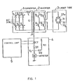
- FIG. 1 is a block diagram showing a first embodiment of the invention, in which a converter 1 converts a current from a commercial power supply to a D.C. current upon rectification.
- the converter is comprised of six SCRs Sl through S6.
- An inverter 2 modulates the D.C. output voltage from the converter 1 to a high frequency voltage at several megahertz, which is in the form of a bridge circuit composed of four FETs.
- a laser tube 3 includes a tube 31 formed, for example, with a silica glass, in the interior of which a laser medium gas 32 is circulated, and electrodes 33a and 33b which apply the high frequency voltage to the tube 31.
- a discharge is taken place by applying the high frequency voltage to the laser medium gas 32 confined within the tube 31, whereby the laser light is oscillated and amplified.
- the direction in which the laser light emits is perpendicular to the surface of the sheet of the drawing.
- a current detection circuit 4 is connected to the output of the converter 1.
- the line extending from the converter 1 is coupled to a current transformer CT and is then connected to a diode D1.
- the diode D1 is connected to a varistor B which is a nonlinear element. Opposite terminal of the varistor B is connected to ground.
- the varistor is further connected to a diode D2, and the anode of the diode D2 is connected through a resistor R1 to a reference voltage V.
- the reference voltage V is set to 5 to 10 % higher than a normal voltage of the converter 1.
- the varistor B as used has a nonlinear point, i.e. a point in which a resistance characteristic varies, higher by 10 volts or so than the reference voltage. Accordingly, the voltage VS depicted in the figure is lower than the nonlinear point of the varistor B when the output voltage of the converter 1 is normal, in which case a current little flows in the diode Dl.
- a control unit 5 detects an abnormal voltage responsive to a rising edge of the current flowing in the current transformer CT, whereupon an alarm is generated.
- the gate signals of the thyristors in the converter 1 are rendered off to thereby stop driving.
- FIG. 2 there is depicted a relation between the output voltage and the current of the converter 1.
- the ordinate represents the voltage VS in FIG. 1 and the abscissa represents time.
- the current I is abruptly flowed in the varisster B.
- the current flowing therein can be detected by the current transformer CT.
- the abnormal voltage can thus be detected with a circuit of a simple configuration and the semiconductor elements including FETs in the inverter 2 can be protected. Further, since the ground-connected terminals of the converter 1 and the inverter 2 are not connected to the current transformer CT, there is little possibility that the noises are introduced into the control unit 5.
- the varistor has been exemplified as a nonlinear element, other kinds of non-linear elements, such as a Zenor diode operabhle at a high voltage, can also be employed.
- the nonlinear element for detecting the abnormal voltage
- the variation in the current level is detected. Therefore, the abnormal voltage can be detected with a circuit of a simple configuration. In addition, it is capable of reducing the possibility that the noises are introduced into the circuits of the control unit.
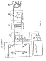
- FIG. 3 is a block diagram showing a second embodiment of the invention.
- a high frequency power supply unit 11 supplies a high frequency voltage upon rectifying a current from a commercial power supply to provide a D.C. current and then converting it to the high frequency voltage using a high frequency inverter.
- a booster transformer 12 boosts the high frequency voltage supplied from the high frequency power supply unit 11 to a required voltage.
- a matching circuit 13 performs an impedance matching between the transformer 12 and a laser tube, so that power fed from the high frequency power supply unit 11 is effectively supplied to the laser tube.
- a ⁇ -type matching circuit is employed.
- Capacitors C31 and C33 are parallel-connected reactances and an inductor L32 is a serially-connected reactance.
- the laser tube 14 has a tube 141 formed with, for example, a silica glass.
- a laser medium gas 142 is being circulated.
- electrodes 143a and 143b Through electrodes 143a and 143b, a high frequency voltage is applied to the tube 141.
- a discharge is taken place for the laser medium gas 142 confined within the laser tube 141 while applying a high frequency voltage, whereupon the laser light is oscillated and amplified.
- the direction in which the laser light emits is perpendicular to the sheet of the drawing.
- a current transformer 15 is coupled to the ground-connected terminal of a primary winding of the transformer 12. Accordingly, the voltage induced in the current transformer 15 is extremely low, and thus the current transformers of low insulation voltage are available. Since a ground terminal of the current transformer 15 is isolated from a power line for the laser discharge, there is little possibility that noises are introduced into the current transformer.
- An amplifier 17 is provided in which assuming that its amplification factor K is an impedance of the primary winding impedance of the transformer, the output of the amplifier is defined by a product of a current fed from the current transformer 15 and an impedance of the primary winding of the transformer. A voltage of the high frequency power supply unit is thereby calculated.
- the voltage supplied to the laser tube can be calculated in a control circuit 16 in such a manner that the current fed from the current transformer 15 is converted to a digital value with the use of a DA converter and a product of the resultant value and the impedance of the primary winding of the transformer is obtained, where the impedance of the primary winding of the transformer has been stored in advance in the form of a digital value.
- the FETs used in the high frequency power supply unit 11 can be protected owing to the detection voltage.
- the voltage thus obtained is compared with a predetermined reference voltage, and when it is above the reference voltage by a predetermined value, an alarm is generated.
- the driving is stopped. Furthermore, while monitoring the voltage obtained, it may automatically be controlled so as to be at constant.
- the current transformer is coupled to the primary winding of the transformer, it is possible to modify the transformer 12 to have three windings while dispensing with a special current transformer.
- the output voltage of the high frequency power supply unit is detected on the basis of the current detected by the current transformer provided in the ground terminal of the primary winding of the transformer, current transformers having low insulation volltages and inexpensive in cost are available, and the output voltage of the high frequency power supply unit can be measured with a circuit of a simple configuration.
- FIG. 4 is a block diagram showing the embodiment of the invention.
- an inverter 21 rectifies a current from a commercial power supply to provide a D.C. current and then converts it to the high frequency voltage.
- a tank circuit 22 is connected in parallel to the output of the inverter 21, and is made up of a coil L and a capacitor C connected in parallel to each other.
- the tank circuit has a high sharpness of resonance Q, in which the coil L and the capacitor C are selected so that the impedance of the tank circuit 22 as viewed from the side of the inverter 21 is substantially purely resistive.
- a booster transformer 23 boosts the high frequency voltage supplied from the inverter 21 to a required voltage.
- a matching circuit 24 performs an impedance matching between the transformer 23 and a laser tube 26, so that power fed from the inverter 21 is effectively supplied to the laser tube.
- a ⁇ -type matching circuit is employed.
- Capacitors C1 and C2 are parallel-connected reactances and an inductor L1 is a serially-connected reactance.
- the laser tube 25 has a tube 251 formed with, for example, a silica glass.
- a laser medium gas 252 is being circulated.
- electrodes 253a and 253b Through electrodes 253a and 253b, a high frequency voltage is applied to the tube 251.
- a discharge is taken place for the laser medium gas 242 confined within the laser tube 251 while applying a high frequency voltage, whereupon the laser light is oscillated and amplified.
- the direction in which the laser light emits is perpendicular to the sheet of the drawing.
- a current transformer 26 is coupled to the ground-connected terminal of the coil L of the tank circuit. Accordingly, the voltage induced is the current transformer 26 is extremely low, and thus the current transformers of low insulation voltage are available. Since a ground terminal of the current transformer 26 is isolated from a power line for the laser discharge, there is little possibility that noises are introduced into the current transformer.
- An amplifier 28 is provided in which assuming that its amplification factor K is an impedance of the coil L, the output of the amplifier is defined by a product of a current fed from the current transformer 26 and an impedance of the coil L. A voltage of the high frequency power supply unit is thereby calculated.
- the voltage supplied to the laser tube can be calculated in a control circuit 27 in such a manner that the current fed from the current transformer 26 is converted to a digital value with the use of a DA converter and a product of the resultant value and the impedance of the coil L of the tank circuit is obtained, where the impedance of the coil L of the tank circuit 2 has been stored in advance in the form of a digital value.
- the FETs used in the inverter 21 can be protected owing to the detection voltage.
- the voltage thus obtained is compared with a predetermined reference voltage, and when it is above the reference voltage by a predetermined value, an alarm is generated.
- the driving is stopped. Furthermore, while monitoring the voltage obtained, it may automatically be controlled so as to be at constant.
- the voltage is detected from the current detected by the current transformer provided in the ground terminal of the coil in the tank circuit, current transformers having low insulation voltage and inexpensive in cost are available, and the output voltage from the high frequency power supply unit can be measured with a circuit of a simple configuration.
- the current transformer is coupled to the ground terminal of the coil L, it is possible to modify the coil L to have an auxiliary winding (secondary winding) in which the output voltage from the power supply unit is detected from an output current of the auxiliary winding. Moreover, a similar effect can be obtained by an arrangement in which the current transformer is provided in the capacitor side of the tank circuit.
Landscapes
- Physics & Mathematics (AREA)
- Electromagnetism (AREA)
- General Physics & Mathematics (AREA)
- Engineering & Computer Science (AREA)
- Plasma & Fusion (AREA)
- Optics & Photonics (AREA)
- Lasers (AREA)
- Inverter Devices (AREA)
Priority Applications (1)
| Application Number | Priority Date | Filing Date | Title |
|---|---|---|---|
| EP91100898A EP0433266B1 (de) | 1987-03-03 | 1988-02-19 | Ausgangsspannungsdetektionsvorrichtung in einem Laseroszillator |
Applications Claiming Priority (6)
| Application Number | Priority Date | Filing Date | Title |
|---|---|---|---|
| JP48410/87 | 1987-03-03 | ||
| JP4841087A JPS63213985A (ja) | 1987-03-03 | 1987-03-03 | レ−ザ発振器の異常電圧検出装置 |
| JP4841287A JPS63213987A (ja) | 1987-03-03 | 1987-03-03 | レ−ザ発振器の出力電圧検出装置 |
| JP48411/87 | 1987-03-03 | ||
| JP48412/87 | 1987-03-03 | ||
| JP62048411A JPS63213986A (ja) | 1987-03-03 | 1987-03-03 | レ−ザ発振器の出力電圧検出装置 |
Related Child Applications (2)
| Application Number | Title | Priority Date | Filing Date |
|---|---|---|---|
| EP91100898A Division-Into EP0433266B1 (de) | 1987-03-03 | 1988-02-19 | Ausgangsspannungsdetektionsvorrichtung in einem Laseroszillator |
| EP91100898.5 Division-Into | 1991-01-24 |
Publications (3)
| Publication Number | Publication Date |
|---|---|
| EP0303712A4 EP0303712A4 (de) | 1989-02-21 |
| EP0303712A1 true EP0303712A1 (de) | 1989-02-22 |
| EP0303712B1 EP0303712B1 (de) | 1992-04-15 |
Family
ID=27293286
Family Applications (2)
| Application Number | Title | Priority Date | Filing Date |
|---|---|---|---|
| EP88901930A Expired EP0303712B1 (de) | 1987-03-03 | 1988-02-19 | Anordnung zum nachweis der ausgangsspannung eines laser-oszillators |
| EP91100898A Expired - Lifetime EP0433266B1 (de) | 1987-03-03 | 1988-02-19 | Ausgangsspannungsdetektionsvorrichtung in einem Laseroszillator |
Family Applications After (1)
| Application Number | Title | Priority Date | Filing Date |
|---|---|---|---|
| EP91100898A Expired - Lifetime EP0433266B1 (de) | 1987-03-03 | 1988-02-19 | Ausgangsspannungsdetektionsvorrichtung in einem Laseroszillator |
Country Status (4)
| Country | Link |
|---|---|
| US (1) | US4876689A (de) |
| EP (2) | EP0303712B1 (de) |
| DE (2) | DE3851896T2 (de) |
| WO (1) | WO1988006810A1 (de) |
Cited By (1)
| Publication number | Priority date | Publication date | Assignee | Title |
|---|---|---|---|---|
| CN107367631A (zh) * | 2017-06-20 | 2017-11-21 | 广东电网有限责任公司佛山供电局 | 一种主变压器铁芯接地电流的监测方法 |
Families Citing this family (7)
| Publication number | Priority date | Publication date | Assignee | Title |
|---|---|---|---|---|
| JPS63213984A (ja) * | 1987-03-03 | 1988-09-06 | Fanuc Ltd | レ−ザ発振器の出力電圧検出装置 |
| US5305338A (en) * | 1990-09-25 | 1994-04-19 | Mitsubishi Denki Kabushiki Kaisha | Switch device for laser |
| US5968398A (en) * | 1997-05-16 | 1999-10-19 | The Lepel Corporation | Apparatus and method for non-contact detection and inductive heating of heat retentive food server warming plates |
| JP2001015287A (ja) * | 1999-04-30 | 2001-01-19 | Ushio Inc | 誘電体バリア放電ランプ光源装置 |
| DE10325771A1 (de) * | 2003-06-05 | 2004-12-23 | Man Roland Druckmaschinen Ag | Ansteuerung für einen Excimer-Strahler |
| KR100568870B1 (ko) * | 2004-06-11 | 2006-04-10 | 삼성전자주식회사 | 전압 모니터링장치 및 그를 구비한 레이저 설비 |
| JP2007059690A (ja) * | 2005-08-25 | 2007-03-08 | Fanuc Ltd | 高周波放電励起ガスレーザ発振器 |
Family Cites Families (7)
| Publication number | Priority date | Publication date | Assignee | Title |
|---|---|---|---|---|
| JPS53117399A (en) * | 1977-03-23 | 1978-10-13 | Vladimir Uradeimirofu | Method of and device for generating high reproducing laser pulse |
| JPS55160485A (en) * | 1979-06-01 | 1980-12-13 | Mitsubishi Electric Corp | Silent discharge type laser |
| JPS58147185A (ja) * | 1982-02-26 | 1983-09-01 | Mitsubishi Electric Corp | 無声放電励起レ−ザ−装置 |
| JPS60180182A (ja) * | 1984-02-28 | 1985-09-13 | Ushio Inc | レ−ザの発振方法 |
| JPS62165984A (ja) * | 1986-01-17 | 1987-07-22 | Komatsu Ltd | ガスレ−ザの電源装置 |
| JPS62166580A (ja) * | 1986-01-20 | 1987-07-23 | Komatsu Ltd | ガスレ−ザ装置 |
| JPS6398175A (ja) * | 1986-10-14 | 1988-04-28 | Fanuc Ltd | レ−ザ装置 |
-
1988
- 1988-02-19 DE DE3851896T patent/DE3851896T2/de not_active Expired - Fee Related
- 1988-02-19 EP EP88901930A patent/EP0303712B1/de not_active Expired
- 1988-02-19 US US07/269,743 patent/US4876689A/en not_active Expired - Fee Related
- 1988-02-19 EP EP91100898A patent/EP0433266B1/de not_active Expired - Lifetime
- 1988-02-19 WO PCT/JP1988/000183 patent/WO1988006810A1/ja not_active Ceased
- 1988-02-19 DE DE8888901930T patent/DE3870086D1/de not_active Expired - Lifetime
Non-Patent Citations (1)
| Title |
|---|
| See references of WO8806810A1 * |
Cited By (1)
| Publication number | Priority date | Publication date | Assignee | Title |
|---|---|---|---|---|
| CN107367631A (zh) * | 2017-06-20 | 2017-11-21 | 广东电网有限责任公司佛山供电局 | 一种主变压器铁芯接地电流的监测方法 |
Also Published As
| Publication number | Publication date |
|---|---|
| EP0433266A1 (de) | 1991-06-19 |
| US4876689A (en) | 1989-10-24 |
| EP0303712B1 (de) | 1992-04-15 |
| DE3851896D1 (de) | 1994-11-24 |
| DE3870086D1 (de) | 1992-05-21 |
| EP0433266B1 (de) | 1994-10-19 |
| EP0303712A4 (de) | 1989-02-21 |
| WO1988006810A1 (fr) | 1988-09-07 |
| DE3851896T2 (de) | 1995-02-23 |
Similar Documents
| Publication | Publication Date | Title |
|---|---|---|
| US4876689A (en) | Output voltage detecting device in a laser oscillator | |
| US5225972A (en) | Power source | |
| CA2077859C (en) | Device for protecting power supply circuit | |
| KR100265374B1 (ko) | 과전류보호회로 | |
| US4463414A (en) | Alternating current power supply for highly inductive loads | |
| US5224027A (en) | Power supply apparatus for magnetron driving | |
| JP2005039975A (ja) | 電流共振型コンバータ装置 | |
| JP2004171852A (ja) | 高周波加熱装置 | |
| EP0306536B1 (de) | Anordnung zum nachweis der ausgangsspannung eines laser-oszillators | |
| JPH0833350A (ja) | 圧電トランスの駆動回路 | |
| JPH11266580A (ja) | 電源装置 | |
| JPH08163866A (ja) | スイッチング電源回路 | |
| JPS6387173A (ja) | 電源装置 | |
| JPH0993925A (ja) | 電源回路と検出回路 | |
| JPH06315278A (ja) | 高電圧スイッチング回路 | |
| JP3087546B2 (ja) | 高周波加熱装置 | |
| JPH0231590B2 (ja) | Suitsuchingudengensochiniokeruseigyokairosochi | |
| JPH0666293U (ja) | スイッチング電源装置 | |
| JP3195694B2 (ja) | マグネトロン駆動制御回路 | |
| JPS6227623B2 (de) | ||
| JPS6244436B2 (de) | ||
| KR930011813B1 (ko) | 인버터 전자레인지의 제어회로 | |
| JPH0683573B2 (ja) | 共振コンバータおよびその制御方法 | |
| JPH05300738A (ja) | 直流電源装置 | |
| JPH0370468A (ja) | 自励式スイッチング型定電圧回路 |
Legal Events
| Date | Code | Title | Description |
|---|---|---|---|
| PUAI | Public reference made under article 153(3) epc to a published international application that has entered the european phase |
Free format text: ORIGINAL CODE: 0009012 |
|
| 17P | Request for examination filed |
Effective date: 19881201 |
|
| AK | Designated contracting states |
Kind code of ref document: A1 Designated state(s): DE FR GB |
|
| A4 | Supplementary search report drawn up and despatched |
Effective date: 19890221 |
|
| 17Q | First examination report despatched |
Effective date: 19901029 |
|
| GRAA | (expected) grant |
Free format text: ORIGINAL CODE: 0009210 |
|
| AK | Designated contracting states |
Kind code of ref document: B1 Designated state(s): DE FR GB |
|
| XX | Miscellaneous (additional remarks) |
Free format text: TEILANMELDUNG 91100898.5 EINGEREICHT AM 19/02/88. |
|
| REF | Corresponds to: |
Ref document number: 3870086 Country of ref document: DE Date of ref document: 19920521 |
|
| EN | Fr: translation not filed | ||
| PG25 | Lapsed in a contracting state [announced via postgrant information from national office to epo] |
Ref country code: FR Effective date: 19920904 |
|
| PLBE | No opposition filed within time limit |
Free format text: ORIGINAL CODE: 0009261 |
|
| STAA | Information on the status of an ep patent application or granted ep patent |
Free format text: STATUS: NO OPPOSITION FILED WITHIN TIME LIMIT |
|
| 26N | No opposition filed | ||
| REG | Reference to a national code |
Ref country code: FR Ref legal event code: ST |
|
| PGFP | Annual fee paid to national office [announced via postgrant information from national office to epo] |
Ref country code: GB Payment date: 19960212 Year of fee payment: 9 |
|
| PGFP | Annual fee paid to national office [announced via postgrant information from national office to epo] |
Ref country code: DE Payment date: 19960227 Year of fee payment: 9 |
|
| PG25 | Lapsed in a contracting state [announced via postgrant information from national office to epo] |
Ref country code: GB Effective date: 19970219 |
|
| GBPC | Gb: european patent ceased through non-payment of renewal fee |
Effective date: 19970219 |
|
| PG25 | Lapsed in a contracting state [announced via postgrant information from national office to epo] |
Ref country code: DE Effective date: 19971101 |