EP0304032B1 - Thyristor commandé par la lumière - Google Patents
Thyristor commandé par la lumière Download PDFInfo
- Publication number
- EP0304032B1 EP0304032B1 EP88113350A EP88113350A EP0304032B1 EP 0304032 B1 EP0304032 B1 EP 0304032B1 EP 88113350 A EP88113350 A EP 88113350A EP 88113350 A EP88113350 A EP 88113350A EP 0304032 B1 EP0304032 B1 EP 0304032B1
- Authority
- EP
- European Patent Office
- Prior art keywords
- zone
- auxiliary emitter
- electrode
- base
- auxiliary
- Prior art date
- Legal status (The legal status is an assumption and is not a legal conclusion. Google has not performed a legal analysis and makes no representation as to the accuracy of the status listed.)
- Expired - Lifetime
Links
- 239000003990 capacitor Substances 0.000 claims description 22
- 239000004065 semiconductor Substances 0.000 claims description 13
- 238000010276 construction Methods 0.000 claims 2
- 238000006073 displacement reaction Methods 0.000 description 8
- 239000004020 conductor Substances 0.000 description 3
- 206010034960 Photophobia Diseases 0.000 description 1
- 206010034972 Photosensitivity reaction Diseases 0.000 description 1
- 230000000903 blocking effect Effects 0.000 description 1
- 230000015556 catabolic process Effects 0.000 description 1
- 239000002800 charge carrier Substances 0.000 description 1
- 230000002349 favourable effect Effects 0.000 description 1
- 208000013469 light sensitivity Diseases 0.000 description 1
- 230000036211 photosensitivity Effects 0.000 description 1
Images
Classifications
-
- H—ELECTRICITY
- H10—SEMICONDUCTOR DEVICES; ELECTRIC SOLID-STATE DEVICES NOT OTHERWISE PROVIDED FOR
- H10F—INORGANIC SEMICONDUCTOR DEVICES SENSITIVE TO INFRARED RADIATION, LIGHT, ELECTROMAGNETIC RADIATION OF SHORTER WAVELENGTH OR CORPUSCULAR RADIATION
- H10F30/00—Individual radiation-sensitive semiconductor devices in which radiation controls the flow of current through the devices, e.g. photodetectors
- H10F30/20—Individual radiation-sensitive semiconductor devices in which radiation controls the flow of current through the devices, e.g. photodetectors the devices having potential barriers, e.g. phototransistors
- H10F30/21—Individual radiation-sensitive semiconductor devices in which radiation controls the flow of current through the devices, e.g. photodetectors the devices having potential barriers, e.g. phototransistors the devices being sensitive to infrared, visible or ultraviolet radiation
- H10F30/26—Individual radiation-sensitive semiconductor devices in which radiation controls the flow of current through the devices, e.g. photodetectors the devices having potential barriers, e.g. phototransistors the devices being sensitive to infrared, visible or ultraviolet radiation the devices having three or more potential barriers, e.g. photothyristors
- H10F30/263—Photothyristors
Definitions
- Such a thyristor is e.g. B. in DE-A 27 15 482 or in Patent Abstracts of Japan, Volume 7, No. 72 (E-166) [1217], March 25, 1983 p. 127 E166 and JP-A-583 280.
- the main requirements for a light-controllable thyristor are high light sensitivity with good du / dt strength.
- the dv / dt strength is generally set by emitter base shunts. In the case of current-controllable thyristors, this measure can be applied both to the auxiliary thyristor and to the main thyristor.
- the light output offered is generally very low, so that the emitter base shunts in the auxiliary thyristor must be applied very weakly and the du / dt strength is correspondingly low.
- the aim of the invention is to increase the du / dt strength of the auxiliary thyristor without having to significantly increase the light output.
- this aim is achieved by a base electrode arranged between the light-sensitive region and the auxiliary emitter zone and contacting the base zone and by a capacitor connected between the base electrode and the auxiliary emitter electrode.
- this object is achieved in that the light-sensitive area is covered by the auxiliary emitter zone, in that the auxiliary emitter electrode and the base electrode are strip-shaped and are arranged radially with respect to the auxiliary emitter zone and in that the light-sensitive area (3) is covered by the auxiliary emitter zone (14) is that the auxiliary emitter electrode (17) and the base electrode are strip-shaped and are arranged radially with respect to the auxiliary emitter zone (14) and that a capacitor (c) is connected between the base electrode and the auxiliary emitter electrode.
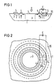
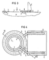
- FIGS. 1 and 2 A semiconductor body is shown in FIGS. 1 and 2, the base zone of which on the cathode side is designated by 1. For example, it is p-doped.
- An auxiliary emitter zone 2 is embedded in the surface of the base zone 1.
- the auxiliary emitter zone 2 is an annulus, which includes a light-sensitive area 3.
- the light-sensitive region is understood to mean that region which is intended for the incidence of light. The incident light is indicated by a thick arrow.
- the auxiliary emitter zone 2 has a pn junction, the inner edge of which is adjacent to the light-sensitive region 3 and is designated by 6. Its edge facing away from the light-sensitive area is designated by 7. Adjacent to the photosensitive region 3 there is a base electrode 4 on the base zone 1, which only contacts the base zone 1 and surrounds the photosensitive region 3.
- the base electrode 4 is, for example, also ring-shaped.
- the auxiliary emitter zone 2 is connected to an auxiliary emitter electrode 5, which is also ring-shaped.
- the auxiliary emitter electrode 5 contacts the auxiliary emitter zone 2 and the base zone 1 on the side facing the emitter zone 20 of the main thyristor.
- the outer edge 7 of the auxiliary emitter zone 2 is thus short-circuited.
- a capacitor C is connected between the electrodes 4 and 5. The capacitor therefore bridges the auxiliary emitter zone 2 in the direction from the photosensitive region 3 to the main emitter zone 20.
- a voltage current applied to the thyristor in the blocking direction generates a displacement current that comes from inside of the semiconductor body flows to the cathode side. This stream is symbolized by the thin upward arrows. A large part of this current flows through the electrode 4 into the capacitor C and charges it. A smaller part of the displacement current flows radially outwards under the auxiliary emitter zone 2 to the electrode 5. The current flowing to the electrode 5 biases the auxiliary emitter. Because a large part of the displacement current does not flow radially under the auxiliary emitter to the electrode 5 but instead into the capacitor, the displacement current, ie the du / dt at the thyristor, can be increased without the auxiliary thyristor igniting.
- SMD surface mounted device
- a typical area requirement of a capacitor of the above capacity is 2.0 x 1.2 mm2.
- the capacitor can also be integrated. can be applied, for example, with an oxide as a dielectric. In this case, the space requirement is greater.
- the capacitance of 8 nF it is around 0.2 cm2.
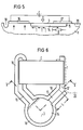
- FIGS. 3 and 4 An embodiment with a capacitor integrated on the thyristor is shown in FIGS. 3 and 4.
- the same or functionally identical parts as in FIGS. 1 and 2 have the same reference numerals.
- the base electrode 4 is connected to a conductor track 8, which is applied to an oxide layer 9 and lies in a gap in the auxiliary emitter electrode 5.
- the oxide layer 9, which can also be another insulating layer, insulates the conductor track 8 from the auxiliary emitter zone 2.
- the auxiliary emitter electrode 5 is connected to a contact finger 10, which is also on an insulating layer, e.g. an oxide layer 11 can be arranged.
- the mode of operation is the same as that mentioned in connection with FIGS. 1 and 2.
- the exemplary embodiments according to FIGS. 1 to 4 are characterized in that the light-sensitive area is the base zone 1 lying on the surface. However, as is known, the light-sensitive area can also be covered by the auxiliary emitter zone. Such an embodiment is shown in FIGS. 5 and 6.
- the auxiliary emitter zone is designated here by 14, the photosensitive region again by 3.
- the auxiliary emitter zone 14 is provided with an auxiliary emitter electrode 17 which also contacts the base zone 1.
- the base zone 1 is contacted with a base electrode 16 adjacent to the photosensitive region 3.
- the capacitor C is connected to the electrodes 16 and 17.
- a displacement current flowing out of the semiconductor body due to a du / dt load generates a current which is characterized by the thin, upward-pointing arrows. Most of the displacement current flows laterally under the emitter zone 14 or directly vertically to the electrode 16. The capacitor is thus charged in the specified polarity. A fraction of the displacement current flows laterally in the base zone below the auxiliary emitter zone 14 to the auxiliary emitter electrode 17 and from there to the main thyristor. Its path resistance is indicated by the dashed resistance symbol R.
- FIG. 6 5 is a section along the line V - V through FIG. 6.
- the auxiliary emitter zone 14 is provided with a strip-shaped extension 15 which extends radially to the zone 14.
- the length L of this extension determines the size of R for a given width.
- the extension is covered with a strip-shaped auxiliary emitter electrode 17. It also contacts the base zone 1 and lies opposite the emitter zone 20 of the main emitter.
- the base electrode 16 is also formed by a conductor strip which also extends essentially radially to the auxiliary emitter zone 14.
- the strips 16 and 17 are shaped such that an SMD capacitor can be mounted. However, they can also be shaped differently. Basically, the area of the strip 16 should be as small as possible.
- the contact 16 is surrounded by a trench 18.
- the trench 18 expediently also delimits the auxiliary emitter zone 14 and the long sides of the extension 15.
- the photo current generated under the zone 14 in the space charge zone is thus forced to flow under the extension 15.
- the trench can also extend to that side of the auxiliary emitter electrode which is opposite the base electrode 16.
- the photosensitivity is reduced until the capacitor C is charged. If it is charged, there is only the shunt caused by the auxiliary electrode between the auxiliary emitter zone 2 and the base zone 1.
Landscapes
- Thyristors (AREA)
- Light Receiving Elements (AREA)
Claims (7)
- Thyristor commandable par la lumière et comportant un corps semiconducteur, présentant les particularités suivantesa) le corps semiconducteur possède une zone photosensible (3), une zone de base (1), une zone d'émetteur auxiliaire (2;14) et une zone d'émetteur principal (20),b) la zone d'émetteur auxiliaire est placée en contact avec une électrode d'émetteur auxiliaire (5;17),c) l'électrode d'émetteur auxiliaire (5;17) est placée en contact, d'une part, avec la zone d'émetteur auxiliaire (2), et, d'autre part, avec la zone de base (1) sur la face située à l'opposé de la zone d'émetteur principale (20),caractérisé par une électrode de base (4), qui est disposée entre la zone photosensible (3) et la zone d'émetteur auxiliaire (2) et établit un contact avec la zone de base (1), et par le condensateur (C), qui est branché entre l'électrode de base (4) et l'électrode d'émetteur auxiliaire.
- Thyristor commandable par la lumière suivant la revendication 1, caractérisé par le fait que l'électrode de base (4) et la zone d'émetteur auxiliaire (2) possèdent une forme annulaire et entourent la zone photosensible (3).
- Thyristor commandable par la lumière et comportant un corps semiconducteur, présentant les particularités suivantesa) le corps semiconducteur possède une zone photosensible (3), une zone de base (1), une zone d'émetteur auxiliaire (2;14) et une zone d'émetteur principal (20),b) la zone d'émetteur auxiliaire est placée en contact avec une électrode d'émetteur auxiliaire (5;17),c) l'électrode d'émetteur auxiliaire (5;17) est placée en contact, d'une part, avec la zone d'émetteur auxiliaire (2), et, d'autre part, avec la zone de base (1) sur la face située à l'opposé de la zone d'émetteur principale (20),caractérisé par le fait que la zone photosensible (3) est recouverte par la zone d'émetteur auxiliaire (14), que l'électrode d'émetteur auxiliaire (17) et l'électrode de base sont agencées sous la forme de bandes et sont disposées radialement par rapport à la zone d'émetteur auxiliaire (14) et qu'un condensateur (C) est branché entre l'électrode de base et l'électrode d'émetteur auxiliaire.
- Thyristor suivant la revendication 3, caractérisé par le fait que la zone d'émetteur auxiliaire (14) possède un prolongement en forme de bande (15), que la zone d'émetteur auxiliaire, l'électrode de base (16) et les deux côtés longitudinaux du prolongement sont entourés par un sillon (18) qui est situé dans la zone de base (1) et est plus profond que la zone d'émetteur auxiliaire.
- Thyristor suivant l'une des revendications 1 à 5, caractérisé par le fait que le condensateur (C) est fixé sur le corps semiconducteur.
- Thyristor suivant la revendication 5, caractérisé par le fait que le condensateur (C) est un composant pouvant être monté sur une surface et est fixé, par ses bornes, directement sur l'électrode d'émetteur auxiliaire (17) et sur l'électrode de base (7).
- Thyristor suivant la revendication 5, caractérisé par le fait que le condensateur (C) est disposé de façon intégrée sur la surface du corps semiconducteur.
Applications Claiming Priority (2)
| Application Number | Priority Date | Filing Date | Title |
|---|---|---|---|
| DE3727820 | 1987-08-20 | ||
| DE3727820 | 1987-08-20 |
Publications (2)
| Publication Number | Publication Date |
|---|---|
| EP0304032A1 EP0304032A1 (fr) | 1989-02-22 |
| EP0304032B1 true EP0304032B1 (fr) | 1993-01-27 |
Family
ID=6334143
Family Applications (1)
| Application Number | Title | Priority Date | Filing Date |
|---|---|---|---|
| EP88113350A Expired - Lifetime EP0304032B1 (fr) | 1987-08-20 | 1988-08-17 | Thyristor commandé par la lumière |
Country Status (3)
| Country | Link |
|---|---|
| EP (1) | EP0304032B1 (fr) |
| JP (1) | JPH01120063A (fr) |
| DE (1) | DE3877858D1 (fr) |
Families Citing this family (1)
| Publication number | Priority date | Publication date | Assignee | Title |
|---|---|---|---|---|
| JP4175379B2 (ja) | 2006-04-25 | 2008-11-05 | 日本電気株式会社 | ファイル共有方法およびファイル共有システム |
Family Cites Families (4)
| Publication number | Priority date | Publication date | Assignee | Title |
|---|---|---|---|---|
| DE2458401C2 (de) * | 1974-12-10 | 1982-06-24 | Siemens AG, 1000 Berlin und 8000 München | Mit Licht steuerbarer Thyristor |
| DE2538549C2 (de) * | 1975-08-29 | 1985-06-13 | Siemens AG, 1000 Berlin und 8000 München | Mit Licht steuerbarer Thyristor |
| DE2715482C2 (de) * | 1977-04-06 | 1985-06-13 | Siemens AG, 1000 Berlin und 8000 München | Mit Licht steuerbarer Thyristor |
| US4489340A (en) * | 1980-02-04 | 1984-12-18 | Nippon Telegraph & Telephone Public Corporation | PNPN Light sensitive semiconductor switch with phototransistor connected across inner base regions |
-
1988
- 1988-08-17 EP EP88113350A patent/EP0304032B1/fr not_active Expired - Lifetime
- 1988-08-17 DE DE8888113350T patent/DE3877858D1/de not_active Expired - Fee Related
- 1988-08-19 JP JP63206220A patent/JPH01120063A/ja active Pending
Also Published As
| Publication number | Publication date |
|---|---|
| DE3877858D1 (de) | 1993-03-11 |
| JPH01120063A (ja) | 1989-05-12 |
| EP0304032A1 (fr) | 1989-02-22 |
Similar Documents
| Publication | Publication Date | Title |
|---|---|---|
| DE2625917A1 (de) | Halbleiteranordnung | |
| EP0039943B1 (fr) | Thyristor à courts-circuits d'émetteur contrôlables et procédé pour son fonctionnement | |
| DE2932152A1 (de) | Ueberspannungsschutz zum schutz von einheiten, die halbleiterbauelemente fuer kleine leistungen enthalten | |
| DE19653615A1 (de) | Leistungshalbleiterbauteil mit überlappender Feldplattenstruktur und Verfahren zu dessen Herstellung | |
| CH668505A5 (de) | Halbleiterbauelement. | |
| DE69302244T2 (de) | Halbleiter-Schutzkomponente | |
| DE2716874C2 (de) | Thyristor | |
| DE3521079C2 (fr) | ||
| DE3631136C2 (fr) | ||
| DE3401407C2 (fr) | ||
| DE2922301C2 (de) | Lichtsteuerbarer Thyristor und Verfahren zu seiner Herstellung | |
| DE3102851C2 (de) | PNPN-Halbleiterschalter | |
| EP0014435B1 (fr) | Thyristor commandé par transistor à effet de champ | |
| DE1216435B (de) | Schaltbares Halbleiterbauelement mit vier Zonen | |
| DE4022022A1 (de) | Hochspannungshalbleitervorrichtung | |
| EP0028798A2 (fr) | Thyristor à gachette amplificatrice et procédé pour son fonctionnement | |
| DE3502180A1 (de) | Festkoerperrelais | |
| EP0430133B1 (fr) | Dispositif semi-conducteur de puissance comportant des courts-circuits d'émetteur | |
| DE2915885C2 (de) | Thyristor mit Steuerung durch Feldeffekttransistor | |
| EP0304032B1 (fr) | Thyristor commandé par la lumière | |
| DE2329398B2 (de) | In Ruckwartsrichtung leitendes Thyristorbauelement | |
| EP0559945B1 (fr) | Dispositif semi-conducteur de puissance à extinction | |
| DE2425364A1 (de) | Gate-gesteuerter halbleitergleichrichter | |
| DE4439012A1 (de) | Zweirichtungsthyristor | |
| EP0310836A2 (fr) | Elément semi-conducteur avec une jonction pn planaire |
Legal Events
| Date | Code | Title | Description |
|---|---|---|---|
| PUAI | Public reference made under article 153(3) epc to a published international application that has entered the european phase |
Free format text: ORIGINAL CODE: 0009012 |
|
| AK | Designated contracting states |
Kind code of ref document: A1 Designated state(s): CH DE FR GB LI SE |
|
| 17P | Request for examination filed |
Effective date: 19890726 |
|
| 17Q | First examination report despatched |
Effective date: 19910411 |
|
| GRAA | (expected) grant |
Free format text: ORIGINAL CODE: 0009210 |
|
| AK | Designated contracting states |
Kind code of ref document: B1 Designated state(s): CH DE FR GB LI SE |
|
| REF | Corresponds to: |
Ref document number: 3877858 Country of ref document: DE Date of ref document: 19930311 |
|
| ET | Fr: translation filed | ||
| GBT | Gb: translation of ep patent filed (gb section 77(6)(a)/1977) |
Effective date: 19930401 |
|
| PGFP | Annual fee paid to national office [announced via postgrant information from national office to epo] |
Ref country code: GB Payment date: 19930714 Year of fee payment: 6 |
|
| PGFP | Annual fee paid to national office [announced via postgrant information from national office to epo] |
Ref country code: SE Payment date: 19930813 Year of fee payment: 6 |
|
| PGFP | Annual fee paid to national office [announced via postgrant information from national office to epo] |
Ref country code: FR Payment date: 19930819 Year of fee payment: 6 |
|
| PGFP | Annual fee paid to national office [announced via postgrant information from national office to epo] |
Ref country code: DE Payment date: 19931020 Year of fee payment: 6 |
|
| PGFP | Annual fee paid to national office [announced via postgrant information from national office to epo] |
Ref country code: CH Payment date: 19931116 Year of fee payment: 6 |
|
| PLBE | No opposition filed within time limit |
Free format text: ORIGINAL CODE: 0009261 |
|
| STAA | Information on the status of an ep patent application or granted ep patent |
Free format text: STATUS: NO OPPOSITION FILED WITHIN TIME LIMIT |
|
| 26N | No opposition filed | ||
| PG25 | Lapsed in a contracting state [announced via postgrant information from national office to epo] |
Ref country code: GB Effective date: 19940817 |
|
| PG25 | Lapsed in a contracting state [announced via postgrant information from national office to epo] |
Ref country code: SE Effective date: 19940818 |
|
| PG25 | Lapsed in a contracting state [announced via postgrant information from national office to epo] |
Ref country code: LI Effective date: 19940831 Ref country code: CH Effective date: 19940831 |
|
| EAL | Se: european patent in force in sweden |
Ref document number: 88113350.8 |
|
| GBPC | Gb: european patent ceased through non-payment of renewal fee |
Effective date: 19940817 |
|
| PG25 | Lapsed in a contracting state [announced via postgrant information from national office to epo] |
Ref country code: FR Effective date: 19950428 |
|
| REG | Reference to a national code |
Ref country code: CH Ref legal event code: PL |
|
| PG25 | Lapsed in a contracting state [announced via postgrant information from national office to epo] |
Ref country code: DE Effective date: 19950503 |
|
| EUG | Se: european patent has lapsed |
Ref document number: 88113350.8 |
|
| REG | Reference to a national code |
Ref country code: FR Ref legal event code: ST |