EP0304813B1 - Interface série - Google Patents
Interface série Download PDFInfo
- Publication number
- EP0304813B1 EP0304813B1 EP88113485A EP88113485A EP0304813B1 EP 0304813 B1 EP0304813 B1 EP 0304813B1 EP 88113485 A EP88113485 A EP 88113485A EP 88113485 A EP88113485 A EP 88113485A EP 0304813 B1 EP0304813 B1 EP 0304813B1
- Authority
- EP
- European Patent Office
- Prior art keywords
- control signals
- signal
- flip
- static
- circuit arrangement
- Prior art date
- Legal status (The legal status is an assumption and is not a legal conclusion. Google has not performed a legal analysis and makes no representation as to the accuracy of the status listed.)
- Expired - Lifetime
Links
Images
Classifications
-
- H—ELECTRICITY
- H04—ELECTRIC COMMUNICATION TECHNIQUE
- H04H—BROADCAST COMMUNICATION
- H04H40/00—Arrangements specially adapted for receiving broadcast information
- H04H40/18—Arrangements characterised by circuits or components specially adapted for receiving
- H04H40/27—Arrangements characterised by circuits or components specially adapted for receiving specially adapted for broadcast systems covered by groups H04H20/53 - H04H20/95
- H04H40/90—Arrangements characterised by circuits or components specially adapted for receiving specially adapted for broadcast systems covered by groups H04H20/53 - H04H20/95 specially adapted for satellite broadcast receiving
Definitions
- the invention relates to a circuit arrangement for evaluating control signals according to the preamble of claim 1.
- the invention has for its object to provide a circuit arrangement for evaluating control signals, which reliably separates the differently formed control signals and evaluates them for control purposes. This object is achieved in a circuit arrangement according to the preamble of claim 1 by the features specified in the characterizing part.
- static and dynamic control signals are static only over a relatively long period of time, but change their state when the command is changed, and this change can be confused with a dynamic state change.
- the dynamic changes in state behave like brief static changes, so that there is also a risk of confusion in this direction.
- the static states are first stored and the output of the memory is then used as a control signal. It is thereby achieved that a dynamic change of state has no influence on the can exercise the control signals obtained from the static control signals.
- the dynamic control signals are used to synchronize a flip-flop, so that this error is subsequently compensated for even in the event of incorrect synchronization by changing static control signals.
- the receiver for digital satellite broadcasting is intended to receive radio programs in accordance with the specifications of the radio transmission method in TV-SAT.
- the nesting of the programs in a frame structure and the accommodation of additional program information in special service frames and special service superframes, as well as in an additional information frame are described in DE-OS 33 080 25 or the technical guidelines ARD / ZDF No. 3R1 "Digital Satellite” Broadcasting (DSR) - Specifications of the radio transmission method in TV-SAT ", published by the IRT Institute for Broadcasting Technology, described in more detail.
- a special service bit and two additional information bits are transmitted in addition to the other data.
- Sixty-four main frames are combined into a special service frame SA for the special service bits and into an additional information frame for the additional information bits.
- part of the available data is reserved for scale factors and another part for program information PI.
- the program accompanying information PI relates to the programs whose samples have previously been transmitted.
- the number of available bits is not sufficient to be able to transmit program information for all channels in the additional information frame. Only with stereo programs in which the program information is common to both channels is it possible to accommodate complete program information in an additional information frame. If, on the other hand, the channels are used individually, i.e.
- the program information is transmitted alternately for the mono channels, the assignment being defined such that the program information for the left mono channel of the program begins with the start of a special service frame 1 is transmitted.
- each subsequent additional information frame of an odd number or each subsequent additional information frame of even number must be evaluated after the start of the special service superframe.
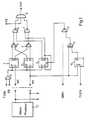
- a data processor 13 is shown, at one control output control signals M1 and at the other control output control signals M2 occur.
- the status of the static control signals M1S and M2S indicates which operating mode is present.
- the coding is selected so that in stereo both outputs are at logic L, in two-tone broadcasts both outputs are at logic H, with mono-left M1S on logic H and M2S on logic L and on mono right M1 on logic L and M2S on logic H.
- a dynamic signal M1D which briefly changes the state of M1, is output when it has been determined by the data processor that the synchronous word for the special service superframe has been correctly recognized.
- the signals are used to set a time window for program information in the "Mono" operating mode so that only the program information for the switched-on channel is evaluated and the others are suppressed.
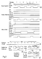
- FIG. 2 the signals being shown there on different stretched scales.
- the additional information frames as well as the special service frames each contain 64 bits.
- Eight special service frames result in a special service superframe, as shown in FIG. 2a.
- such signals are shown as continuous signals that occur regularly in the additional information frame.
- One is a signal G9, which appears during the duration of the ninth clock, and a signal G89N, which appears during the duration of the 18th and 19th clock.
- a window signal FE is also shown, through which the data containing the program accompanying information can be extracted from the data stream.
- the program accompanying information for the stereo programs is transmitted in each additional information frame. It is therefore permissible to evaluate the PI bits occurring during the duration of the signal FE in each additional information frame.
- control signals M1, M2 are at logic L, as a result of which both flip-flops 1,2 produce logic L at their outputs via their outputs and the downstream NOR logic gates 3,4. Accordingly, the NAND gates 6, 7 are blocked and logically generate H. Das at the AND gate 8 Signal FE present at a third input is now switched through during each additional information frame.
- the “mono-left” operating mode is illustrated below the representation for stereo operation in FIG. 2d.
- the static control signals are correspondingly at M1 at logic H and M2 at logic L.
- the data processor After recognizing the synchronous word of the special service superframe SAÜ, the data processor briefly inverts the control signals and in this way emits a dynamic control signal M1D, which is used to select the window should continue to be used, in which the program information for the left mono channel is contained.
- the static control signals are present at the inputs of the flip-flop 1 and the flip-flop 2 before the event of the dynamic control signals M1D and are stored beforehand.
- a clock T32N, which is continuously present, and a signal G9, which is present in the additional information frame during the ninth bit, are used via the AND logic element 5 to be taken over into the memories.
- the corresponding pulse diagram is shown in FIG. 2e
Landscapes
- Physics & Mathematics (AREA)
- Astronomy & Astrophysics (AREA)
- General Physics & Mathematics (AREA)
- Engineering & Computer Science (AREA)
- Signal Processing (AREA)
- Circuits Of Receivers In General (AREA)
- Manufacturing Of Electric Cables (AREA)
- Time-Division Multiplex Systems (AREA)
- Input Circuits Of Receivers And Coupling Of Receivers And Audio Equipment (AREA)
- Diaphragms For Electromechanical Transducers (AREA)
- Microcomputers (AREA)
- Debugging And Monitoring (AREA)
- Test And Diagnosis Of Digital Computers (AREA)
- Testing, Inspecting, Measuring Of Stereoscopic Televisions And Televisions (AREA)
- Communication Control (AREA)
- Synchronisation In Digital Transmission Systems (AREA)
Claims (3)
- Dispositif de circuit pour l'exploitation de signaux de commande, émis par un processeur de données, qui se composent de signaux de commande statiques et de signaux de commande dynamiques superposés aux signaux de commande statiques, caractérisé en ce qu'il est prévu au moins une mémoire (1, 2) à laquelle sont amenés les signaux de commande statiques (M1S, M2S) et qu'il est prévu une autre mémoire (9) qui est synchronisée par le signal de commande dynamique (M1D).
- Dispositif de circuit selon la revendication 1, les signaux de commande statiques (M1S, M2S) servent à l'identification d'un mode et les signaux de commande dynamiques (M1D) servent à la synchronisation d'un circuit d'exploitation pour des données spécifiques du mode à partir d'un flux de données série, en particulier pour l'exploitation d'informations de programme pour la radiodiffusion numérique par sattelite, caractérisé en ce qu'un premier et un second signal de commande statique (M1S, M2S) sont amenés à deux flip-flops (1, 2) qui mettent en mémoire les états des signaux de commande à des moments prédéterminés, qu'il est prévu un détecteur de flancs (10, 11) pour les signaux de commande dynamiques (M1D) dont le signal de sortie est amené à une entrée de mise à un (R) d'un flip-flop (9) commuté comme diviseur de fréquence (9) qui est rythmé avec le même cycle (T32N) que les deux autres flip-flops (1, 2) et que les sorties des flip-flops (1, 2) sont enchaînées par un circuit combinatoire (3, 4, 6, 7, 8) avec un signal de fenêtre (FE).
- Dispositif de circuit selon la revendication 2, caractérisé en ce que le cycle (T32N) pour les flip-flops (1, 2, 9) est enchaîné avec un signal auxiliaire (G9) qui existe dans une première période et le signal dynamique (M1D) est enchaîné avec un deuxième signal auxiliaire (G89) et que le premier (G9) et le second signal auxiliaire (G89) sont décalés dans le temps l'un par rapport à l'autre.
Priority Applications (1)
| Application Number | Priority Date | Filing Date | Title |
|---|---|---|---|
| AT88113485T ATE96589T1 (de) | 1987-08-28 | 1988-08-19 | Serielle schnittstelle. |
Applications Claiming Priority (2)
| Application Number | Priority Date | Filing Date | Title |
|---|---|---|---|
| DE3728793 | 1987-08-28 | ||
| DE19873728793 DE3728793A1 (de) | 1987-08-28 | 1987-08-28 | Schaltungsanordnung zur auswertung von aus einem datenprozessor ausgegebene steuersignale |
Publications (3)
| Publication Number | Publication Date |
|---|---|
| EP0304813A2 EP0304813A2 (fr) | 1989-03-01 |
| EP0304813A3 EP0304813A3 (fr) | 1991-04-10 |
| EP0304813B1 true EP0304813B1 (fr) | 1993-10-27 |
Family
ID=6334723
Family Applications (1)
| Application Number | Title | Priority Date | Filing Date |
|---|---|---|---|
| EP88113485A Expired - Lifetime EP0304813B1 (fr) | 1987-08-28 | 1988-08-19 | Interface série |
Country Status (5)
| Country | Link |
|---|---|
| EP (1) | EP0304813B1 (fr) |
| JP (1) | JP2950834B2 (fr) |
| AT (1) | ATE96589T1 (fr) |
| DE (2) | DE3728793A1 (fr) |
| HK (1) | HK124494A (fr) |
Families Citing this family (11)
| Publication number | Priority date | Publication date | Assignee | Title |
|---|---|---|---|---|
| JP3076587B2 (ja) * | 1990-05-31 | 2000-08-14 | ナカミチ株式会社 | チェンジャー型ディスク再生装置 |
| EP0614178A3 (fr) * | 1993-03-05 | 1994-10-12 | Nakamichi Corp | Lecteur à disques avec dispositif de transport pour disques compact. |
| JP3183744B2 (ja) * | 1993-03-05 | 2001-07-09 | ナカミチ株式会社 | チェンジャ機能を備えたディスク再生装置 |
| US5508994A (en) * | 1993-03-05 | 1996-04-16 | Nakamichi Corporation | Disk player with compact arrangement of a reader and disk storage magazine |
| JPH06259865A (ja) * | 1993-03-05 | 1994-09-16 | Nakamichi Corp | ディスク再生装置 |
| JPH06259869A (ja) * | 1993-03-05 | 1994-09-16 | Nakamichi Corp | ディスク再生装置 |
| JPH06259864A (ja) * | 1993-03-05 | 1994-09-16 | Nakamichi Corp | ディスク再生装置 |
| JP2596255Y2 (ja) * | 1993-03-23 | 1999-06-07 | ナカミチ株式会社 | ディスク再生装置 |
| US5544148A (en) * | 1993-05-20 | 1996-08-06 | Nakamichi Corporation | Compact configuration disk player |
| JPH06349186A (ja) * | 1993-06-03 | 1994-12-22 | Nakamichi Corp | ディスク再生装置 |
| JP4741024B1 (ja) * | 2010-01-27 | 2011-08-03 | シャープ株式会社 | 画像形成装置 |
Family Cites Families (3)
| Publication number | Priority date | Publication date | Assignee | Title |
|---|---|---|---|---|
| JPS60117939A (ja) * | 1983-11-30 | 1985-06-25 | Matsushita Electric Works Ltd | 情報伝送方式 |
| JPS6170827A (ja) * | 1984-09-14 | 1986-04-11 | Yamatake Honeywell Co Ltd | 通信装置 |
| SE458972B (sv) * | 1984-06-04 | 1989-05-22 | Yamatake Honeywell Co Ltd | Dialogfoerfarande samt anordning foer genomfoerande av foerfarandet |
-
1987
- 1987-08-28 DE DE19873728793 patent/DE3728793A1/de not_active Withdrawn
-
1988
- 1988-08-19 AT AT88113485T patent/ATE96589T1/de active
- 1988-08-19 EP EP88113485A patent/EP0304813B1/fr not_active Expired - Lifetime
- 1988-08-19 DE DE88113485T patent/DE3885204D1/de not_active Expired - Fee Related
- 1988-08-26 JP JP63210867A patent/JP2950834B2/ja not_active Expired - Fee Related
-
1994
- 1994-11-10 HK HK124494A patent/HK124494A/xx not_active IP Right Cessation
Also Published As
| Publication number | Publication date |
|---|---|
| ATE96589T1 (de) | 1993-11-15 |
| HK124494A (en) | 1994-11-18 |
| JPS6471338A (en) | 1989-03-16 |
| EP0304813A2 (fr) | 1989-03-01 |
| DE3728793A1 (de) | 1989-03-09 |
| EP0304813A3 (fr) | 1991-04-10 |
| DE3885204D1 (de) | 1993-12-02 |
| JP2950834B2 (ja) | 1999-09-20 |
Similar Documents
| Publication | Publication Date | Title |
|---|---|---|
| DE2560513C2 (de) | Verfahren zum authorisierten Empfang von im Fernsehmodus ausgesandten Informationen und Vorrichtung zur Durchführung des Verfahrens | |
| DE4008385C2 (fr) | ||
| DE2838104A1 (de) | Speicherkreis fuer einen tuner | |
| DE2726277A1 (de) | Abtastsignaldetektor | |
| DE69124840T2 (de) | Speicherplatzzuordnung für mehrere Speicherbausteine | |
| EP0304813A2 (fr) | Interface série | |
| DE3743586C2 (fr) | ||
| DE3209530C2 (de) | Textdarstellungseinrichtung für ein Textverarbeitungssystem | |
| DE68913919T2 (de) | Hochfrequenz-Taktimpulszähler. | |
| DE2752996A1 (de) | Digitale multiplexiervorrichtung fuer plesiochrone bitfolgen | |
| DE2627713A1 (de) | Schaltungsanordnung zur feststellung der identitaet zwischen zwei bit-impulszuegen | |
| DE3001388C2 (de) | Frequenzteiler | |
| DE3838940A1 (de) | Schaltung mit testfunktionsschaltung | |
| DE2505388A1 (de) | Verfahren und anordnung zur logarithmischen umwandlung eines messwertes | |
| DE3311896A1 (de) | Frequenzbestimmungseinrichtung | |
| DE2556486A1 (de) | Abstimmschaltung fuer hochfrequenzempfangsgeraete | |
| DE3438369A1 (de) | Digitales nachrichtenuebertragungssystem | |
| DE1799029A1 (de) | Oszillografische schriftzeichenwiedergabevorrichtung | |
| EP0021084B1 (fr) | Mémoire intégrée monolithique à semi-conducteurs | |
| DE4422784C2 (de) | Schaltungsanordnung mit wenigstens einer Schaltungseinheit wie einem Register, einer Speicherzelle, einer Speicheranordnung oder dergleichen | |
| DE3688338T2 (de) | Am-stereo-empfaenger. | |
| DE69110793T2 (de) | Zeitvielfachmultiplexiereinrichtung. | |
| DE2449984C2 (de) | Verriegelungsschaltung | |
| DE3332847C2 (de) | Oszillograf | |
| DE4303806C2 (de) | Programmierbarer Frequenzzähler |
Legal Events
| Date | Code | Title | Description |
|---|---|---|---|
| PUAI | Public reference made under article 153(3) epc to a published international application that has entered the european phase |
Free format text: ORIGINAL CODE: 0009012 |
|
| AK | Designated contracting states |
Kind code of ref document: A2 Designated state(s): AT BE CH DE ES FR GB GR IT LI LU NL SE |
|
| PUAL | Search report despatched |
Free format text: ORIGINAL CODE: 0009013 |
|
| 17P | Request for examination filed |
Effective date: 19901231 |
|
| AK | Designated contracting states |
Kind code of ref document: A3 Designated state(s): AT BE CH DE ES FR GB GR IT LI LU NL SE |
|
| 17Q | First examination report despatched |
Effective date: 19921009 |
|
| GRAA | (expected) grant |
Free format text: ORIGINAL CODE: 0009210 |
|
| AK | Designated contracting states |
Kind code of ref document: B1 Designated state(s): AT BE CH DE ES FR GB GR IT LI LU NL SE |
|
| PG25 | Lapsed in a contracting state [announced via postgrant information from national office to epo] |
Ref country code: SE Effective date: 19931027 Ref country code: GR Free format text: LAPSE BECAUSE OF FAILURE TO SUBMIT A TRANSLATION OF THE DESCRIPTION OR TO PAY THE FEE WITHIN THE PRESCRIBED TIME-LIMIT Effective date: 19931027 Ref country code: ES Free format text: THE PATENT HAS BEEN ANNULLED BY A DECISION OF A NATIONAL AUTHORITY Effective date: 19931027 Ref country code: BE Effective date: 19931027 |
|
| REF | Corresponds to: |
Ref document number: 96589 Country of ref document: AT Date of ref document: 19931115 Kind code of ref document: T |
|
| ITF | It: translation for a ep patent filed | ||
| REF | Corresponds to: |
Ref document number: 3885204 Country of ref document: DE Date of ref document: 19931202 |
|
| GBT | Gb: translation of ep patent filed (gb section 77(6)(a)/1977) |
Effective date: 19931109 |
|
| ET | Fr: translation filed | ||
| PLBE | No opposition filed within time limit |
Free format text: ORIGINAL CODE: 0009261 |
|
| PG25 | Lapsed in a contracting state [announced via postgrant information from national office to epo] |
Ref country code: LU Free format text: LAPSE BECAUSE OF NON-PAYMENT OF DUE FEES Effective date: 19940831 |
|
| 26N | No opposition filed | ||
| REG | Reference to a national code |
Ref country code: GB Ref legal event code: 746 Effective date: 19970904 |
|
| PGFP | Annual fee paid to national office [announced via postgrant information from national office to epo] |
Ref country code: AT Payment date: 19980825 Year of fee payment: 11 |
|
| PGFP | Annual fee paid to national office [announced via postgrant information from national office to epo] |
Ref country code: CH Payment date: 19980826 Year of fee payment: 11 |
|
| PGFP | Annual fee paid to national office [announced via postgrant information from national office to epo] |
Ref country code: NL Payment date: 19980827 Year of fee payment: 11 |
|
| PG25 | Lapsed in a contracting state [announced via postgrant information from national office to epo] |
Ref country code: AT Free format text: LAPSE BECAUSE OF NON-PAYMENT OF DUE FEES Effective date: 19990819 |
|
| PG25 | Lapsed in a contracting state [announced via postgrant information from national office to epo] |
Ref country code: LI Free format text: LAPSE BECAUSE OF NON-PAYMENT OF DUE FEES Effective date: 19990831 Ref country code: CH Free format text: LAPSE BECAUSE OF NON-PAYMENT OF DUE FEES Effective date: 19990831 |
|
| PG25 | Lapsed in a contracting state [announced via postgrant information from national office to epo] |
Ref country code: NL Free format text: LAPSE BECAUSE OF NON-PAYMENT OF DUE FEES Effective date: 20000301 |
|
| REG | Reference to a national code |
Ref country code: CH Ref legal event code: PL |
|
| NLV4 | Nl: lapsed or anulled due to non-payment of the annual fee |
Effective date: 20000301 |
|
| REG | Reference to a national code |
Ref country code: FR Ref legal event code: D6 |
|
| REG | Reference to a national code |
Ref country code: GB Ref legal event code: IF02 |
|
| PGFP | Annual fee paid to national office [announced via postgrant information from national office to epo] |
Ref country code: GB Payment date: 20020624 Year of fee payment: 15 |
|
| PGFP | Annual fee paid to national office [announced via postgrant information from national office to epo] |
Ref country code: FR Payment date: 20020823 Year of fee payment: 15 |
|
| PGFP | Annual fee paid to national office [announced via postgrant information from national office to epo] |
Ref country code: DE Payment date: 20020904 Year of fee payment: 15 |
|
| PG25 | Lapsed in a contracting state [announced via postgrant information from national office to epo] |
Ref country code: GB Free format text: LAPSE BECAUSE OF NON-PAYMENT OF DUE FEES Effective date: 20030819 |
|
| PG25 | Lapsed in a contracting state [announced via postgrant information from national office to epo] |
Ref country code: DE Free format text: LAPSE BECAUSE OF NON-PAYMENT OF DUE FEES Effective date: 20040302 |
|
| GBPC | Gb: european patent ceased through non-payment of renewal fee |
Effective date: 20030819 |
|
| PG25 | Lapsed in a contracting state [announced via postgrant information from national office to epo] |
Ref country code: FR Free format text: LAPSE BECAUSE OF NON-PAYMENT OF DUE FEES Effective date: 20040430 |
|
| REG | Reference to a national code |
Ref country code: FR Ref legal event code: ST |
|
| PG25 | Lapsed in a contracting state [announced via postgrant information from national office to epo] |
Ref country code: IT Free format text: LAPSE BECAUSE OF NON-PAYMENT OF DUE FEES;WARNING: LAPSES OF ITALIAN PATENTS WITH EFFECTIVE DATE BEFORE 2007 MAY HAVE OCCURRED AT ANY TIME BEFORE 2007. THE CORRECT EFFECTIVE DATE MAY BE DIFFERENT FROM THE ONE RECORDED. Effective date: 20050819 |