EP0304814B1 - Dispositif de synchronisation - Google Patents
Dispositif de synchronisation Download PDFInfo
- Publication number
- EP0304814B1 EP0304814B1 EP88113487A EP88113487A EP0304814B1 EP 0304814 B1 EP0304814 B1 EP 0304814B1 EP 88113487 A EP88113487 A EP 88113487A EP 88113487 A EP88113487 A EP 88113487A EP 0304814 B1 EP0304814 B1 EP 0304814B1
- Authority
- EP
- European Patent Office
- Prior art keywords
- control signals
- circuit
- data
- circuit arrangement
- accordance
- Prior art date
- Legal status (The legal status is an assumption and is not a legal conclusion. Google has not performed a legal analysis and makes no representation as to the accuracy of the status listed.)
- Expired - Lifetime
Links
- 230000000737 periodic effect Effects 0.000 claims abstract 5
- 102220139344 rs886055905 Human genes 0.000 claims description 5
- 230000003068 static effect Effects 0.000 claims 1
- 230000001360 synchronised effect Effects 0.000 description 9
- 238000011156 evaluation Methods 0.000 description 4
- 230000005540 biological transmission Effects 0.000 description 2
- 238000010586 diagram Methods 0.000 description 2
- 230000004308 accommodation Effects 0.000 description 1
- 238000011161 development Methods 0.000 description 1
- 230000018109 developmental process Effects 0.000 description 1
- 238000000034 method Methods 0.000 description 1
Images

Classifications
-
- H—ELECTRICITY
- H04—ELECTRIC COMMUNICATION TECHNIQUE
- H04J—MULTIPLEX COMMUNICATION
- H04J3/00—Time-division multiplex systems
- H04J3/02—Details
- H04J3/06—Synchronising arrangements
- H04J3/0602—Systems characterised by the synchronising information used
- H04J3/0605—Special codes used as synchronising signal
Definitions
- the invention relates to a circuit arrangement for synchronizing a data processor with a serial data stream according to the preamble of claim 1.
- the invention has for its object to provide a circuit arrangement for synchronizing a data processor so that different control signals can be supplied via a single control port.
- control signals are first obtained, the first of which each identify a data sequence belonging together and the second indicate the occurrence of a data sequence which corresponds to setpoints, for example a synchronous data word.
- These separate control signals are then merged and linked by a logic circuit so that the length of time forms the criterion for which of the two control signals is present.
- This solution is particularly advantageous for control signals, one of which occurs less frequently but always at the same time as the other.
- the receiver for digital satellite broadcasting is intended to receive radio programs in accordance with the specifications of the radio transmission method in TV-Sat.
- the nesting of the programs in a frame structure and the accommodation of additional program information in special service frames and special service superframes are described in more detail in DE-OS 33 08 025.
- the special service superframe SAÜ comprises eight special service frames SA, each of which consists of a synchronous word and program type information for currently two programs, ie program 1 + 2, program 3 + 4 ... program 15 + 16.
- the special service superframe SAÜ begins with the special service frame SA, which contains the program type information for program 1 and program 2 after the synchronization word.
- the synchronous word which indicates the new beginning of the special service superframe SAÜ with the first special service frame SA differs slightly in bit structure from the synchronous words which each initiate the second to eighth special service frame SA.
- the bits used to represent the synchronous words and program type information are those in the main frame A according to the above. Specifications transmitted special service bit. These are evaluated by a data processor. However, in addition to the calculations to be carried out, the data processor is also unable to monitor synchronous words occurring in the data stream. This task is performed by an evaluation circuit which, based on the evaluated signals, transmits corresponding control signals to the data processor, which thereby recognizes the beginning of certain data sequences.
- the control signals emitted by the evaluation circuit are first control signals A which identify the end of data words that belong together, in this case those of 8 bits in length, and second control signals PR1 which identify the start of the program type information for program 1.
- the first control signals are to arrive at the data processor as INTR1 and the second as INTR2.
- An additional control signal INTR3 should then reach the data processor when the evaluation circuit cannot recognize any synchronous signals SYOKN.
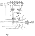
- the circuit shown in Fig. 1 is able to combine these three control signals emitted by the evaluation circuit so that they can be routed to the data processor as signals with different pulse length changes via a single control line.
- This clock is passed to a divider 1, which can perform a frequency division in the ratio between 21 and 26.
- divider 1 is initially set to a defined state by evaluating an SA synchronous word, in that it is loaded with the value 1 by a load command LD1.
- a signal A is now generated with every eighth clock T32N, which signal arrives at a control input of the data processor via an logic element 4 as INTR1.
- a signal INTR2 appears which comprises twice the pulse length as the signal INTR1.
- This signal is processed by the data processor in such a way that it first causes IRTN1 is to take over data and, after taking over the data, the information received by INTR2 is supplemented that this is data for program 1.
Landscapes
- Computer Networks & Wireless Communication (AREA)
- Signal Processing (AREA)
- Engineering & Computer Science (AREA)
- Synchronisation In Digital Transmission Systems (AREA)
- Glass Compositions (AREA)
- Selective Calling Equipment (AREA)
- Input Circuits Of Receivers And Coupling Of Receivers And Audio Equipment (AREA)
- Information Transfer Systems (AREA)
- Logic Circuits (AREA)
- Electronic Switches (AREA)
- Control Of Indicators Other Than Cathode Ray Tubes (AREA)
- Time-Division Multiplex Systems (AREA)
- Details Of Television Scanning (AREA)
Claims (6)
- Dispositif de circuit pour la synchronisation d'un processeur de données avec un flux de données sériel, caractérisé en ce qu'un circuit d'exploitation (1, 2), qui est prévu pour une séquence de données qui vont ensemble qui sont contenues dans le flux de données, donne les premiers signaux de commande périodiques (A), qu'il est prévu un circuit comparateur qui compare les séquences de données à une séquence de valeurs de consigne prédéterminée et qui les amène à un circuit de mise en mémoire (3) qui donne des seconds signaux de commande périodiques (B) décalés dans le temps par rapport aux premiers signaux de commande et que les premiers et les seconds signaux de commande (A, B) sont amenés au processeur de données comme signaux de commande (INTR1, INTR2) par l'intermédiaire d'un circuit d'enchaînement (4).
- Dispositif de circuit selon la revendication 1, caractérisé en ce que le circuit de mise en mémoire (3) est un flip-flop qui décale les seconds signaux de commande (B) de la longueur d'impulsion des premiers (A).
- Dispositif de circuit selon la revendication 1 ou 2, caractérisé en ce que le circuit d'enchaînement (4) est un circuit OU.
- Dispositif de circuit selon l'une ou plusieurs des revendications 1 à 3, caractérisé en ce que les premiers signaux de commande périodiques (A) sont obtenus par des signaux d'horloge T32N qui sont amenés à un diviseur de fréquence (1) dont le rapport de division correspond au nombre des bits qui font partie ensemble d'un mot de données.
- Dispositif de circuit selon la revendication 4, la séquence de données étant intégrée à au moins une structure de cadre biétagée, caractérisé en ce que les seconds signaux de commande périodiques (B) sont également obtenus par des signaux d'horloge T32N qui sont amenées à un diviseur de fréquence (1) dont le rapport de division correspond au nombre des mots de données qui vont ensemble et qui sont contenus dans un cadre SA et que les signaux de sortie (F16-23) du diviseur (1) sont enchaînés aux seconds signaux de commande (PR1).
- Dispositif de circuit selon l'une ou plusieurs des revendications 1 à 4, caractérisé en ce qu'il est prévu un autre circuit comparateur qui compare les séquences de données à une séquence de valeurs de consigne prédéterminée et qui donne des troisièmes signaux de commande statiques (SYOKN) et que les troisièmes signaux de commande (SYOKN) sont enchaînés, après retard par un élément de retard (5), comme signaux de commande (C) aux premiers (A) et aux seconds signaux de commande (B) par le circuit d'enchaînement (4) et sont amenés au processeur de données comme (INTR3).
Priority Applications (1)
| Application Number | Priority Date | Filing Date | Title |
|---|---|---|---|
| AT88113487T ATE96591T1 (de) | 1987-08-28 | 1988-08-19 | Schaltungsanordnung zur synchronisation. |
Applications Claiming Priority (2)
| Application Number | Priority Date | Filing Date | Title |
|---|---|---|---|
| DE3728781 | 1987-08-28 | ||
| DE19873728781 DE3728781A1 (de) | 1987-08-28 | 1987-08-28 | Schaltungsanordnung zur synchronisation |
Publications (3)
| Publication Number | Publication Date |
|---|---|
| EP0304814A2 EP0304814A2 (fr) | 1989-03-01 |
| EP0304814A3 EP0304814A3 (en) | 1990-08-16 |
| EP0304814B1 true EP0304814B1 (fr) | 1993-10-27 |
Family
ID=6334713
Family Applications (1)
| Application Number | Title | Priority Date | Filing Date |
|---|---|---|---|
| EP88113487A Expired - Lifetime EP0304814B1 (fr) | 1987-08-28 | 1988-08-19 | Dispositif de synchronisation |
Country Status (6)
| Country | Link |
|---|---|
| EP (1) | EP0304814B1 (fr) |
| JP (1) | JP2703277B2 (fr) |
| AT (1) | ATE96591T1 (fr) |
| DE (2) | DE3728781A1 (fr) |
| ES (1) | ES2046259T3 (fr) |
| HK (1) | HK124694A (fr) |
Families Citing this family (1)
| Publication number | Priority date | Publication date | Assignee | Title |
|---|---|---|---|---|
| DE4216574A1 (de) * | 1992-05-20 | 1993-11-25 | Thomas Dr Blaffert | Verfahren zur Erzeugung und Verarbeitung von Synchronsignalen sowie eine Vorrichtung zur Durchführung des Verfahrens |
Family Cites Families (2)
| Publication number | Priority date | Publication date | Assignee | Title |
|---|---|---|---|---|
| DE1183119B (de) * | 1963-10-15 | 1964-12-10 | Telefunken Patent | Verfahren zur Datenuebertragung, bei dem die Information in einzelnen Bloecken uebertragen wird, deren Anfang durch jeweils vor Blockbeginn am Empfangsort eintreffende Synchronisiersignale gekennzeichnet wird |
| JPS5630340A (en) * | 1979-08-20 | 1981-03-26 | Sony Corp | Digital signal transmitting method |
-
1987
- 1987-08-28 DE DE19873728781 patent/DE3728781A1/de not_active Withdrawn
-
1988
- 1988-08-19 EP EP88113487A patent/EP0304814B1/fr not_active Expired - Lifetime
- 1988-08-19 ES ES198888113487T patent/ES2046259T3/es not_active Expired - Lifetime
- 1988-08-19 AT AT88113487T patent/ATE96591T1/de active
- 1988-08-19 DE DE88113487T patent/DE3885205D1/de not_active Expired - Fee Related
- 1988-08-26 JP JP63210865A patent/JP2703277B2/ja not_active Expired - Lifetime
-
1994
- 1994-11-10 HK HK124694A patent/HK124694A/xx not_active IP Right Cessation
Also Published As
| Publication number | Publication date |
|---|---|
| DE3885205D1 (de) | 1993-12-02 |
| JP2703277B2 (ja) | 1998-01-26 |
| ATE96591T1 (de) | 1993-11-15 |
| HK124694A (en) | 1994-11-18 |
| EP0304814A2 (fr) | 1989-03-01 |
| ES2046259T3 (es) | 1994-02-01 |
| EP0304814A3 (en) | 1990-08-16 |
| JPS6471353A (en) | 1989-03-16 |
| DE3728781A1 (de) | 1989-03-09 |
Similar Documents
| Publication | Publication Date | Title |
|---|---|---|
| DE2011353C3 (de) | Verfahren zur Informationsübertragung und Informationsübertragungssystem zum Durchführen desselben | |
| DE3102447C2 (fr) | ||
| DE2406740C2 (de) | Schaltungsanordnung zur Steuerung des Datentransfers zwischen einem Datenprozessor und einer Fernverarbeitungseinrichtung | |
| EP0262478B1 (fr) | Procédé de synchronisation de trames d'un central d'un réseau de télécommunication à multiplexage temporel MIC | |
| DE2726277A1 (de) | Abtastsignaldetektor | |
| DE3780406T2 (de) | Verfahren und anordnung zur kodierung und dekodierung binaerer information. | |
| EP0190554A1 (fr) | Procédé et arrangement pour la commutation d'un dispostif commandé par horloge avec plusieurs états de fonctionnement | |
| DE2838757A1 (de) | Schnittstellenschaltung fuer zeitmultiplexleitungen von nachrichtenvermittlungsanlagen | |
| DE3743586C2 (fr) | ||
| EP0023331B1 (fr) | Circuit pour la synchronisation d'un dispositif subordonné, en particulier un poste d'abonné numérique par un dispositif d'ordre supérieur, en particulier un central de communication numérique d'un réseau de télécommunication MIC | |
| DE2752996A1 (de) | Digitale multiplexiervorrichtung fuer plesiochrone bitfolgen | |
| DE69604273T2 (de) | Verfahren und Apparat zur Synchronisierung von Empfangsdaten in Zeitschlitzen | |
| EP0304813B1 (fr) | Interface série | |
| DE2225462A1 (de) | Verfahren und Einrichtung zur Mittelwertbildung der von einem Vorwärts-Rückwärtssignalgeber her anliegenden Signale | |
| DE2433885A1 (de) | Verfahren und vorrichtung zum synchronisieren eines testinstruments auf ein digitales system | |
| DE60030932T2 (de) | Suche des optimalen Abtastzeitpunktes in einem TDMA Paketübertragungssystem | |
| EP0304814B1 (fr) | Dispositif de synchronisation | |
| DE2641700A1 (de) | Taktueberwachung in digitalsystemen | |
| DE60130594T2 (de) | SDH Testvorrichtung und SDH Testverfahren | |
| DE69934886T2 (de) | System und Verfahren zur zuverlässigen Umschaltung zwischen redundanten Takten | |
| EP0304815B1 (fr) | Circuit de détection et/ou de contrôle de mots de synchronisation contenus dans une transmission en série de données | |
| DE2454517A1 (de) | Verfahren und vorrichtung zur fehlerkorrektur in uebertragungseinrichtungen fuer digitale daten | |
| DE102004010562B4 (de) | Schnittstellenvorrichtung und Verfahren zur Synchronisation von Daten | |
| DE1766413B1 (de) | Synchronisation eines Zeitmultiplex-UEbertragungssystems | |
| DE1221671B (de) | Anordnung zum Empfang pulscodemodulierter Zeitteilungsmultiplex-Signale |
Legal Events
| Date | Code | Title | Description |
|---|---|---|---|
| PUAI | Public reference made under article 153(3) epc to a published international application that has entered the european phase |
Free format text: ORIGINAL CODE: 0009012 |
|
| AK | Designated contracting states |
Kind code of ref document: A2 Designated state(s): AT BE CH DE ES FR GB GR IT LI LU NL SE |
|
| PUAL | Search report despatched |
Free format text: ORIGINAL CODE: 0009013 |
|
| AK | Designated contracting states |
Kind code of ref document: A3 Designated state(s): AT BE CH DE ES FR GB GR IT LI LU NL SE |
|
| 17P | Request for examination filed |
Effective date: 19901231 |
|
| 17Q | First examination report despatched |
Effective date: 19921009 |
|
| GRAA | (expected) grant |
Free format text: ORIGINAL CODE: 0009210 |
|
| AK | Designated contracting states |
Kind code of ref document: B1 Designated state(s): AT BE CH DE ES FR GB GR IT LI LU NL SE |
|
| PG25 | Lapsed in a contracting state [announced via postgrant information from national office to epo] |
Ref country code: SE Effective date: 19931027 Ref country code: GR Free format text: LAPSE BECAUSE OF FAILURE TO SUBMIT A TRANSLATION OF THE DESCRIPTION OR TO PAY THE FEE WITHIN THE PRESCRIBED TIME-LIMIT Effective date: 19931027 |
|
| REF | Corresponds to: |
Ref document number: 96591 Country of ref document: AT Date of ref document: 19931115 Kind code of ref document: T |
|
| ITF | It: translation for a ep patent filed | ||
| REF | Corresponds to: |
Ref document number: 3885205 Country of ref document: DE Date of ref document: 19931202 |
|
| GBT | Gb: translation of ep patent filed (gb section 77(6)(a)/1977) |
Effective date: 19931109 |
|
| REG | Reference to a national code |
Ref country code: ES Ref legal event code: FG2A Ref document number: 2046259 Country of ref document: ES Kind code of ref document: T3 |
|
| ET | Fr: translation filed | ||
| PLBE | No opposition filed within time limit |
Free format text: ORIGINAL CODE: 0009261 |
|
| STAA | Information on the status of an ep patent application or granted ep patent |
Free format text: STATUS: NO OPPOSITION FILED WITHIN TIME LIMIT |
|
| PG25 | Lapsed in a contracting state [announced via postgrant information from national office to epo] |
Ref country code: LU Free format text: LAPSE BECAUSE OF NON-PAYMENT OF DUE FEES Effective date: 19940831 |
|
| 26N | No opposition filed | ||
| REG | Reference to a national code |
Ref country code: GB Ref legal event code: 746 Effective date: 19970904 |
|
| PGFP | Annual fee paid to national office [announced via postgrant information from national office to epo] |
Ref country code: GB Payment date: 19980703 Year of fee payment: 11 |
|
| PGFP | Annual fee paid to national office [announced via postgrant information from national office to epo] |
Ref country code: FR Payment date: 19980814 Year of fee payment: 11 |
|
| PGFP | Annual fee paid to national office [announced via postgrant information from national office to epo] |
Ref country code: BE Payment date: 19980824 Year of fee payment: 11 |
|
| PGFP | Annual fee paid to national office [announced via postgrant information from national office to epo] |
Ref country code: AT Payment date: 19980825 Year of fee payment: 11 |
|
| PGFP | Annual fee paid to national office [announced via postgrant information from national office to epo] |
Ref country code: CH Payment date: 19980826 Year of fee payment: 11 |
|
| PGFP | Annual fee paid to national office [announced via postgrant information from national office to epo] |
Ref country code: NL Payment date: 19980827 Year of fee payment: 11 |
|
| PGFP | Annual fee paid to national office [announced via postgrant information from national office to epo] |
Ref country code: ES Payment date: 19980828 Year of fee payment: 11 Ref country code: DE Payment date: 19980828 Year of fee payment: 11 |
|
| PG25 | Lapsed in a contracting state [announced via postgrant information from national office to epo] |
Ref country code: GB Free format text: LAPSE BECAUSE OF NON-PAYMENT OF DUE FEES Effective date: 19990819 Ref country code: AT Free format text: LAPSE BECAUSE OF NON-PAYMENT OF DUE FEES Effective date: 19990819 |
|
| PG25 | Lapsed in a contracting state [announced via postgrant information from national office to epo] |
Ref country code: ES Free format text: LAPSE BECAUSE OF NON-PAYMENT OF DUE FEES Effective date: 19990820 |
|
| PG25 | Lapsed in a contracting state [announced via postgrant information from national office to epo] |
Ref country code: LI Free format text: LAPSE BECAUSE OF NON-PAYMENT OF DUE FEES Effective date: 19990831 Ref country code: CH Free format text: LAPSE BECAUSE OF NON-PAYMENT OF DUE FEES Effective date: 19990831 Ref country code: BE Free format text: LAPSE BECAUSE OF NON-PAYMENT OF DUE FEES Effective date: 19990831 |
|
| BERE | Be: lapsed |
Owner name: DEUTSCHE THOMSON-BRANDT G.M.B.H. Effective date: 19990831 |
|
| PG25 | Lapsed in a contracting state [announced via postgrant information from national office to epo] |
Ref country code: NL Free format text: LAPSE BECAUSE OF NON-PAYMENT OF DUE FEES Effective date: 20000301 |
|
| GBPC | Gb: european patent ceased through non-payment of renewal fee |
Effective date: 19990819 |
|
| REG | Reference to a national code |
Ref country code: CH Ref legal event code: PL |
|
| PG25 | Lapsed in a contracting state [announced via postgrant information from national office to epo] |
Ref country code: FR Free format text: LAPSE BECAUSE OF NON-PAYMENT OF DUE FEES Effective date: 20000428 |
|
| NLV4 | Nl: lapsed or anulled due to non-payment of the annual fee |
Effective date: 20000301 |
|
| PG25 | Lapsed in a contracting state [announced via postgrant information from national office to epo] |
Ref country code: DE Free format text: LAPSE BECAUSE OF NON-PAYMENT OF DUE FEES Effective date: 20000601 |
|
| REG | Reference to a national code |
Ref country code: FR Ref legal event code: ST |
|
| REG | Reference to a national code |
Ref country code: ES Ref legal event code: FD2A Effective date: 20000911 |
|
| PG25 | Lapsed in a contracting state [announced via postgrant information from national office to epo] |
Ref country code: IT Free format text: LAPSE BECAUSE OF NON-PAYMENT OF DUE FEES;WARNING: LAPSES OF ITALIAN PATENTS WITH EFFECTIVE DATE BEFORE 2007 MAY HAVE OCCURRED AT ANY TIME BEFORE 2007. THE CORRECT EFFECTIVE DATE MAY BE DIFFERENT FROM THE ONE RECORDED. Effective date: 20050819 |