EP0305295A2 - Metallbeschichtungsstruktur für keramische Materialien aus Aluminiumnitrid und Verfahren zu ihrer Herstellung - Google Patents
Metallbeschichtungsstruktur für keramische Materialien aus Aluminiumnitrid und Verfahren zu ihrer Herstellung Download PDFInfo
- Publication number
- EP0305295A2 EP0305295A2 EP88402161A EP88402161A EP0305295A2 EP 0305295 A2 EP0305295 A2 EP 0305295A2 EP 88402161 A EP88402161 A EP 88402161A EP 88402161 A EP88402161 A EP 88402161A EP 0305295 A2 EP0305295 A2 EP 0305295A2
- Authority
- EP
- European Patent Office
- Prior art keywords
- layer
- layer structure
- metallization
- metallization layer
- producing
- Prior art date
- Legal status (The legal status is an assumption and is not a legal conclusion. Google has not performed a legal analysis and makes no representation as to the accuracy of the status listed.)
- Granted
Links
Images



Classifications
-
- C—CHEMISTRY; METALLURGY
- C04—CEMENTS; CONCRETE; ARTIFICIAL STONE; CERAMICS; REFRACTORIES
- C04B—LIME, MAGNESIA; SLAG; CEMENTS; COMPOSITIONS THEREOF, e.g. MORTARS, CONCRETE OR LIKE BUILDING MATERIALS; ARTIFICIAL STONE; CERAMICS; REFRACTORIES; TREATMENT OF NATURAL STONE
- C04B41/00—After-treatment of mortars, concrete, artificial stone or ceramics; Treatment of natural stone
- C04B41/009—After-treatment of mortars, concrete, artificial stone or ceramics; Treatment of natural stone characterised by the material treated
-
- H—ELECTRICITY
- H10—SEMICONDUCTOR DEVICES; ELECTRIC SOLID-STATE DEVICES NOT OTHERWISE PROVIDED FOR
- H10W—GENERIC PACKAGES, INTERCONNECTIONS, CONNECTORS OR OTHER CONSTRUCTIONAL DETAILS OF DEVICES COVERED BY CLASS H10
- H10W20/00—Interconnections in chips, wafers or substrates
- H10W20/40—Interconnections external to wafers or substrates, e.g. back-end-of-line [BEOL] metallisations or vias connecting to gate electrodes
- H10W20/41—Interconnections external to wafers or substrates, e.g. back-end-of-line [BEOL] metallisations or vias connecting to gate electrodes characterised by their conductive parts
- H10W20/425—Barrier, adhesion or liner layers
-
- C—CHEMISTRY; METALLURGY
- C04—CEMENTS; CONCRETE; ARTIFICIAL STONE; CERAMICS; REFRACTORIES
- C04B—LIME, MAGNESIA; SLAG; CEMENTS; COMPOSITIONS THEREOF, e.g. MORTARS, CONCRETE OR LIKE BUILDING MATERIALS; ARTIFICIAL STONE; CERAMICS; REFRACTORIES; TREATMENT OF NATURAL STONE
- C04B41/00—After-treatment of mortars, concrete, artificial stone or ceramics; Treatment of natural stone
- C04B41/45—Coating or impregnating, e.g. injection in masonry, partial coating of green or fired ceramics, organic coating compositions for adhering together two concrete elements
- C04B41/52—Multiple coating or impregnating multiple coating or impregnating with the same composition or with compositions only differing in the concentration of the constituents, is classified as single coating or impregnation
-
- C—CHEMISTRY; METALLURGY
- C04—CEMENTS; CONCRETE; ARTIFICIAL STONE; CERAMICS; REFRACTORIES
- C04B—LIME, MAGNESIA; SLAG; CEMENTS; COMPOSITIONS THEREOF, e.g. MORTARS, CONCRETE OR LIKE BUILDING MATERIALS; ARTIFICIAL STONE; CERAMICS; REFRACTORIES; TREATMENT OF NATURAL STONE
- C04B41/00—After-treatment of mortars, concrete, artificial stone or ceramics; Treatment of natural stone
- C04B41/80—After-treatment of mortars, concrete, artificial stone or ceramics; Treatment of natural stone of only ceramics
- C04B41/81—Coating or impregnation
- C04B41/89—Coating or impregnation for obtaining at least two superposed coatings having different compositions
-
- H—ELECTRICITY
- H05—ELECTRIC TECHNIQUES NOT OTHERWISE PROVIDED FOR
- H05K—PRINTED CIRCUITS; CASINGS OR CONSTRUCTIONAL DETAILS OF ELECTRIC APPARATUS; MANUFACTURE OF ASSEMBLAGES OF ELECTRICAL COMPONENTS
- H05K1/00—Printed circuits
- H05K1/02—Details
- H05K1/03—Use of materials for the substrate
- H05K1/0306—Inorganic insulating substrates, e.g. ceramic, glass
-
- H—ELECTRICITY
- H05—ELECTRIC TECHNIQUES NOT OTHERWISE PROVIDED FOR
- H05K—PRINTED CIRCUITS; CASINGS OR CONSTRUCTIONAL DETAILS OF ELECTRIC APPARATUS; MANUFACTURE OF ASSEMBLAGES OF ELECTRICAL COMPONENTS
- H05K3/00—Apparatus or processes for manufacturing printed circuits
- H05K3/38—Improvement of the adhesion between the insulating substrate and the metal
-
- H—ELECTRICITY
- H10—SEMICONDUCTOR DEVICES; ELECTRIC SOLID-STATE DEVICES NOT OTHERWISE PROVIDED FOR
- H10W—GENERIC PACKAGES, INTERCONNECTIONS, CONNECTORS OR OTHER CONSTRUCTIONAL DETAILS OF DEVICES COVERED BY CLASS H10
- H10W72/00—Interconnections or connectors in packages
- H10W72/50—Bond wires
- H10W72/531—Shapes of wire connectors
- H10W72/536—Shapes of wire connectors the connected ends being ball-shaped
-
- H—ELECTRICITY
- H10—SEMICONDUCTOR DEVICES; ELECTRIC SOLID-STATE DEVICES NOT OTHERWISE PROVIDED FOR
- H10W—GENERIC PACKAGES, INTERCONNECTIONS, CONNECTORS OR OTHER CONSTRUCTIONAL DETAILS OF DEVICES COVERED BY CLASS H10
- H10W72/00—Interconnections or connectors in packages
- H10W72/50—Bond wires
- H10W72/531—Shapes of wire connectors
- H10W72/5363—Shapes of wire connectors the connected ends being wedge-shaped
-
- H—ELECTRICITY
- H10—SEMICONDUCTOR DEVICES; ELECTRIC SOLID-STATE DEVICES NOT OTHERWISE PROVIDED FOR
- H10W—GENERIC PACKAGES, INTERCONNECTIONS, CONNECTORS OR OTHER CONSTRUCTIONAL DETAILS OF DEVICES COVERED BY CLASS H10
- H10W72/00—Interconnections or connectors in packages
- H10W72/851—Dispositions of multiple connectors or interconnections
- H10W72/874—On different surfaces
- H10W72/884—Die-attach connectors and bond wires
-
- H—ELECTRICITY
- H10—SEMICONDUCTOR DEVICES; ELECTRIC SOLID-STATE DEVICES NOT OTHERWISE PROVIDED FOR
- H10W—GENERIC PACKAGES, INTERCONNECTIONS, CONNECTORS OR OTHER CONSTRUCTIONAL DETAILS OF DEVICES COVERED BY CLASS H10
- H10W90/00—Package configurations
- H10W90/701—Package configurations characterised by the relative positions of pads or connectors relative to package parts
- H10W90/731—Package configurations characterised by the relative positions of pads or connectors relative to package parts of die-attach connectors
- H10W90/734—Package configurations characterised by the relative positions of pads or connectors relative to package parts of die-attach connectors between a chip and a stacked insulating package substrate, interposer or RDL
-
- H—ELECTRICITY
- H10—SEMICONDUCTOR DEVICES; ELECTRIC SOLID-STATE DEVICES NOT OTHERWISE PROVIDED FOR
- H10W—GENERIC PACKAGES, INTERCONNECTIONS, CONNECTORS OR OTHER CONSTRUCTIONAL DETAILS OF DEVICES COVERED BY CLASS H10
- H10W90/00—Package configurations
- H10W90/701—Package configurations characterised by the relative positions of pads or connectors relative to package parts
- H10W90/751—Package configurations characterised by the relative positions of pads or connectors relative to package parts of bond wires
- H10W90/754—Package configurations characterised by the relative positions of pads or connectors relative to package parts of bond wires between a chip and a stacked insulating package substrate, interposer or RDL
-
- Y—GENERAL TAGGING OF NEW TECHNOLOGICAL DEVELOPMENTS; GENERAL TAGGING OF CROSS-SECTIONAL TECHNOLOGIES SPANNING OVER SEVERAL SECTIONS OF THE IPC; TECHNICAL SUBJECTS COVERED BY FORMER USPC CROSS-REFERENCE ART COLLECTIONS [XRACs] AND DIGESTS
- Y10—TECHNICAL SUBJECTS COVERED BY FORMER USPC
- Y10T—TECHNICAL SUBJECTS COVERED BY FORMER US CLASSIFICATION
- Y10T428/00—Stock material or miscellaneous articles
- Y10T428/12—All metal or with adjacent metals
- Y10T428/12014—All metal or with adjacent metals having metal particles
- Y10T428/12028—Composite; i.e., plural, adjacent, spatially distinct metal components [e.g., layers, etc.]
- Y10T428/12049—Nonmetal component
- Y10T428/12056—Entirely inorganic
-
- Y—GENERAL TAGGING OF NEW TECHNOLOGICAL DEVELOPMENTS; GENERAL TAGGING OF CROSS-SECTIONAL TECHNOLOGIES SPANNING OVER SEVERAL SECTIONS OF THE IPC; TECHNICAL SUBJECTS COVERED BY FORMER USPC CROSS-REFERENCE ART COLLECTIONS [XRACs] AND DIGESTS
- Y10—TECHNICAL SUBJECTS COVERED BY FORMER USPC
- Y10T—TECHNICAL SUBJECTS COVERED BY FORMER US CLASSIFICATION
- Y10T428/00—Stock material or miscellaneous articles
- Y10T428/12—All metal or with adjacent metals
- Y10T428/12493—Composite; i.e., plural, adjacent, spatially distinct metal components [e.g., layers, joint, etc.]
- Y10T428/12535—Composite; i.e., plural, adjacent, spatially distinct metal components [e.g., layers, joint, etc.] with additional, spatially distinct nonmetal component
- Y10T428/12576—Boride, carbide or nitride component
-
- Y—GENERAL TAGGING OF NEW TECHNOLOGICAL DEVELOPMENTS; GENERAL TAGGING OF CROSS-SECTIONAL TECHNOLOGIES SPANNING OVER SEVERAL SECTIONS OF THE IPC; TECHNICAL SUBJECTS COVERED BY FORMER USPC CROSS-REFERENCE ART COLLECTIONS [XRACs] AND DIGESTS
- Y10—TECHNICAL SUBJECTS COVERED BY FORMER USPC
- Y10T—TECHNICAL SUBJECTS COVERED BY FORMER US CLASSIFICATION
- Y10T428/00—Stock material or miscellaneous articles
- Y10T428/31504—Composite [nonstructural laminate]
- Y10T428/31536—Including interfacial reaction product of adjacent layers
Definitions
- the present invention generally relates to a metallization for aluminum nitride ceramics having properties of a low thermal expansion and a high thermal conductivity. More particularly, the present invention relates to a metallization layer structure formed on aluminum nitride ceramics and a method of producing the metallization layer structure on the aluminum nitride ceramics.
- alumina (Al2O3) ceramics or a material of an oxide system such as glass containing silicon dioxide (SiO2) as a major component, are used as structural elements of various electronic devices such as packages of semiconductor integrated circuit devices.
- a metallization is employed such that a metallization layer is formed on alumina ceramics or glass of the oxide system.
- the metallization layer functions as an adhesive layer, so that structural parts can be fixedly fastened to alumina ceramics or glass of the oxide system.
- chromium (Cr), titanium (Ti) or aluminum is used as a material for the metallization with respect to alumina ceramics or glass of the oxide system.
- Structural parts are mounted on the metallization layer formed alumina ceramics or glass of the oxide system, and are then soldered or brazed.
- the above metallization has been disclosed in the Japanese Laid-Open Patent Application Nos.79910/1978, 207691/1984 and 57997/1985, for example.
- AlN ceramics aluminum nitride (AlN) ceramics as ceramics having properties of a small thermal expansion coefficient and a high thermal conductivity, compared with Al2O3 ceramics.
- the thermal conductivity of AlN ceramics is also smaller than that of glass of the SiO2 system.
- AlN ceramics has the thermal expansion coefficient of 4 x 10 ⁇ 6/°C, which is about half the thermal expansion coefficient of Al2O3 ceramics, or 7 x 10 ⁇ 6/°C.
- the thermal conductivity of AlN ceramics is three to eight times that of Al2O3 ceramics, and is also more than one thousand times as large as that of SiO2 glass.
- the Cr, Ti or Al metallization layer does not have a sufficient adhesive strength with respect to AlN ceramics of the non-oxide system. Therefore, the conventional metallization layer may be broken away from AlN ceramics. This lead to degradation in a hermetic seal of a package, for example.
- a general object of the present invention is to provide a novel and useful metallization layer structure formed on aluminum nitride ceramics and a method of producing the metallization layer structure in which the disadvantages of the prior art are overcome.
- a more specific object of the present invention is to provide a metallization layer structure formed on aluminum nitride ceramics and a method of producing the metallization layer structure having a sufficient adhesive strength.
- Another object of the present invention is to provide a metallization layer structure formed on aluminum nitride ceramics and a method of producing the metallization layer structure capable of providing an improved reliability of fastening of structural parts with respect to AlN ceramics.
- a metallization layer structure formed on AlN ceramics including the following layer structures.
- An intermediate layer is formed on an aluminum nitride ceramics base.
- the intermediate layer contains aluminum titanium nitride.
- a titanium layer is formed on the aluminum titanium nitride layer.
- a heat-resistant metallic layer is formed on the titanium layer.
- a metallic layer for facilitating soldering or brazing is formed on the heat-resistant metallic layer.
- a method of producing the above metallization layer structure including the steps of forming a titanium layer on an aluminum nitride ceramics base; forming a heat-resistant metallic layer on the titanium layer; forming a metallic layer on the heat-resistant metallic layer; subjecting the laminated layers to a heat treatment at a temperature within a predetermined range sufficient to generate an aluminum titanium nitride layer between the aluminum nitride ceramics base and the titanium layer.
- a further object of the present invention is to provide a method of producing a patterned metallization layer structure on aluminum nitride ceramics.
- the above further object of the present invention is attained by a method comprising the steps of forming a titanium layer on an aluminum nitride ceramics base; forming a heat-resistant metallic layer on the titanium layer; forming a metallic layer on the heat-resistant metallic layer; subjecting the laminated layers to a first heat treatment at a temperature lower than a temperature sufficient to form an aluminum titanium nitride layer between the aluminum nitride ceramics base and the titanium layer; patterning the laminated layers by etching; and subjecting the patterned layers to a second heat treatment at a temperature within a range sufficient to generate the aluminum titanium nitride layer between the aluminum nitride ceramics base and the patterned titanium layer.
- FIGS.1A through 1D A description is given of a preferred embodiment of the present invention with reference to FIGS.1A through 1D.
- a titanium (Ti) thin film layer 12 is formed on an aluminum nitride (AlN) ceramics base 11 by a conventional process such as conventional vacuum evaporation or sputtering.
- the AlN ceramics base 11 may be produced by a conventional process comprising the steps of forming an AlN powder to obtain a body having a desired shape, sintering the formed AlN base and burning the sintered AlN base.
- An AlN powder can be obtained by a method of directly nitrifying Al (2Al + N2 ⁇ 2AlN), a method of reducing carbon with respect to an aluminum compound such as Al2O3 and Al(OH)3 (Al2O3 + 3C + N2 ⁇ 2AlN + 3CO), a gas phase reaction method of reacting a halogenide compound of Al and hydrogen nitride (NH3).
- the AlN ceramics base 11 may be a single layer structure or a multilayer structure where a plurality of AlN plates are elevationally laminated.
- the Ti thin film layer 12 must have a thickness of at least 0.1 [ ⁇ m], preferably 0.5 [um] in order to cover convex and recess portions on the surface of the AlN ceramics base 11 to thus obtain a flat top surface thereof.
- a temperature to be set during the step for forming the Ti thin film layer 12 may be within a range of 200 to 250 [°C].
- a heat-resistant metallic layer 13 made of a heat-resistant metallic material such as tungsten (W) and molybdenum (Mo) is formed on top of the Ti thin film layer 12 by a conventional method such as vacuum evaporation and sputtering.
- the heat-resistant metallic layer 13 may be 1 to 5 [ ⁇ m] in thickness.
- a nickel (Ni) layer 14 having a thickness of 0.5 to 2.0 [ ⁇ m] is formed on top of the heat-resistant metallic layer 13 by a conventional method such as vacuum evaporation and sputtering.
- the layer structure of FIG.1C is heated into a non-oxiding atmosphere, preferably a reducing atmosphere such as a hydrogen gas.
- the heat treatment is carried out at a temperature within a range of 850 to 1000 [°C] for 40 [min].
- an intermediate layer 15 having a composition of aluminum titanium nitride Al x Ti 1-x N
- Al x Ti 1-x N aluminum titanium nitride
- This temperature range set during the heat treatment is a very important factor for producing the AlTiN intermediate layer 15, as described in detail later.
- the AlTiN intermediate layer 15 may be equal to or smaller than 1000 [ ⁇ ] in thickness.
- a metallization layer 100 made up of the AlTiN layer 15, the Ti thin film layer 12, the heat-resistant metallic layer 13, and the Ni layer 14 is formed on the AlN ceramics base 11.
- the presence of the AlTiN intermediate layer 15 contributes to improving the adhesive strength of the metallization layer 100.
- the Ni layer 14 is a layer necessary for fastening a member such as a metallic member to the AlN ceramics base 11 by soldering or brazing using silver.
- the heat-resistant metallic layer 13 is provided for the purpose of preventing the interdiffusion between the Ti thin film layer 12 and the Ni layer 14. It is to be noted that in case where the interdiffusion between the Ti thin film layer 12 and the Ni layer 14 occurs, the AlTiN intermediate layer 15 cannot be produced. Therefore, in such a case, it is impossible to obtain a metallization layer having an increased adhesive strength.
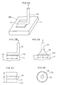
- FIGS.2A through 2C are with respect to an L-shaped tensile strength test
- FIGS.3A and 3B are with respect to an elevational tensile strength test.
- a plurality of samples shown in FIGS.2A through 2C were used in the test.
- a pad 110 of each of the samples is a patterned metallization layer, which can be obtained by a method described in detail later.
- the pad 110 having a size of 2.0 [mm2] was used in the test.
- a tinning copper wire 16 of an L-shaped cross section was soldered on the pad 110 with a PbSn solder in the state where a peripheral portion of the wire 16 makes contact with the pad 110.
- the wire 16 was 0.80 [mm] in diameter.
- the solder used in the test had a melting point of approximately 200 [°C].
- a solder portion is indicated by a reference numeral 17.
- the wire 16 was tensed in a direction indicated by an arrow, and a force necessary for the pad 110 to be broken away was measured. In the test, samples shown in FIGS.3A and 3B were also used.
- a tinning copper wire 18 having a diameter of 0.80 [mm] was soldered on the pad 110 so that an end thereof makes contact with the pad 110.
- the solder used in the test had a melting point of approximately 200 [°C].
- a solder portion is indicated by a reference numeral 19.
- the wire 18 was tensed in a direction of an arrow, and a force necessary for the pad 110 to be broken away was measured.
- FIG.4 shows the measurement results, where a broken line I is with respect to the L-shaped tensile test shown in FIGS.2A through 2C, and a solid line II is with respect to the vertical tensile test shown in FIGS.3A and 3B.
- a horizontal direction of the graph denotes a heat treatment temperature [°C]
- a vertical direction thereof denotes a force [kg/mm2] necessary for pad 11 to be broken away, which can be defined as an adhesive strength.
- Measured values of the strength with respect to the L-shaped tensile test and the vertical tensile test are plotted with symbols ⁇ and o, respectively.
- the curved lines I and II are obtained by appropriately tracing the symbols ⁇ and o, respectively.
- the adhesive strength measured at a heat treatment temperature equal to or lower than approximately 810 [°C] has a value equal to or smaller than 1.5 [kg/mm2].
- the heat treatment temperature is equal to 850 [°C]
- the measured adhesive strength is definitely more than 1.5 [kg/mm2].
- the heat treatment temperature was equal to 950 [°C]
- the measured adhesive strength was equal to 2.0 [kg/mm2]. It has been confirmed that although not shown in the graph, this value of the adhesive strength, 2.0 [kg/mm2] is substantially kept up to a temperature of approximately 1100 [°C] or over.
- the heat treatment should not be performed at a temperature more than about 1100 [°C]. It may be therefore concluded that it is preferable to carry out the heat treatment within a temperature range of 850 to 1000 [°C].
- the layer structure shown in FIG.1C is subjected to the heat treatment within the above temperature range, the metallization layer structure shown in FIG.1D can be obtained.
- the presence of the AlTiN intermediate layer 15 contributes to improving the adhesive strength of the metallization layer formed on the AlN ceramics base 11. In other words, if the layer structure of FIG.1C is subjected to the heat treatment without the above temperature range, the AlTiN intermediate layer 15 cannot be effectively produced.
- the presence of the AlTiN intermediate layer 15 can be confirmed by etching using a mixed acid containing a fluorine acid and a phosphoric acid. If the AlTiN intermediate layer 15 has not been produced, the surface of the AlN ceramics base 11 becomes exposed with a relatively short etching time. On the other hand, if the AlTiN intermediate layer 15 has been produced, an extremely long time is taken to obtain the exposed surface of the AlN ceramics base 11.
- the AlN ceramics base 11 is subjected to a low-temperature heat treatment at a temperature of 700 to 900 [°C] in a non-oxiding atmosphere, preferably a reducing atmosphere such as a hydrogen gas. Then the metallization layer 100 is subjected to a conventional patterning process in which an etching liquid containing a mixed acid of a fluorine acid and a phosphoric acid is used.
- the above low-temperature heat treatment allows some Ti atoms in the Ti thin film layer 12 to be diffused into the AlN ceramics layer 11, so that a strong coupling between the AlN ceramics base 11 and the Ti thin film layer 12 can be established. For this reason, it is preferable to perform the patterning step after the low-temperature heat treatment is carried out. Additionally, if the high-temperature heat treatment using a temperature of 850 to 1000 [°C] is performed without carrying out the low-temperature heat treatment for the layer structure of FIG.1C, a very long etching time is taken to etch the AlTiN intermediate layer 15. As a result, the trilayer structure on the AlTiN intermediate layer 15 may be over-etched, and thereby the adhesive strength of the metallization layer 100 may be reduced. The high-temperature heat treatment must be performed after the patterning step.
- a semiconductor device shown in FIGS.6A through 6C is a device obtained by applying the present invention to the device disclosed in the United States Patent No.4,698,663, the assignee of which is the same as the assignee of the present invention.
- the illustrated semiconductor device generally includes a semiconductor element 21 such as a silicon chip, an AlN ceramics base 22, a cap 23 and a heatsink member 24.
- a plurality of minute leads 25 extend outwardly from a periphery of a top face 21a and a polyimide resin layer 26.
- the semiconductor chip 21 is placed face downward on a multilevel interconnection layer 27 which is formed on top of the AlN ceramics base 22.
- the semiconductor chip 21 is electrically and mechanically coupled to the multilevel interconnection layer 27 without the use of wires.
- a metal 29 such as Mo and W is filled into the via holes 28 and is metallized.
- Patterned metallization layers 30 each having the same structure as that shown in FIG.5C are formed on the bottom surface of the AlN ceramics base 22.
- Each of the patterned metallization layers 30 is provided for the respective pins 35, and acts as an adhesive layer for fastening pins 35 to the AlN ceramics base 22.
- the pins 35 are soldered on the respective metallization layers 30. As described before, the presence of the metallization layers 30 can provide an improved adhesive strength.
- a patterned metallization layer 31 having a layer structure identical to that shown in FIG.5C is formed on a peripheral portion of the top surface of the AlN ceramics base 22.
- the patterned metallization layer 31 acts as an adhesive layer which can provide an improved adhesive strength and an improved hermetical seal.
- the cap 23 are fixedly soldered on the AlN ceramics base 22, so that the semiconductor chip 21 can be hermetically sealed and packaged. Further, the semiconductor chip 21 are soldered on bottom surfaces of the cap 23 and the heatsink member 24 by a solder 29.
- a metallization layer as shown in FIG.1D may be provided on bottom surface portions of the heatsink member 24 which correspond to positions of the cap 23 and heatsink member 24.
- the above semiconductor device may be fabricated as follows. To begin with, the AlN ceramics base 22 is formed as the aforementioned process. Next, the via holes 28 are formed into the AlN ceramics base 22. Then a metal powder of Mo, W or the like is filled into the via holes 28. Then the AlN ceramics base 22 is sintered, so that the metal powder is sintered. Thereafter, the layer structure shown in FIG.1C is formed on each of the top and bottom surfaces of the AlN ceramics base 22. Then, the formed layer structures are subjected to the low-temperature heat treatment and then patterning process in the processes described previously.
- the patterned layer is further subjected to the high-temperature heat treatment described before, so that the patterned metallization layers 30 and 31 each having the same structure as that shown in FIG.5C are formed. Then pins 35 are soldered on the corresponding patterned metallization layers 30.
- the multilayer interconnection layer 27 is formed on the top surface of the AlN ceramics base 22. Thereafter, the semiconductor chip 21 is mounted on top of the multilayer interconnection layer 27. Then a preformed solder is provided on top of the semiconductor chip 21 and then the cap 23 is placed so that a lower portion thereof is placed on the patterned metallization layer 31, and an upper portion thereof engages with the peripheral portion of the semiconductor chip 21 on which the preformed solder is formed. Thereafter, the heatsink member 24 is mounted as shown in FIG.6B. Then the device is subjected to the heat treatment where a temperature is set equal to 300 t0 330 [°C].
- FIG.7 is another semiconductor device using the metallization layers provided by the present invention.
- the pins 35 are mounted on the metallization films 30 formed on the AlN ceramics base 22.
- a cap 36 is mounted on the metallization layer 31 formed on the peripheral portion of the top surface of the AlN ceramics base 22. As shown, the cap 36 is separated from the semiconductor chip 21, and therefore stresses produced in soldered portions may be simplified, compared to the semiconductor device of FIGS.6A through 6C where the cap 23 engages directly with the semiconductor chip 21.
- FIG.8 shows yet another semiconductor device using the metallization layers 30 and 31 by the present invention.
- a cap 37 mounted on the metallization film 31 has an elevational portion 37a, and therefore the pressure tight of the cap 37 against the heatsink member 24 can be improved.
- patterned metallization layers 42 each identical to the layer structure of FIG.5C are formed on a bottom (or top) surface of an AlN ceramics base 41.
- a plurality of straight pins 43 are soldered on the patterned metallization layers 42.
- a reference numeral 44 indicates a solder portion formed around an end of the pin 43.
- a seal member 45 made of glass is formed on the patterned metallization layers 42.
- a cap 46 is fixedly mounted on the metallization layer 42 through the seal member 45.
- a semiconductor chip (silicon chip, for example) 47 is fixedly mounted on the patterned metallization layer 42.
- a bonding pad formed on a surface of the semiconductor chip 47 is connected to the corresponding patterned metallization layer 42 by a bonding wire 48. In place of wire bonding, tape automatic bonding may be used.
- the semiconductor chip 47 is hermetically sealed by the cap 46.
- FIG.10 shows a variation of the semiconductor device of FIG.8.
- the device of FIG.10 has pins 49, end portions of which extend horizontally.
- Other elements of the device of FIG.10 are the same as those shown in FIG.9.
- FIG.11 shows a still further example of applications of the present invention.
- An AlN ceramics base 51 is made up of laminated base portions 51a and 51b. Each of the base portions 51a and 51b has via holes, which are filled with a metal 54.
- the via hole metal 54 in the upper base portion 51a may be connected to the corresponding via hole metal 54 in the lower base portion 51b by a pattern 55 formed in an interface therebetween.
- On the bottom surface of the AlN ceramics base 51 there are formed patterned metallization layers 52, on which pins 56 are soldered by a solder 57. Also, patterned metallization layers 53 are formed on the top surface of the AlN ceramics base 51.
- a semiconductor chip 60 is mounted on the patterned metallization layer 53, which is connected to the corresponding metallization layer 53 by a bonding wire 61.
- the metallization layer to which the bonding wire is connected is also connected to the via hole metal 54 formed into the upper base portion 51a.
- the semiconductor chip 60 is hermetically sealed by a cap 59 soldered on the patterned metallization layer 53 by a solder 58.
- the multilayer AlN ceramics base 51 having the multilayer structure may be applied to the semiconductor devices shown in FIGS.6A, 6 and 7.
Landscapes
- Chemical & Material Sciences (AREA)
- Engineering & Computer Science (AREA)
- Ceramic Engineering (AREA)
- Materials Engineering (AREA)
- Structural Engineering (AREA)
- Organic Chemistry (AREA)
- Ceramic Products (AREA)
- Physical Vapour Deposition (AREA)
- Cooling Or The Like Of Semiconductors Or Solid State Devices (AREA)
Applications Claiming Priority (2)
| Application Number | Priority Date | Filing Date | Title |
|---|---|---|---|
| JP213319/87 | 1987-08-27 | ||
| JP62213319A JP2544398B2 (ja) | 1987-08-27 | 1987-08-27 | A1nセラミックスのメタライズ方法 |
Publications (3)
| Publication Number | Publication Date |
|---|---|
| EP0305295A2 true EP0305295A2 (de) | 1989-03-01 |
| EP0305295A3 EP0305295A3 (en) | 1989-08-23 |
| EP0305295B1 EP0305295B1 (de) | 1993-04-21 |
Family
ID=16637181
Family Applications (1)
| Application Number | Title | Priority Date | Filing Date |
|---|---|---|---|
| EP88402161A Expired - Lifetime EP0305295B1 (de) | 1987-08-27 | 1988-08-25 | Metallbeschichtungsstruktur für keramische Materialien aus Aluminiumnitrid und Verfahren zu ihrer Herstellung |
Country Status (5)
| Country | Link |
|---|---|
| US (2) | US4980239A (de) |
| EP (1) | EP0305295B1 (de) |
| JP (1) | JP2544398B2 (de) |
| KR (1) | KR910006948B1 (de) |
| DE (1) | DE3880402T2 (de) |
Cited By (5)
| Publication number | Priority date | Publication date | Assignee | Title |
|---|---|---|---|---|
| EP0421680A1 (de) * | 1989-09-27 | 1991-04-10 | Kabushiki Kaisha Toshiba | Leiterplatte aus Aluminiumnitrid |
| US5856028A (en) * | 1995-04-13 | 1999-01-05 | Hoechst Ceramtec Ag | Process for producing a metal-coated, metallized component of aluminum nitride ceramic and metal-coated component obtained thereby |
| RU2263650C2 (ru) * | 2003-12-02 | 2005-11-10 | Кумыков Вячеслав Каншаубиевич | Способ металлизации керамики |
| CN103002655A (zh) * | 2012-08-23 | 2013-03-27 | 苏州金科信汇光电科技有限公司 | 超高导热金属基板及其制造工艺 |
| CN103334080A (zh) * | 2013-06-04 | 2013-10-02 | 上海大学 | AlN膜表面金属化层制备方法 |
Families Citing this family (21)
| Publication number | Priority date | Publication date | Assignee | Title |
|---|---|---|---|---|
| JPH02208274A (ja) * | 1989-02-06 | 1990-08-17 | Nippon Haiburitsudo Technol Kk | セラミックス表面の金属化組成物、表面金属化方法及び表面金属化製品 |
| JPH03283550A (ja) * | 1990-03-30 | 1991-12-13 | Ngk Insulators Ltd | 集積回路用パッケージの製造方法 |
| US5198265A (en) * | 1991-04-01 | 1993-03-30 | General Electric Company | Method of coating an aluminum compound substrate with a composition of elemental titanium and an alkali metal halide, melting the coating, and rinsing the coated substrate |
| US5217589A (en) * | 1991-10-03 | 1993-06-08 | Motorola, Inc. | Method of adherent metal coating for aluminum nitride surfaces |
| US5231306A (en) * | 1992-01-31 | 1993-07-27 | Micron Technology, Inc. | Titanium/aluminum/nitrogen material for semiconductor devices |
| US5311399A (en) * | 1992-06-24 | 1994-05-10 | The Carborundum Company | High power ceramic microelectronic package |
| US5413871A (en) * | 1993-02-25 | 1995-05-09 | General Electric Company | Thermal barrier coating system for titanium aluminides |
| US5552232A (en) * | 1994-12-21 | 1996-09-03 | International Business Machines Corporation | Aluminum nitride body having graded metallurgy |
| US6123797A (en) * | 1995-06-23 | 2000-09-26 | The Dow Chemical Company | Method for coating a non-wetting fluidizable and material onto a substrate |
| JP3845925B2 (ja) * | 1996-02-05 | 2006-11-15 | 住友電気工業株式会社 | 窒化アルミニウム基材を用いた半導体装置用部材及びその製造方法 |
| US5760474A (en) * | 1996-07-09 | 1998-06-02 | Micron Technology, Inc. | Capacitor, integrated circuitry, diffusion barriers, and method for forming an electrically conductive diffusion barrier |
| US6124635A (en) * | 1997-03-21 | 2000-09-26 | Honda Giken Kogyo Kabushiki Kaisha | Functionally gradient integrated metal-ceramic member and semiconductor circuit substrate application thereof |
| US7989086B2 (en) * | 2003-11-05 | 2011-08-02 | Hamilton Sundstrand Corporation | High temperature seal for joining ceramic components such as cells in a ceramic oxygen generator |
| KR100755113B1 (ko) * | 2006-08-31 | 2007-09-04 | 동부일렉트로닉스 주식회사 | 반도체 소자의 금속배선 형성방법 |
| US20080232761A1 (en) * | 2006-09-20 | 2008-09-25 | Raveen Kumaran | Methods of making optical waveguide structures by way of molecular beam epitaxy |
| DE102007029031A1 (de) * | 2007-06-23 | 2008-12-24 | Fraunhofer-Gesellschaft zur Förderung der angewandten Forschung e.V. | Verfahren zum dauerhaften Verbinden zweier Komponenten durch Löten mit Glas- oder Metalllot |
| US8684256B2 (en) * | 2011-11-30 | 2014-04-01 | Component Re-Engineering Company, Inc. | Method for hermetically joining plate and shaft devices including ceramic materials used in semiconductor processing |
| US9624137B2 (en) * | 2011-11-30 | 2017-04-18 | Component Re-Engineering Company, Inc. | Low temperature method for hermetically joining non-diffusing ceramic materials |
| US10034707B2 (en) | 2014-12-30 | 2018-07-31 | Biosense Webster (Israel) Ltd. | Catheter with irrigated tip electrode with porous substrate and high density surface micro-electrodes |
| CN112851406B (zh) * | 2021-01-21 | 2022-07-15 | 清华大学 | 一种在氮化铝陶瓷表面敷镍或敷镍合金的方法 |
| CN113956062B (zh) * | 2021-10-25 | 2022-11-15 | 燕山大学 | 一种陶瓷基板AlN/Ti层状复合材料及其制备方法和应用 |
Family Cites Families (17)
| Publication number | Priority date | Publication date | Assignee | Title |
|---|---|---|---|---|
| US2798577A (en) * | 1952-08-01 | 1957-07-09 | Eitel Mccullough Inc | Metalized ceramic structure for vacuum tube envelopes and method of making the same |
| US2996401A (en) * | 1955-09-30 | 1961-08-15 | Eitel Mccullough Inc | Method of making ceramic structures for electron tubes |
| US3057445A (en) * | 1958-05-23 | 1962-10-09 | Philips Corp | Metal-to-ceramic seal and method of making same |
| US3107756A (en) * | 1958-09-16 | 1963-10-22 | Thomson Houston Comp Francaise | Metalized ceramic members |
| JPS511398A (de) * | 1974-04-04 | 1976-01-08 | Matsushita Electric Industrial Co Ltd | |
| JPS51125641A (en) * | 1974-08-05 | 1976-11-02 | Ngk Insulators Ltd | Process for metallizing ceramics |
| JPS5379910A (en) * | 1976-12-24 | 1978-07-14 | Fujitsu Ltd | Method of making ceramic surface porous |
| US4503130A (en) * | 1981-12-14 | 1985-03-05 | United Technologies Corporation | Prestressed ceramic coatings |
| SE453265B (sv) * | 1983-02-14 | 1988-01-25 | Vni Instrument Inst | Skerverktyg med slitbestendig beleggning samt forfarande for framstellning av detta |
| JPS59207691A (ja) * | 1983-05-11 | 1984-11-24 | 株式会社日立製作所 | 多層配線基板の製造方法 |
| JPS6057997A (ja) * | 1983-09-09 | 1985-04-03 | 株式会社日立製作所 | 多層配線基板の製造方法 |
| JPH0810710B2 (ja) * | 1984-02-24 | 1996-01-31 | 株式会社東芝 | 良熱伝導性基板の製造方法 |
| US4695517A (en) * | 1985-05-31 | 1987-09-22 | Ngk Spark Plug Co., Ltd. | Composite layer aluminum nitride base sintered body |
| EP0235682B2 (de) * | 1986-02-20 | 1997-11-12 | Kabushiki Kaisha Toshiba | Gesinterter Körper aus Aluminiumnitrid mit leitender metallisierter Schicht |
| JPS62197379A (ja) * | 1986-02-20 | 1987-09-01 | 株式会社東芝 | 窒化アルミニウム基板 |
| DE3630066C1 (de) * | 1986-09-04 | 1988-02-04 | Heraeus Gmbh W C | Verfahren zur Herstellung von gesinterten metallisierten Aluminiumnitrid-Keramikkoerpern |
| JPS63270454A (ja) * | 1987-04-24 | 1988-11-08 | Hitachi Chem Co Ltd | 窒化アルミニウム基板の金属化法 |
-
1987
- 1987-08-27 JP JP62213319A patent/JP2544398B2/ja not_active Expired - Lifetime
-
1988
- 1988-08-24 US US07/235,595 patent/US4980239A/en not_active Expired - Fee Related
- 1988-08-25 EP EP88402161A patent/EP0305295B1/de not_active Expired - Lifetime
- 1988-08-25 DE DE8888402161T patent/DE3880402T2/de not_active Expired - Fee Related
- 1988-08-26 KR KR1019880010882A patent/KR910006948B1/ko not_active Expired
-
1990
- 1990-09-27 US US07/588,862 patent/US5096749A/en not_active Expired - Fee Related
Cited By (6)
| Publication number | Priority date | Publication date | Assignee | Title |
|---|---|---|---|---|
| EP0421680A1 (de) * | 1989-09-27 | 1991-04-10 | Kabushiki Kaisha Toshiba | Leiterplatte aus Aluminiumnitrid |
| US5856028A (en) * | 1995-04-13 | 1999-01-05 | Hoechst Ceramtec Ag | Process for producing a metal-coated, metallized component of aluminum nitride ceramic and metal-coated component obtained thereby |
| US6077564A (en) * | 1995-04-13 | 2000-06-20 | Hoechst Ceramtec Ag | Process for producing a metal-coated, metallized component of aluminum nitride ceramic and metal-coated component obtained thereby |
| RU2263650C2 (ru) * | 2003-12-02 | 2005-11-10 | Кумыков Вячеслав Каншаубиевич | Способ металлизации керамики |
| CN103002655A (zh) * | 2012-08-23 | 2013-03-27 | 苏州金科信汇光电科技有限公司 | 超高导热金属基板及其制造工艺 |
| CN103334080A (zh) * | 2013-06-04 | 2013-10-02 | 上海大学 | AlN膜表面金属化层制备方法 |
Also Published As
| Publication number | Publication date |
|---|---|
| JP2544398B2 (ja) | 1996-10-16 |
| EP0305295B1 (de) | 1993-04-21 |
| EP0305295A3 (en) | 1989-08-23 |
| DE3880402T2 (de) | 1993-07-29 |
| US5096749A (en) | 1992-03-17 |
| DE3880402D1 (de) | 1993-05-27 |
| JPS6456867A (en) | 1989-03-03 |
| KR910006948B1 (ko) | 1991-09-14 |
| KR890004422A (ko) | 1989-04-21 |
| US4980239A (en) | 1990-12-25 |
Similar Documents
| Publication | Publication Date | Title |
|---|---|---|
| EP0305295B1 (de) | Metallbeschichtungsstruktur für keramische Materialien aus Aluminiumnitrid und Verfahren zu ihrer Herstellung | |
| US4727633A (en) | Method of securing metallic members together | |
| US4784972A (en) | Method of joining beam leads with projections to device electrodes | |
| US6368899B1 (en) | Electronic device packaging | |
| US4809135A (en) | Chip carrier and method of fabrication | |
| KR910004923B1 (ko) | 세라믹-금속복합물 기판, 그것으로 구성된 회로기판 및 그 제조 방법 | |
| EP0502887B1 (de) | Packung mit metallstiftmuster und dielektrischer polymerdichtung | |
| KR910007016B1 (ko) | 반도체 장치용 부품간의 접속 구조물 | |
| US5792984A (en) | Molded aluminum nitride packages | |
| US4480013A (en) | Substrate for use in semiconductor apparatus | |
| US4722137A (en) | High frequency hermetically sealed package for solid-state components | |
| JPH09307122A (ja) | 光素子モジュール | |
| EP0630868B1 (de) | Flussmittelloses lötverfahren | |
| US4801067A (en) | Method of connecting metal conductor to ceramic substrate | |
| KR930005894B1 (ko) | 금속화층이 형성된 질화알루미늄 소결체 및 이의 제조방법 | |
| US3484933A (en) | Face bonding technique | |
| EP0100817B1 (de) | Hermetisch abgedichtetes Gehäuse eines elektrischen Bausteins und Herstellungsverfahren | |
| KR900003472B1 (ko) | 전자부품의 도금방법 | |
| US8013452B2 (en) | Wire-bonded semiconductor component with reinforced inner connection metallization | |
| US5825093A (en) | Attachment system and method therefor | |
| JP2572092Y2 (ja) | 半導体素子パッケージ | |
| Tudanca et al. | A low cost manufacturing process for high density hybrid components based on multilayer polyimide/ceramic structures | |
| JPS62285456A (ja) | ガラス封止型半導体装置用リ−ドフレ−ム | |
| JPH0714981A (ja) | 半導体装置 | |
| JPH05226573A (ja) | ハイブリッド集積回路装置 |
Legal Events
| Date | Code | Title | Description |
|---|---|---|---|
| PUAI | Public reference made under article 153(3) epc to a published international application that has entered the european phase |
Free format text: ORIGINAL CODE: 0009012 |
|
| AK | Designated contracting states |
Kind code of ref document: A2 Designated state(s): DE FR GB |
|
| PUAL | Search report despatched |
Free format text: ORIGINAL CODE: 0009013 |
|
| AK | Designated contracting states |
Kind code of ref document: A3 Designated state(s): DE FR GB |
|
| 17P | Request for examination filed |
Effective date: 19900212 |
|
| 17Q | First examination report despatched |
Effective date: 19910806 |
|
| GRAA | (expected) grant |
Free format text: ORIGINAL CODE: 0009210 |
|
| AK | Designated contracting states |
Kind code of ref document: B1 Designated state(s): DE FR GB |
|
| REF | Corresponds to: |
Ref document number: 3880402 Country of ref document: DE Date of ref document: 19930527 |
|
| ET | Fr: translation filed | ||
| PLBE | No opposition filed within time limit |
Free format text: ORIGINAL CODE: 0009261 |
|
| STAA | Information on the status of an ep patent application or granted ep patent |
Free format text: STATUS: NO OPPOSITION FILED WITHIN TIME LIMIT |
|
| 26N | No opposition filed | ||
| PGFP | Annual fee paid to national office [announced via postgrant information from national office to epo] |
Ref country code: FR Payment date: 19980814 Year of fee payment: 11 |
|
| PGFP | Annual fee paid to national office [announced via postgrant information from national office to epo] |
Ref country code: GB Payment date: 19980817 Year of fee payment: 11 |
|
| PGFP | Annual fee paid to national office [announced via postgrant information from national office to epo] |
Ref country code: DE Payment date: 19980831 Year of fee payment: 11 |
|
| PG25 | Lapsed in a contracting state [announced via postgrant information from national office to epo] |
Ref country code: GB Free format text: LAPSE BECAUSE OF NON-PAYMENT OF DUE FEES Effective date: 19990825 |
|
| GBPC | Gb: european patent ceased through non-payment of renewal fee |
Effective date: 19990825 |
|
| PG25 | Lapsed in a contracting state [announced via postgrant information from national office to epo] |
Ref country code: FR Free format text: LAPSE BECAUSE OF NON-PAYMENT OF DUE FEES Effective date: 20000428 |
|
| PG25 | Lapsed in a contracting state [announced via postgrant information from national office to epo] |
Ref country code: DE Free format text: LAPSE BECAUSE OF NON-PAYMENT OF DUE FEES Effective date: 20000601 |
|
| REG | Reference to a national code |
Ref country code: FR Ref legal event code: ST |