EP0305936A2 - Protection de circuits intégrés MOS contre l'inversion des bornes de la batterie - Google Patents
Protection de circuits intégrés MOS contre l'inversion des bornes de la batterie Download PDFInfo
- Publication number
- EP0305936A2 EP0305936A2 EP88114011A EP88114011A EP0305936A2 EP 0305936 A2 EP0305936 A2 EP 0305936A2 EP 88114011 A EP88114011 A EP 88114011A EP 88114011 A EP88114011 A EP 88114011A EP 0305936 A2 EP0305936 A2 EP 0305936A2
- Authority
- EP
- European Patent Office
- Prior art keywords
- circuit
- pad
- effect transistor
- field effect
- positive supply
- Prior art date
- Legal status (The legal status is an assumption and is not a legal conclusion. Google has not performed a legal analysis and makes no representation as to the accuracy of the status listed.)
- Withdrawn
Links
Images
Classifications
-
- H—ELECTRICITY
- H02—GENERATION; CONVERSION OR DISTRIBUTION OF ELECTRIC POWER
- H02H—EMERGENCY PROTECTIVE CIRCUIT ARRANGEMENTS
- H02H11/00—Emergency protective circuit arrangements for preventing the switching-on in case an undesired electric working condition might result
- H02H11/002—Emergency protective circuit arrangements for preventing the switching-on in case an undesired electric working condition might result in case of inverted polarity or connection; with switching for obtaining correct connection
- H02H11/003—Emergency protective circuit arrangements for preventing the switching-on in case an undesired electric working condition might result in case of inverted polarity or connection; with switching for obtaining correct connection using a field effect transistor as protecting element in one of the supply lines
-
- H—ELECTRICITY
- H02—GENERATION; CONVERSION OR DISTRIBUTION OF ELECTRIC POWER
- H02H—EMERGENCY PROTECTIVE CIRCUIT ARRANGEMENTS
- H02H3/00—Emergency protective circuit arrangements for automatic disconnection directly responsive to an undesired change from normal electric working condition with or without subsequent reconnection ; integrated protection
- H02H3/18—Emergency protective circuit arrangements for automatic disconnection directly responsive to an undesired change from normal electric working condition with or without subsequent reconnection ; integrated protection responsive to reversal of direct current
-
- H—ELECTRICITY
- H10—SEMICONDUCTOR DEVICES; ELECTRIC SOLID-STATE DEVICES NOT OTHERWISE PROVIDED FOR
- H10D—INORGANIC ELECTRIC SEMICONDUCTOR DEVICES
- H10D89/00—Aspects of integrated devices not covered by groups H10D84/00 - H10D88/00
- H10D89/60—Integrated devices comprising arrangements for electrical or thermal protection, e.g. protection circuits against electrostatic discharge [ESD]
- H10D89/601—Integrated devices comprising arrangements for electrical or thermal protection, e.g. protection circuits against electrostatic discharge [ESD] for devices having insulated gate electrodes, e.g. for IGFETs or IGBTs
- H10D89/811—Integrated devices comprising arrangements for electrical or thermal protection, e.g. protection circuits against electrostatic discharge [ESD] for devices having insulated gate electrodes, e.g. for IGFETs or IGBTs using FETs as protective elements
Definitions
- the present invention is directed to circuitry for protecting an MOS integrated circuit from destructive currents under reverse battery conditions.
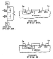
- Figs. 1A and 1B illustrate a simple conventional, junction-isolation, N-well CMOS circuit with its associated PN junction diodes.
- the normally-positive V DD supply pad becomes the negative supply
- the normally-negative V SS supply pad becomes the positive supply.
- the diodes associated with the circuit are forward biased, the current from the battery through the circuit becomes very large and the circuit is destroyed.
- Fig. 2 illustrates the same prior art circuit which is implemented utilizing P-well technology.
- the conventional solution to the reverse battery problem is to provide either a large external resistor or an external diode in series with the V DD supply pad to prevent large currents from flowing through the circuit during reverse battery.
- use of these external devices creates a large voltage drop across the device during normal operation of the circuit.
- the present invention provides a solution to the above-described reverse battery problem by placing a large MOS field effect transistor between the operative circuit and one of the two supply pads of the circuit.
- the gate of the field effect device is connected to the other supply pad.
- the body of the field effect transistor is connected to the source/drain node which is connected to the operative circuit.
- an N-channel device has its drain and source regions connected between the circuit to be protected and the circuit's V SS pad.
- the gate of the N-channel device is connected to the circuit's V DD pad.
- the N-channel device is connected so that, in a forward battery condition, it is turned on as hard as possible by applying the V DD positive supply to its gate.
- the gate of the N-channel device is biased negative and its diodes are off, preventing current flow through the circuit.
- a P-channel device can be similarly utilized by connecting its drain and source regions between the operative circuit and the V DD pad.
- the gate of the P-channel device is connected to the V SS pad.
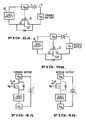
- Fig. 3A shows an operative logic circuit 10 connected between a V DD supply pad and a V SS supply pad. Under normal operating conditions, as illustrated in Fig. 3A, a battery 11 is forward connected so that the V DD pad provides the positive supply and the V SS pad is the negative connection to the circuit 10.
- a protective N-channel field effect transistor 12 has its drain and source regions connected between the operative circuit 10 and the V SS pad, the gate of the N-channel device 12 being connected to the V DD pad.
- the V BS of device 12 is slightly positive to lower its threshold voltage. Thus, as illustrated in Fig. 3A, in a forward battery condition, the positive supply at the V DD pad turns device 12 on as hard as possible so that there is minimal voltage drop across device 12.
- a reverse battery condition i.e. when the the polarity of the battery is reversed so that the V SS pad provides the positive supply, the gate of device 12 is biased negative and the diodes are off. This prevents current from flowing through the logic circuit 10. In this manner, the logic circuit 10 is protected from excessive destructive current in a reverse battery condition.
- the circuit described in conjunction with Figs. 3A and 3B operates much better than placing an integrated diode or resistor in series with the V DD pad, since the forward bias voltage drop of these devices is approximately 0.6V, while the V DS of the transistor 12 can be less than 0.1V.
- the N-channel device 12 is configured in a unique, non-conventional manner with its body connected to its drain in the forward battery condition.
- a P-channel device can also be used to provide reverse battery protection.
- the choice of whether a P-channel or a N-channel reverse battery protection transistor is used depends upon a number of factors: the simultaneous total maximum output sink current and V OH required, the simultaneous total maximum output source current and V OL required, the input voltage level low required, and the input voltage level high relative to V DD required.
- the protective transistor's V DS will make V OL and V IL more difficult to meet if an N-channel device is selected.
- V OH and V IH will be more difficult to meet if a P-channel device is selected.
- an N-channel device will be preferred because the device size required is smaller.
Landscapes
- Charge And Discharge Circuits For Batteries Or The Like (AREA)
- Semiconductor Integrated Circuits (AREA)
- Metal-Oxide And Bipolar Metal-Oxide Semiconductor Integrated Circuits (AREA)
- Protection Of Static Devices (AREA)
Applications Claiming Priority (2)
| Application Number | Priority Date | Filing Date | Title |
|---|---|---|---|
| US9126687A | 1987-08-31 | 1987-08-31 | |
| US91266 | 1987-08-31 |
Publications (2)
| Publication Number | Publication Date |
|---|---|
| EP0305936A2 true EP0305936A2 (fr) | 1989-03-08 |
| EP0305936A3 EP0305936A3 (fr) | 1991-03-27 |
Family
ID=22226893
Family Applications (1)
| Application Number | Title | Priority Date | Filing Date |
|---|---|---|---|
| EP19880114011 Withdrawn EP0305936A3 (fr) | 1987-08-31 | 1988-08-27 | Protection de circuits intégrés MOS contre l'inversion des bornes de la batterie |
Country Status (3)
| Country | Link |
|---|---|
| EP (1) | EP0305936A3 (fr) |
| JP (1) | JPS6472565A (fr) |
| CA (1) | CA1314311C (fr) |
Cited By (4)
| Publication number | Priority date | Publication date | Assignee | Title |
|---|---|---|---|---|
| EP0436778A3 (en) * | 1990-01-11 | 1991-11-13 | Vdo Adolf Schindling Ag | Circuit for the protection of a consumer |
| EP0512605A1 (fr) * | 1991-05-03 | 1992-11-11 | Koninklijke Philips Electronics N.V. | Dispositif de puissance ayant une protection contre des tensions inverses |
| WO1998013922A1 (fr) * | 1996-09-26 | 1998-04-02 | Becton Dickinson And Company | Circuit servant a proteger des circuits electroniques contre une inversion de tension d'entree |
| US6556400B1 (en) * | 1999-08-13 | 2003-04-29 | Micronas Gmbh | Reverse polarity protection circuit |
Families Citing this family (1)
| Publication number | Priority date | Publication date | Assignee | Title |
|---|---|---|---|---|
| EP3101686B1 (fr) * | 2014-01-31 | 2019-04-17 | Alps Alpine Co., Ltd. | Dispositif de circuit intégré à semi-conducteur |
Family Cites Families (1)
| Publication number | Priority date | Publication date | Assignee | Title |
|---|---|---|---|---|
| DE3535788A1 (de) * | 1985-09-03 | 1986-02-20 | Siemens AG, 1000 Berlin und 8000 München | Verpolungsschutz fuer schaltungsanordnungen |
-
1988
- 1988-08-27 EP EP19880114011 patent/EP0305936A3/fr not_active Withdrawn
- 1988-08-30 CA CA000576060A patent/CA1314311C/fr not_active Expired - Fee Related
- 1988-08-31 JP JP63215358A patent/JPS6472565A/ja active Pending
Cited By (4)
| Publication number | Priority date | Publication date | Assignee | Title |
|---|---|---|---|---|
| EP0436778A3 (en) * | 1990-01-11 | 1991-11-13 | Vdo Adolf Schindling Ag | Circuit for the protection of a consumer |
| EP0512605A1 (fr) * | 1991-05-03 | 1992-11-11 | Koninklijke Philips Electronics N.V. | Dispositif de puissance ayant une protection contre des tensions inverses |
| WO1998013922A1 (fr) * | 1996-09-26 | 1998-04-02 | Becton Dickinson And Company | Circuit servant a proteger des circuits electroniques contre une inversion de tension d'entree |
| US6556400B1 (en) * | 1999-08-13 | 2003-04-29 | Micronas Gmbh | Reverse polarity protection circuit |
Also Published As
| Publication number | Publication date |
|---|---|
| EP0305936A3 (fr) | 1991-03-27 |
| JPS6472565A (en) | 1989-03-17 |
| CA1314311C (fr) | 1993-03-09 |
Similar Documents
| Publication | Publication Date | Title |
|---|---|---|
| US4857985A (en) | MOS IC reverse battery protection | |
| US5617283A (en) | Self-referencing modulation circuit for CMOS integrated circuit electrostatic discharge protection clamps | |
| US4789917A (en) | MOS I/O protection using switched body circuit design | |
| US5502328A (en) | Bipolar ESD protection for integrated circuits | |
| US7072157B2 (en) | Electrostatic discharge protection circuit device | |
| US6657835B2 (en) | ESD protection circuit for mixed-voltage I/O by using stacked NMOS transistors with substrate triggering technique | |
| US6927957B1 (en) | Electrostatic discharge clamp | |
| US10298215B2 (en) | Integrated circuit electrostatic discharge protection | |
| US6078487A (en) | Electro-static discharge protection device having a modulated control input terminal | |
| US5708550A (en) | ESD protection for overvoltage friendly input/output circuits | |
| US6577480B1 (en) | Adjustable trigger voltage circuit for sub-micrometer silicon IC ESD protection | |
| JPH11274911A (ja) | 耐電圧性出力バッファ | |
| JP3169537B2 (ja) | 保護回路を有する電気回路及び保護回路に電力供給する方法。 | |
| US7855862B1 (en) | Electrostatic discharge (ESD) circuit and method that includes P-channel device in signal path | |
| US20070103825A1 (en) | High voltage ESD circuit by using low-voltage device with substrate-trigger and gate-driven technique | |
| US4441035A (en) | CMOS Turn-on circuit | |
| KR100334365B1 (ko) | 시모스 입력 버퍼 보호 회로 | |
| US5579200A (en) | Electrostatic discharge protection for metal-oxide-silicon feedback elements between pins | |
| US5705941A (en) | Output driver for use in semiconductor integrated circuit | |
| EP0305936A2 (fr) | Protection de circuits intégrés MOS contre l'inversion des bornes de la batterie | |
| US5963083A (en) | CMOS reference voltage generator | |
| KR19990029708A (ko) | 정전 방전에 대한 보호 회로를 가진 반도체 집적 회로 | |
| JP3499578B2 (ja) | 半導体集積回路 | |
| US8254069B2 (en) | ESD protection for outputs | |
| KR100631961B1 (ko) | 정전기 방전 보호 회로 |
Legal Events
| Date | Code | Title | Description |
|---|---|---|---|
| PUAI | Public reference made under article 153(3) epc to a published international application that has entered the european phase |
Free format text: ORIGINAL CODE: 0009012 |
|
| AK | Designated contracting states |
Kind code of ref document: A2 Designated state(s): DE FR GB IT NL |
|
| PUAL | Search report despatched |
Free format text: ORIGINAL CODE: 0009013 |
|
| AK | Designated contracting states |
Kind code of ref document: A3 Designated state(s): DE FR GB IT NL |
|
| 17P | Request for examination filed |
Effective date: 19910905 |
|
| 17Q | First examination report despatched |
Effective date: 19921229 |
|
| STAA | Information on the status of an ep patent application or granted ep patent |
Free format text: STATUS: THE APPLICATION IS DEEMED TO BE WITHDRAWN |
|
| 18D | Application deemed to be withdrawn |
Effective date: 19930709 |