EP0306002A1 - Procédé d'ajustement adaptatif de phase dans un dispositif d'interconnexion de signaux numériques synchronisés à large bande - Google Patents
Procédé d'ajustement adaptatif de phase dans un dispositif d'interconnexion de signaux numériques synchronisés à large bande Download PDFInfo
- Publication number
- EP0306002A1 EP0306002A1 EP88114209A EP88114209A EP0306002A1 EP 0306002 A1 EP0306002 A1 EP 0306002A1 EP 88114209 A EP88114209 A EP 88114209A EP 88114209 A EP88114209 A EP 88114209A EP 0306002 A1 EP0306002 A1 EP 0306002A1
- Authority
- EP
- European Patent Office
- Prior art keywords
- clock
- test
- digital signal
- signal
- coupling
- Prior art date
- Legal status (The legal status is an assumption and is not a legal conclusion. Google has not performed a legal analysis and makes no representation as to the accuracy of the status listed.)
- Granted
Links
- 238000000034 method Methods 0.000 title claims abstract description 19
- 230000003044 adaptive effect Effects 0.000 title claims description 6
- 230000001360 synchronised effect Effects 0.000 title claims description 5
- 238000012360 testing method Methods 0.000 claims abstract description 90
- 230000008929 regeneration Effects 0.000 claims abstract description 21
- 238000011069 regeneration method Methods 0.000 claims abstract description 21
- 230000008878 coupling Effects 0.000 claims description 90
- 238000010168 coupling process Methods 0.000 claims description 90
- 238000005859 coupling reaction Methods 0.000 claims description 90
- 239000011159 matrix material Substances 0.000 claims description 10
- 230000006978 adaptation Effects 0.000 claims description 8
- 238000004891 communication Methods 0.000 description 3
- 238000012544 monitoring process Methods 0.000 description 3
- 230000005540 biological transmission Effects 0.000 description 2
- 230000002950 deficient Effects 0.000 description 2
- 238000003745 diagnosis Methods 0.000 description 2
- 230000010363 phase shift Effects 0.000 description 2
- 230000002250 progressing effect Effects 0.000 description 2
- 238000005070 sampling Methods 0.000 description 2
- 230000003111 delayed effect Effects 0.000 description 1
- 238000013461 design Methods 0.000 description 1
- 238000011161 development Methods 0.000 description 1
- 230000018109 developmental process Effects 0.000 description 1
- 238000010586 diagram Methods 0.000 description 1
- 238000005516 engineering process Methods 0.000 description 1
- 239000000835 fiber Substances 0.000 description 1
- 230000003287 optical effect Effects 0.000 description 1
- 230000001960 triggered effect Effects 0.000 description 1
Images


Classifications
-
- H—ELECTRICITY
- H04—ELECTRIC COMMUNICATION TECHNIQUE
- H04L—TRANSMISSION OF DIGITAL INFORMATION, e.g. TELEGRAPHIC COMMUNICATION
- H04L7/00—Arrangements for synchronising receiver with transmitter
- H04L7/04—Speed or phase control by synchronisation signals
- H04L7/10—Arrangements for initial synchronisation
-
- H—ELECTRICITY
- H04—ELECTRIC COMMUNICATION TECHNIQUE
- H04J—MULTIPLEX COMMUNICATION
- H04J3/00—Time-division multiplex systems
- H04J3/02—Details
- H04J3/04—Distributors combined with modulators or demodulators
Definitions
- the digital signals are switched through line-coded, so that a line-specific signal regeneration is possible at the output of the coupling arrangement;
- corresponding signal regenerators can also be provided between their coupling stages.
- Synchronous coupling arrangements are operated with a uniform system clock with a clock frequency corresponding to the frequency of the digital signals to be switched, with signal regeneration tion are inserted into the intermediate lines running between the coupling stages and / or into the coupling stages themselves system-clock-controlled bistable flip-flops, to which the system clock is supplied via corresponding delay elements in a phase position that corresponds to the digital signals switched through in the coupling arrangement up to the relevant intermediate line ( DE-C2-2 836 695 Fig. 1 and 2; 1986 Intern. Switzerland Seminar Conference Papers C.4.1 ... 4); the clock phase of the system clock should coincide with the time center of a digital signal element that has just been switched through, so that the signal element in question is regenerated with high reliability.
- the invention relates to a method for adaptive phase adjustment of the system clock signal and digital signal elements switched through in a clock-synchronously operated broadband digital signal coupling arrangement.
- this method is characterized in that that during a connection establishment a test signal fed into the relevant coupling arrangement input is received by a test receiver which is temporarily connected to the output of a coupling stage just reached in the course of the connection establishment and is regenerated to different clock phases, that the clock phases leading to an error-free test signal regeneration are determined as acceptable clock phases, that a clock phase is determined as the optimal clock phase from these acceptable clock phases and is made effective for the further connection duration for the digital signal regeneration at the output of the coupling stage concerned, and that the test receiver is then switched off again, after which these process steps are repeated at the output of each subsequent coupling stage;
- the method according to the invention can also be used in such a way that that during a connection a test signal fed into the relevant coupling arrangement input is repeated - for example
- a central test receiver for a large number of output lines of a coupling stage is sufficient for the recording and regeneration of the test signal at different clock phases;
- Such a central test receiver can therefore also be relatively complex in order to determine an optimal sampling time.
- the system clock signals of different clock phases can also be formed centrally for a coupling stage;
- the clock adaptation devices provided centrally for a multiplicity of output lines of a coupling stage can be integrated in the coupling stage module.
- a coupling field test is also connected to the clock adaptation: If no clock phase is found for which the test signal is correctly regenerated, then the coupling stage just reached proves to be defective due to the clock adaptation progressively progressing from coupling stage to coupling stage.
- the acceptable clock phases can be determined in such a way that the acceptable clock phases are determined by comparing the test signals regenerated to different clock phases with the test signal pattern fed in. The actual comparison of the original test signal pattern and test signals regenerated to different clock phases and the selection of the optimal clock phase can also be carried out by means of a microprocessor, which makes it possible to introduce more complex selection criteria.
- a more precise error diagnosis for example with regard to double connections, can also be made possible by feeding in different test patterns in a further embodiment of the invention.
- any digital signal elements can also be used as a test pattern - then not known on the test receiver side - the test receiver side of several neighboring clock phases, each of which with each other matching regenerated digital signal elements occur, a middle clock phase can be determined as the optimal clock phase. In this case, it is not necessary to feed in a separate test bit pattern, and the useful signal itself can be used for clock adaptation.
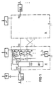
- the coupling arrangement has two coupling stages K1, Kk, via which input lines E, ... can be switched through to output lines A, ....
- the input lines E, ... and output lines A, ... can be, for example, optical waveguides, each of which via an broadband line termination module BLM containing an optoelectric or electro-optical converter to an associated input ek1, ... der first coupling stage (K1) or output kka, ... the last coupling stage (Kk) may be connected.
- the coupling stage inputs ek1, ... lead to corresponding inputs em1, ... of a coupling matrix KM1, whose outputs m1a, ... in turn lead to the outputs k1a, ... of the coupling stage K1 lead.
- each coupling stage is supplied with the system clock at a central clock input T, from which clock signals of the same frequency appear on the coupling stage in a clock phase generator TP (to be implemented, for example, with a tapped delay line (delay chain)) on separate clock signal lines T1, ..., Tn , but with different phases.
- TP clock phase generator
- a digital signal regenerator R is inserted between the coupling matrix outputs m1a, ... and the subsequent coupling stage outputs k1a, ..., in which the digital signal elements that are switched through are regenerated (in terms of time and amplitude); this is expediently done by scanning each switched-through digital signal element with the aid of a bistable flip-flop element controlled by the system clock in a specific phase position, as can be seen in more detail for example from FIG.
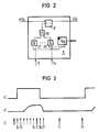
- Such a digital signal regenerator is shown in further circuitry details in FIG.
- the bistable flip-flop (D flip-flop) inserted between the coupling matrix output (m1a) and the coupling stage output (k1a) is designated FF here; to the clock input of the bistable flip-flop FF leads an OR gate Ot, which combines a series of AND gates U1, ..., Un, which in turn from the clock signal lines T1, ..., Tn (see also in FIG 1) system phases are applied to different phases.
- a connection is now made during the establishment of a connection in the switching arrangement input occupied by this connection, for example in the input ek1 of the broadband digital signal switching arrangement outlined in FIG Test signal fed. 1 indicates that a test signal generator PG is provided, which can be connected via the respective broadband line termination module BLM to the associated coupling arrangement input, in the example to input ek1.
- a test signal generator PG is provided, which can be connected via the respective broadband line termination module BLM to the associated coupling arrangement input, in the example to input ek1.
- a test receiver PE1 can be briefly connected to the output of the coupling matrix KM1 reached by the relevant connection, for example to its output m1a, so that this is switched through via the coupling matrix KM1 in the course of the connection that is currently being set up Test signal reaches test receiver PE1.
- a microprocessor ⁇ P may evaluate the agreement between the test signal received and regenerated test signal received by the test receiver PE1 and the test signal pattern fed in at the coupling stage input, the microprocessor ⁇ P making successively different clock phases T1, ..., Tn effective in so far as the test receiver PE1, which is designed as a clock regenerator.
- the clock phases at which the test signal is regenerated in an unadulterated manner are stored in the microprocessor as acceptable clock phases (Ts, Tt, Tn in FIG. 3); From these acceptable clock phases, the microprocessor then selects one, for example the clock phase lying in the middle of the acceptable clock phase, as the optimal clock phase and stores it in the register Reg (in FIG. 2) of the associated digital signal regenerator R, so that during the subsequent one Connection that the AND gate corresponding to the optimal clock phase (U1, ..., Un in FIG 2) is unlocked. This optimal clock phase is thus effective for the further connection duration for the digital signal regeneration at the output k1a of the coupling stage K1.
- the test receiver PE is then switched off again. As can also be seen from FIG.
- the switching on and off of the test receiver PE 1 can be controlled by the microprocessor ⁇ P, which also controls the coupling matrix KM1 of the coupling stage K1; As is further indicated in FIG. 1, the microprocessor .mu.P can in turn be controlled by a higher-level switching controller that is not shown in FIG. 1. In a corresponding manner, the microprocessor of the coupling stage Kk and possibly also the test signal generator PG can be controlled by the higher-level switching control.
- a switching matrix test is also associated with such a clock adaptation: If no clock phase was found in a coupling stage for which the test signal is correctly regenerated, the coupling stage in question proves to be defective because of the clock adaptation progressively progressing from coupling stage to coupling stage.
- a more precise error diagnosis can be made possible by the fact that the test signal generator PG (in FIG. 1) feeds different test signal patterns for each connection, which are simultaneously communicated separately to the respective test recipient; The test receiver can then determine in each case whether the switching stage output in question (only) from the connection belonging to the switching stage output concerned Coupling arrangement input was reached or, for example, in a double connection that was erroneously created (also) by a completely different coupling stage input.
- test generator PG enters the coupling arrangement input of a e.g. Semi-permanent existing connection repeatedly feeds a test signal (e.g.
- the above explanation of an exemplary embodiment of the invention is based on the determination of acceptable clock phases by comparing the test signals regenerated to different clock phases (T1, ..., Tn in FIG. 3) with the test signal pattern fed in, assuming that the test signal pattern as such is available on the test receiver side; This can be achieved, for example, by such a (particularly uniform) test signal pattern being permanently stored on the test receiver side or by the respective (in particular connection-specific) test signal pattern using the associated microprocessor ( ⁇ P in FIG. 1) or the higher-level switching control from case to case the test receiver (PE1 in FIG 1) is supplied.
- test receiver With the appropriate design of the test receiver, it is also possible to dispense with a comparison of the regenerated test signal with the known test signal pattern and to determine the acceptable clock phases directly from a test signal regenerated to different clock phases, which is then also generated by an 0 "or permanent" 1 "different) bit sequence, e.g. can also be formed by any frame synchronous or useful signal word.
- test receiver PE n has clock-controlled bistable flip-flops FF1, ..., FFn for the different clock phases T1, ..., Tn (in FIG. 3 and in FIG. 5), which on the input side from the test receiver input pe have the one to be regenerated Digital signal are applied.
- groups of (for example 3) clock-controlled bistable flip-flops in each case in directly successive clock phases are each combined by an equivalence element, so the bistable flip-flops FFn, FF1 and FF2 by an equivalence element A1, the bistable flip-flops FFs, FFt, FFn by one Equivalence element At and the bistable flip-flops FFt, FFn and FF1 by an equivalence element An.
- the coincidence condition is met if one and the same digital signal element is (re-) generated for the respective successive clock phases;
- the middle clock phase is then the optimal clock phase and can be saved and displayed as such by a bistable flip-flop S1, ...
- FIG. 5 a digital signal eye diagram is shown in FIG. 5, which is sampled at the clock phases shown in line t). The sampling may be based on an (undistorted) digital signal, as shown in line u). Lines ff1), ffs), fft) and ffn) then show the signal states of the bistable flip-flops FF1, FFs, FFt and FFn (in FIG. 4) which result from this scanning; From this illustration it can also be seen that the clock phase Tt proves to be the optimal clock phase under the conditions outlined.
- the digital signal regenerators (R in FIG. 1) each associated with a coupling stage, an associated clock phase regenerator (TP in FIG. 1) and the test receiver (PE1 in FIG. 1) should be on an IC module be integrated, preferably together with the associated coupling matrix (KM1 in FIG. 1) on one and the same IC module, as is also indicated in FIG. 1 with a dash-dotted line.
Landscapes
- Engineering & Computer Science (AREA)
- Computer Networks & Wireless Communication (AREA)
- Signal Processing (AREA)
- Synchronisation In Digital Transmission Systems (AREA)
Priority Applications (1)
| Application Number | Priority Date | Filing Date | Title |
|---|---|---|---|
| AT88114209T ATE75088T1 (de) | 1987-09-01 | 1988-08-31 | Verfahren zur adaptiven phasenanpassung in einer taktsynchron betriebenen breitband-digitalsignal- koppelanordnung. |
Applications Claiming Priority (2)
| Application Number | Priority Date | Filing Date | Title |
|---|---|---|---|
| DE3729171 | 1987-09-01 | ||
| DE3729171 | 1987-09-01 |
Publications (2)
| Publication Number | Publication Date |
|---|---|
| EP0306002A1 true EP0306002A1 (fr) | 1989-03-08 |
| EP0306002B1 EP0306002B1 (fr) | 1992-04-15 |
Family
ID=6334966
Family Applications (1)
| Application Number | Title | Priority Date | Filing Date |
|---|---|---|---|
| EP88114209A Expired - Lifetime EP0306002B1 (fr) | 1987-09-01 | 1988-08-31 | Procédé d'ajustement adaptatif de phase dans un dispositif d'interconnexion de signaux numériques synchronisés à large bande |
Country Status (3)
| Country | Link |
|---|---|
| EP (1) | EP0306002B1 (fr) |
| AT (1) | ATE75088T1 (fr) |
| DE (1) | DE3870104D1 (fr) |
Cited By (1)
| Publication number | Priority date | Publication date | Assignee | Title |
|---|---|---|---|---|
| WO2006127068A1 (fr) * | 2005-05-20 | 2006-11-30 | Honeywell International Inc. | Detecteur de phase de bord de donnees-bord d'horloge pour circuits a grande vitesse |
Citations (3)
| Publication number | Priority date | Publication date | Assignee | Title |
|---|---|---|---|---|
| US3823269A (en) * | 1971-08-11 | 1974-07-09 | Nippon Electric Co | Speech path test system for time-division switching equipment |
| DE2836695A1 (de) * | 1978-08-22 | 1980-03-06 | Siemens Ag | Digitalsignal-vermittlungssystem |
| WO1982004515A1 (fr) * | 1981-06-16 | 1982-12-23 | Beesley Graham Edgar | Dispositif de reglage de synchronisation de bits |
-
1988
- 1988-08-31 DE DE8888114209T patent/DE3870104D1/de not_active Expired - Lifetime
- 1988-08-31 AT AT88114209T patent/ATE75088T1/de active
- 1988-08-31 EP EP88114209A patent/EP0306002B1/fr not_active Expired - Lifetime
Patent Citations (3)
| Publication number | Priority date | Publication date | Assignee | Title |
|---|---|---|---|---|
| US3823269A (en) * | 1971-08-11 | 1974-07-09 | Nippon Electric Co | Speech path test system for time-division switching equipment |
| DE2836695A1 (de) * | 1978-08-22 | 1980-03-06 | Siemens Ag | Digitalsignal-vermittlungssystem |
| WO1982004515A1 (fr) * | 1981-06-16 | 1982-12-23 | Beesley Graham Edgar | Dispositif de reglage de synchronisation de bits |
Non-Patent Citations (2)
| Title |
|---|
| PROCEEDINGS IEEE INTERNATIONAL SYMPOSIUM ON CIRCUITS AND SYSTEMS, San Jose, California, 5.-7. Mai 1986, Band 3, Seiten 1298-1301, IEEE, New York, US; J.P. HEIN: "LSI architectures for data/clock recovery" * |
| PROCEEDINGS OF THE IEEE, Band 65, Nr. 9, September 1977, Seiten 1363-1374, New York, US; S.R. TREVES: "Maintenance strategies for PCM circuit switching" * |
Cited By (2)
| Publication number | Priority date | Publication date | Assignee | Title |
|---|---|---|---|---|
| WO2006127068A1 (fr) * | 2005-05-20 | 2006-11-30 | Honeywell International Inc. | Detecteur de phase de bord de donnees-bord d'horloge pour circuits a grande vitesse |
| US7555089B2 (en) | 2005-05-20 | 2009-06-30 | Honeywell International Inc. | Data edge-to-clock edge phase detector for high speed circuits |
Also Published As
| Publication number | Publication date |
|---|---|
| EP0306002B1 (fr) | 1992-04-15 |
| DE3870104D1 (de) | 1992-05-21 |
| ATE75088T1 (de) | 1992-05-15 |
Similar Documents
| Publication | Publication Date | Title |
|---|---|---|
| DE2848255C2 (fr) | ||
| LU87892A1 (de) | Optisches datennetz hoher betriebssicherheit | |
| DE4017494A1 (de) | Fehlerdetektor fuer eine fernmeldeschaltung | |
| EP0028416A1 (fr) | Système de commutation à large bande | |
| DE2149911C3 (de) | Schaltungsanordnung zur gegenseitigen Synchronisierung der in den Vermittlungsstellen eines PCM-Zeitmultiplexfernmeldenetzes vorgesehenen Amtstaktoszillatoren | |
| EP0363513B1 (fr) | Procedé et dispositif de réception d'un signal numérique binaire | |
| EP0291135B1 (fr) | Etage de concentration pour un système de commutation à large bande | |
| DE69231142T2 (de) | Optisches Vermittlungssystem | |
| WO1987004035A1 (fr) | Systeme permettant le fonctionnement simultane de plusieurs terminaux sur un bloc de raccordement d'un reseau a large bande | |
| EP0306002B1 (fr) | Procédé d'ajustement adaptatif de phase dans un dispositif d'interconnexion de signaux numériques synchronisés à large bande | |
| EP0163288B1 (fr) | Méthode pour tester des chemins commutés d'un réseau de connexion multiplex à division dans l'espace | |
| EP0063638B1 (fr) | Système de télécommunication numérique | |
| DE3608397A1 (de) | System und einrichtung zur seriellen datenuebertragung | |
| EP0301481B1 (fr) | Dispositif de synchronisation pour un démultiplexeur de signaux numériques | |
| EP0645908B1 (fr) | Procédé de multiplexage par partage du temps | |
| EP1061672B1 (fr) | Synchronisation de stations de base dans un système DECT | |
| DE2904076C2 (de) | Adressenfreies Fehlerortungsverfahren für digitale Übertragungssysteme | |
| DE2420437A1 (de) | Verfahren zur datenuebertragung in einem plesiochronen netz | |
| DE3219412C2 (fr) | ||
| DE3590008T1 (de) | Gerät zur Synchronisierung von Impulsketten in einem digitalen Telefonsystem | |
| DE2832856C2 (fr) | ||
| DE2548797C2 (de) | Verfahren zur Pulscodemodulation eines Halbleiterlasers und Anordnung zur Durchführung des Verfahrens | |
| EP0120806A2 (fr) | Circuit sélecteur de canal pour des canaux numériques à large bande à intercalage de bits | |
| DE3116817A1 (de) | Digital-fernmeldesystem | |
| DE3135757A1 (de) | "koppelnetz fuer pcm-kanaele" |
Legal Events
| Date | Code | Title | Description |
|---|---|---|---|
| PUAI | Public reference made under article 153(3) epc to a published international application that has entered the european phase |
Free format text: ORIGINAL CODE: 0009012 |
|
| AK | Designated contracting states |
Kind code of ref document: A1 Designated state(s): AT BE CH DE FR GB IT LI NL SE |
|
| 17P | Request for examination filed |
Effective date: 19890808 |
|
| 17Q | First examination report despatched |
Effective date: 19910919 |
|
| GRAA | (expected) grant |
Free format text: ORIGINAL CODE: 0009210 |
|
| AK | Designated contracting states |
Kind code of ref document: B1 Designated state(s): AT BE CH DE FR GB IT LI NL SE |
|
| REF | Corresponds to: |
Ref document number: 75088 Country of ref document: AT Date of ref document: 19920515 Kind code of ref document: T |
|
| REF | Corresponds to: |
Ref document number: 3870104 Country of ref document: DE Date of ref document: 19920521 |
|
| ET | Fr: translation filed | ||
| ITF | It: translation for a ep patent filed | ||
| GBT | Gb: translation of ep patent filed (gb section 77(6)(a)/1977) | ||
| PLBE | No opposition filed within time limit |
Free format text: ORIGINAL CODE: 0009261 |
|
| STAA | Information on the status of an ep patent application or granted ep patent |
Free format text: STATUS: NO OPPOSITION FILED WITHIN TIME LIMIT |
|
| 26N | No opposition filed | ||
| EAL | Se: european patent in force in sweden |
Ref document number: 88114209.5 |
|
| PGFP | Annual fee paid to national office [announced via postgrant information from national office to epo] |
Ref country code: DE Payment date: 19961022 Year of fee payment: 9 |
|
| PGFP | Annual fee paid to national office [announced via postgrant information from national office to epo] |
Ref country code: CH Payment date: 19961114 Year of fee payment: 9 |
|
| PGFP | Annual fee paid to national office [announced via postgrant information from national office to epo] |
Ref country code: GB Payment date: 19970715 Year of fee payment: 10 |
|
| PGFP | Annual fee paid to national office [announced via postgrant information from national office to epo] |
Ref country code: AT Payment date: 19970723 Year of fee payment: 10 |
|
| PGFP | Annual fee paid to national office [announced via postgrant information from national office to epo] |
Ref country code: SE Payment date: 19970821 Year of fee payment: 10 Ref country code: NL Payment date: 19970821 Year of fee payment: 10 |
|
| PGFP | Annual fee paid to national office [announced via postgrant information from national office to epo] |
Ref country code: BE Payment date: 19970822 Year of fee payment: 10 |
|
| PGFP | Annual fee paid to national office [announced via postgrant information from national office to epo] |
Ref country code: FR Payment date: 19970827 Year of fee payment: 10 |
|
| PG25 | Lapsed in a contracting state [announced via postgrant information from national office to epo] |
Ref country code: LI Free format text: LAPSE BECAUSE OF NON-PAYMENT OF DUE FEES Effective date: 19970831 Ref country code: CH Free format text: LAPSE BECAUSE OF NON-PAYMENT OF DUE FEES Effective date: 19970831 |
|
| REG | Reference to a national code |
Ref country code: CH Ref legal event code: PL |
|
| PG25 | Lapsed in a contracting state [announced via postgrant information from national office to epo] |
Ref country code: DE Free format text: LAPSE BECAUSE OF NON-PAYMENT OF DUE FEES Effective date: 19980501 |
|
| PG25 | Lapsed in a contracting state [announced via postgrant information from national office to epo] |
Ref country code: GB Free format text: LAPSE BECAUSE OF NON-PAYMENT OF DUE FEES Effective date: 19980831 Ref country code: BE Free format text: LAPSE BECAUSE OF NON-PAYMENT OF DUE FEES Effective date: 19980831 Ref country code: AT Free format text: LAPSE BECAUSE OF NON-PAYMENT OF DUE FEES Effective date: 19980831 |
|
| PG25 | Lapsed in a contracting state [announced via postgrant information from national office to epo] |
Ref country code: SE Free format text: LAPSE BECAUSE OF NON-PAYMENT OF DUE FEES Effective date: 19980901 |
|
| BERE | Be: lapsed |
Owner name: SIEMENS A.G. Effective date: 19980831 |
|
| PG25 | Lapsed in a contracting state [announced via postgrant information from national office to epo] |
Ref country code: NL Free format text: LAPSE BECAUSE OF NON-PAYMENT OF DUE FEES Effective date: 19990301 |
|
| GBPC | Gb: european patent ceased through non-payment of renewal fee |
Effective date: 19980831 |
|
| PG25 | Lapsed in a contracting state [announced via postgrant information from national office to epo] |
Ref country code: FR Free format text: LAPSE BECAUSE OF NON-PAYMENT OF DUE FEES Effective date: 19990430 |
|
| NLV4 | Nl: lapsed or anulled due to non-payment of the annual fee |
Effective date: 19990301 |
|
| EUG | Se: european patent has lapsed |
Ref document number: 88114209.5 |
|
| REG | Reference to a national code |
Ref country code: FR Ref legal event code: ST |
|
| PG25 | Lapsed in a contracting state [announced via postgrant information from national office to epo] |
Ref country code: IT Free format text: LAPSE BECAUSE OF NON-PAYMENT OF DUE FEES;WARNING: LAPSES OF ITALIAN PATENTS WITH EFFECTIVE DATE BEFORE 2007 MAY HAVE OCCURRED AT ANY TIME BEFORE 2007. THE CORRECT EFFECTIVE DATE MAY BE DIFFERENT FROM THE ONE RECORDED. Effective date: 20050831 |