EP0306523B1 - System zur ausrichtung und arretierung von lötstiften - Google Patents
System zur ausrichtung und arretierung von lötstiften Download PDFInfo
- Publication number
- EP0306523B1 EP0306523B1 EP88903501A EP88903501A EP0306523B1 EP 0306523 B1 EP0306523 B1 EP 0306523B1 EP 88903501 A EP88903501 A EP 88903501A EP 88903501 A EP88903501 A EP 88903501A EP 0306523 B1 EP0306523 B1 EP 0306523B1
- Authority
- EP
- European Patent Office
- Prior art keywords
- mounting portion
- channel
- region
- channels
- connector assembly
- Prior art date
- Legal status (The legal status is an assumption and is not a legal conclusion. Google has not performed a legal analysis and makes no representation as to the accuracy of the status listed.)
- Expired - Lifetime
Links
- 229910000679 solder Inorganic materials 0.000 title claims abstract description 74
- 230000014759 maintenance of location Effects 0.000 title description 2
- 230000013011 mating Effects 0.000 claims abstract description 24
- 238000003780 insertion Methods 0.000 claims description 19
- 230000037431 insertion Effects 0.000 claims description 19
- 230000007704 transition Effects 0.000 claims description 12
- 125000006850 spacer group Chemical group 0.000 abstract description 21
- 239000004020 conductor Substances 0.000 description 9
- 238000013459 approach Methods 0.000 description 4
- 230000000295 complement effect Effects 0.000 description 3
- 230000006835 compression Effects 0.000 description 2
- 238000007906 compression Methods 0.000 description 2
- 230000004907 flux Effects 0.000 description 1
- 238000004519 manufacturing process Methods 0.000 description 1
- 239000000463 material Substances 0.000 description 1
- 230000002093 peripheral effect Effects 0.000 description 1
- 239000004033 plastic Substances 0.000 description 1
- 238000010008 shearing Methods 0.000 description 1
- 229920001169 thermoplastic Polymers 0.000 description 1
- 239000004416 thermosoftening plastic Substances 0.000 description 1
- 239000012808 vapor phase Substances 0.000 description 1
Images



Classifications
-
- H—ELECTRICITY
- H01—ELECTRIC ELEMENTS
- H01R—ELECTRICALLY-CONDUCTIVE CONNECTIONS; STRUCTURAL ASSOCIATIONS OF A PLURALITY OF MUTUALLY-INSULATED ELECTRICAL CONNECTING ELEMENTS; COUPLING DEVICES; CURRENT COLLECTORS
- H01R12/00—Structural associations of a plurality of mutually-insulated electrical connecting elements, specially adapted for printed circuits, e.g. printed circuit boards [PCB], flat or ribbon cables, or like generally planar structures, e.g. terminal strips, terminal blocks; Coupling devices specially adapted for printed circuits, flat or ribbon cables, or like generally planar structures; Terminals specially adapted for contact with, or insertion into, printed circuits, flat or ribbon cables, or like generally planar structures
- H01R12/50—Fixed connections
- H01R12/51—Fixed connections for rigid printed circuits or like structures
- H01R12/55—Fixed connections for rigid printed circuits or like structures characterised by the terminals
- H01R12/57—Fixed connections for rigid printed circuits or like structures characterised by the terminals surface mounting terminals
-
- H—ELECTRICITY
- H01—ELECTRIC ELEMENTS
- H01R—ELECTRICALLY-CONDUCTIVE CONNECTIONS; STRUCTURAL ASSOCIATIONS OF A PLURALITY OF MUTUALLY-INSULATED ELECTRICAL CONNECTING ELEMENTS; COUPLING DEVICES; CURRENT COLLECTORS
- H01R12/00—Structural associations of a plurality of mutually-insulated electrical connecting elements, specially adapted for printed circuits, e.g. printed circuit boards [PCB], flat or ribbon cables, or like generally planar structures, e.g. terminal strips, terminal blocks; Coupling devices specially adapted for printed circuits, flat or ribbon cables, or like generally planar structures; Terminals specially adapted for contact with, or insertion into, printed circuits, flat or ribbon cables, or like generally planar structures
- H01R12/70—Coupling devices
- H01R12/71—Coupling devices for rigid printing circuits or like structures
- H01R12/712—Coupling devices for rigid printing circuits or like structures co-operating with the surface of the printed circuit or with a coupling device exclusively provided on the surface of the printed circuit
- H01R12/716—Coupling device provided on the PCB
-
- H—ELECTRICITY
- H01—ELECTRIC ELEMENTS
- H01R—ELECTRICALLY-CONDUCTIVE CONNECTIONS; STRUCTURAL ASSOCIATIONS OF A PLURALITY OF MUTUALLY-INSULATED ELECTRICAL CONNECTING ELEMENTS; COUPLING DEVICES; CURRENT COLLECTORS
- H01R12/00—Structural associations of a plurality of mutually-insulated electrical connecting elements, specially adapted for printed circuits, e.g. printed circuit boards [PCB], flat or ribbon cables, or like generally planar structures, e.g. terminal strips, terminal blocks; Coupling devices specially adapted for printed circuits, flat or ribbon cables, or like generally planar structures; Terminals specially adapted for contact with, or insertion into, printed circuits, flat or ribbon cables, or like generally planar structures
- H01R12/70—Coupling devices
- H01R12/71—Coupling devices for rigid printing circuits or like structures
Definitions
- the present invention relates to an electrical connector assembly including a solder post alignment and retention system for right angle mounted connectors.
- Right angle connectors are typically mounted on a printed circuit board.
- a complementary connector mates with the right angle connector in a direction parallel to the printed circuit board.
- Contacts in the right angle connector have a mating portion that is parallel to the printed circuit board and a mounting portion that is in electrical contact with circuits on the printed circuit board, with the mounting portion, typically a solder tail, extending from the mating face of the connector substantially at a right angle to the mating portion of the contact.
- Solder tails typically extend through plated through holes in the printed circuit board and are soldered. The array of printed circuit board through holes have the same pattern and spacing as the solder tails extending from the mating face of the connector.
- U.S. Patent No. 4,210,376 discloses a right angle connector in which conductors adjacent their lower ends are provided with retaining lances. The lances are received in recesses in the sidewalls of the channels to retain the conductors in the channels.
- the channels have extremely narrow entrance portions and enlarged inner ends. The inner ends should be dimensional to accommodate the wire conductors and the narrow entrance portion should have a width such that the conductors must be forced into the channels.
- U.S. Patent No. 3,493,916 discloses a right angle connector having a plurality of terminals which have a rearward end portion extending through either a first series of relatively long slots or a second series of relatively short slots in a rearwardly extending flange portion of the connector.
- U.S. Patent No. 4,491,376 Gladd et al employs a slotted locator plate in which the slots are narrower in width than the solder tails. Each slot is aligned vertically with a contact receiving passage in both rows of contact receiving passages. Each slot has two detents formed by recesses in the otherwise parallel walls of the locator plate slots. The lower row of solder tails is bent about an anvil and forced into the forward detents in the locator plate slots. Subsequently, the upper row of solder tails is bent and forced into the rear detents in the locator plate and forced into the rear detents in the locator plate slots.
- Gladd et al do not teach whether all of the tails of one row are bent simultaneously or whether the tails are bent individually or otherwise. Since the tails are wider than the slots it would be difficult if not impossible to simultaneously bend all tails in a row and insert them in respective locator plate. Furthermore there is no teaching of the cross section of the detents relative to the cross section of the tails.
- U.S. Patent No. 4,225,209 discloses a right angle connector in which conductors are received in spaced apart channels with alternate channels being relatively deep.
- the sidewalls of the channels are provided with depressions or recesses which receive barbs integral with and extending laterally from the side edges of the conductors.
- the intermediate portions of the conductors which extend from apertures to the channels are thus held rigidly by the barbs in the channels and by the conductors received in the apertures.
- US-A-4697864 discloses a right angle connector having three rows of contacts.
- the contacts are inserted into contact receiving passages in the connector housing.
- the contact receiving passes open into channels axially aligned therewith on mandrels with a mandrel associated with each row of contacts.
- the contacts are bent over the mandrels forming a right-angled bend and passed into slots in a contact locating plate beneath the mandrels with the slots in line with the contacts.
- the upper and lower rows of contacts are laterally aligned with each other and with a first contact receiving slot.
- the first slot has two widths with a rib on each wall forming the slot extending into the slot along the length thereof.
- the ribs secure the contact at the desired position by an interference fit.
- the middle row of contacts is aligned with a second contact receiving slot having ribs on each wall which secure contacts positioned therein at the desired position by an interference fit.
- the present invention consists in an electrical connector assembly comprising:- a dielectric housing defining a mating face and a mounting face at right angles thereto, said housing having a plurality of terminal receiving passages extending from the mating face to an opposite rear face a locator plate extending rearwardly from the bottom of the rear face and terminating in a rear edge, said locator plate having first and second profiled channels opening into said rear edge, said locator plate between said first and second channels defining a deflectable beam, a plurality of electrical terminals mounted in the housing, each terminal having a mating portion extending into a terminal receiving passage from said opposite rear face and a mounting portion extending at right angles to the mating portion proximate the mounting face, the mounting portions of the terminals being secured in detents in the channels, the or each first channel comprising a region having a width narrower than a mounting portion adapted to be inserted therein, and a detent adjacent said region in the direction of insertion of the mounting portion, said detent being adapted to receive
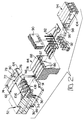
- FIG. 1 there is depicted therein a perspective view of an electrical connector assembly 20 in accordance with the present invention.
- the connector assembly 20 shown is exemplary and is one of a well known type, namely a subminiature D connector of the type manufactured by the applicant, and sold under the trademark AMPLIMITE.
- Connector assembly 20 comprises housing 22 molded of thermoplastic with integral peripheral flange 24, mating face 26, opposed rear face 28 and mounting face 30 at a right angle with respect to mating face 26.
- Cavity 32 is recessed from rear face 28 and defines recessed face 34.
- a plurality of contact receiving passages 36 extend from mating face 26 rearward toward rear face 28, open to recessed face 34 and have contacts 38 secured therein.
- Recessed face 34 is not limited to being planar but could, for example, be stepped.
- Contacts 38 have a mating portion 40 extending into contact receiving passages 36 that may be either pins or sockets and extend into cavity 32 with mounting portions 42, typically solder posts 44, that extend through post spacer plate 46.
- housing 22 is molded in a single piece with post spacer plate 46 integral therewith. Housing 22 also has apertures 48 for removal of vapor phase material. Mating face 26 is surrounded by flange 24 having mounting apertures 50 at opposite ends thereof for securing a complementary connector (not shown) thereto.
- Electrically conductive shell 52 has a similar outer profile to flange 24 with shell mounting apertures 54 aligned with apertures 50. Lugs 56 on the upper portion of shell 52 fold into recesses 58 on flange 24 to secure shell 52 to housing 22. Shroud 60 extends upward from the flat portion of shell 52 and conforms to and encloses the forward raised portion 62 of housing 22.
- Mounting face 30 of connector assembly 20 has integral flanges 64 at opposite ends thereof.
- Each flange 64 has a coplanar mounting face 30 which is received against a printed circuit board (not shown) with channels 66 provided for flux removal, an opposed holding face 68 with aperture 70 extending therebetween.
- Shell 52 has integral ground straps 72 extending to respective mounting faces 30.
- Ground straps 72 fold into channel 74 such that the lower surface of ground strap is coplanar with mounting face 30 and widens near rear face 28 forming shoulders 76 that engage stops 78 to aid in securing ground strap 72 to housing 22 during the unmating of a complementary connector.
- Apertures 80 in the widened region of ground strap 72 align with apertures 70 in flange 64.
- Contacts 38 are formed in a strip on the desired centerline spacing such as in accordance with the teaching of US-A- 4 775 336. During fabrication of a connector assembly 20, contacts 38 on a common carrier strip 82 are unwound from a reel (not shown).
- a length of carrier strip 82 called a "comb" having the number of contacts 38 conforming to the number of contact receiving passages 36 in a row of housing 22 is severed from the reel.
- the solder posts 44 of the contacts 38 on the comb of severed carrier strip 82 are formed to be substantially perpendicular to the mating portion 40 of contacts 38.
- Loading block 84 is inserted into cavity 32 seating on recessed face 34.
- Loading block 84 has a plurality of channels 86 aligned with and corresponding in number to contact receiving passages 36 in a row of passages 36 into which contacts 38 will be inserted. Channels 86 thus provide an extension of contact receiving cavity 36 toward or beyond rear face 28. Channels 86 in loading block 84 open to surface 88 of block 84 through slots 91.
- the row of contact receiving passages 36 closest to post spacer plate 46 is typically the first to receive contacts 38, then the next closest row of contact receiving passages 36 and so on.
- a different loading block 84 is used for each row of passages 36 with channels 86 therein aligned with passages 36.
- Contacts 38, bent 90 degrees and still integral with carrier strip 82 are partially inserted into respective channels 86 in loading block 84.
- Contacts 38 are loose pieced by shearing carrier strip 82 between punch 90 and anvil 92 then inserted to a predetermined depth in passages 36 by passing through respective channels 86 in loading block 84 thence into passages 36.
- Insertion tool 94 provides the insertion force to insert contacts 38 into housing 22.
- mating portion push surface 96 engages the rear surface of mating portion 40
- insertion feature push surface 98 engages insertion feature 100
- solder post push feature 102 engages substantially the length of solder post 44.
- barbs 95 for securing contact 38 in contact receiving passage 38 in an interference fit pass through side channels 87 and solder posts 44 extend through slots 91 and post spacer plate 46. At least portions 104 of insertion tool 94 pass through slot 91 and channels 106 in post spacer plate 46.
- Figure 3 shows a bottom plan view of a post spacer plate 46 broken away from housing 22 for a connector assembly 20 having three rows of contacts 38 and correspondingly three rows of contact receiving passages 36.
- the row of contact receiving passages 36 and contacts 38 closest to post spacer plate 46 is referred to as the lower row.
- the row of contacts receiving passages 36 and contacts 38 most distant from post spacer plate 46 is referred to as the upper row.
- the row of contact receiving passages 36 and contacts 38 between the upper and lower rows is referred to as the middle row.
- Contacts 38 in each row are identical but for the length.
- Post spacer plate 46 is an integral part of housing 22 and extends rearward from contact receiving passages 36 to rear edge 108 which may be flush with rear face 28.
- Post spacer plate 46 has a plurality of channels 112,114 extending forwardly from rear edge 108 and opening thereon. Solder posts 44 from contacts 38 in the upper and lower rows of contact receiving passages 36 pass into and are secured in alternate channels denoted 112. Solder posts from contacts 38 in the middle row of contact receiving passages 36 are secured in alternate channels denoted 114.
- Solder posts 44 from the lower row of contacts 38 are secured in channels 112 first.
- Solder posts 44 have a U-shaped cross section and are inserted into channels 112 with arcuate convex outer surface 116 leading and insertion tool 94 engaging inter alia arcuate concave inner surface 118.
- solder posts 44 engage tapered lead in surfaces 120, the solder post spacer plate 46 between channel 112 and an adjacent channel 114 form beams 122 and 124 that bias or deflect laterally with an effective beam length 126.
- solder posts 44 After passing between tapered lead in surfaces 120, solder posts 44 enter a first region 128 of channel 112 having substantially parallel walls. First region 128 is narrower in width than the uncompressed cross section width of solder posts 44. There is some lateral compression of solder posts 44 in first region 128. Solder posts 44 next enter detent 130 with beams 122 and 124 returning toward their undeflected or unbiased position. Solder posts 44 having a leading arcuate convex outer surface 116 that engages arcuate surfaces 134 in detent 130 again laterally deflects beams 122 and 124 which still have an effective beam length 126 and enters a second region 136 having substantially parallel walls. Second region 136 is narrower in width than the uncompressed cross section width of solder posts 44.
- Solder posts 44 then pass through a first transition region 138 in channel 112, that widens in the direction of insertion of solder posts 44, and into a third region 140 of channel 112 having substantially parallel walls. Third region 140 is narrower in width than the uncompressed cross section width of solder posts 44.
- Solder posts 44 then pass through a second transition region 142, that widens in the direction of insertion of solder posts 44, with channel 112 widening to substantially the width of an uncompressed solder post 44 in fourth region 144.
- Fourth region 144 extends from adjacent the end of channel 114 to neck 146, has substantially parallel walls and provides for free movement of solder posts 44 therealong.
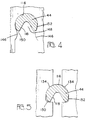
- solder posts 44 then pass through restricting neck 146 to seat in detent 148 as shown in greater detail in Figure 4.
- Detent 148 opens to neck 146, is substantially circular, slightly smaller in diameter than the cross section of an uncompressed solder post 44 and receives solder post 44 in an interference fit. Beams 122 and 124 return to their unbiased position.
- solder posts 44 have a U-shaped cross section having an arcuate convex outer surface 116, an arcuate concave inner surface 118 and planar surfaces 150,152 extending therebetween at two locations. Surfaces 116, 150 and 152 provide an interference fit with detent 148 thereby securing solder posts 44 in detents 148.
- Loading block 84 is removed from cavity 32.
- Solder posts 44 from the middle row of contacts 38 are then secured in channels 114.
- a loading block 84 having channels 86 aligned with contact receiving passages 36 in the middle row is positioned in cavity 32.
- solder posts 44 engage tapered lead in surfaces 120. Beams 122 and 124 deflect laterally with an effective beam length 154 that is the length of channel 114.
- solder posts 44 enter a first region 156 of channel 114 having substantially parallel walls.
- First region 156 is narrower in width than the uncompressed cross section width of solder posts 44 and is substantially the width of third region 140 in channel 112 with beams 122 and 124 undeflected or unbiased.
- Solder posts 44 then pass through a first transition region 158 in channel 114 which narrows in the direction of insertion of solder posts 44. As solder posts 44 pass through first transition region 158, beams 122 and 124 further deflect laterally and solder posts 44 are subjected to further compression.
- Second region 160 has substantially parallel walls and with beams 122 and 124 undeflected is substantially the width of first region 128 and second region 136 in channel 112.
- Detent 162 is formed in the walls of channel 114 as shoulder 164 and arcuate surface 166 which substantially conforms to the curvature of arcuate convex outer surface 116 of solder posts 44.
- Beams 122 and 124 return toward their unbiased position. Since the uncompressed cross section width of solder posts 44 exceeds the width of detent 162 with beams 122 and 124 in an undeflected position, solder posts 44 are secured in detents 162 in an interference fit. Furthermore, beams 122 and 124 remain in a deflected position as illustrated in Figure 6. Loading block is removed from cavity 32.
- Channel 114 extends beyond detent 162 in extension 168 which is too narrow for entry of solder posts 44 and provides beams 122 and 124 with effective lengths greater than the depth of detent 162 during insertion of solder posts 44 in channels 114.
- Solder posts 44 from the top row of contacts 38 are then secured in channel 112.
- a loading block 84 having channels 86 aligned with contact receiving passages 36 in the top row is positioned in cavity 32.
- solder posts 44 engage tapered lead in surfaces 120. Beams 122 and 124 deflect laterally with an effective beam length 170. After passing between tapered lead in surfaces 120 and through first region 128 of channel 112, solder posts 44 seat in detents 130. Detents 130 are shaped like and secure solder posts 44 in the same way as detents 162. Loading block 84 is removed from cavity 32 as insertion of contacts 38 is complete.
Landscapes
- Coupling Device And Connection With Printed Circuit (AREA)
- Multi-Conductor Connections (AREA)
- Connector Housings Or Holding Contact Members (AREA)
Claims (9)
- Elektrische Verbinder - Anordnung (20) mit
einem nichtleitenden Gehäuse (22), das eine Paßfläche (26) festlegt sowie eine Montagefläche (30) rechtwinklig dazu, wobei das Gehäuse (22) eine Vielzahl von Anschlußaufnahmedurchgängen (36) aufweist, die von der Paßfläche (26) zu einer entgegengesetzten rückseitigen Fläche (34) verlaufen,
einer Lokalisierplatte (46), die rückwärts gerichtet verläuft vom Grund der rückseitigen Fläche (34) und endet in einer rückwärtigen Kante (108), wobei die Lokalisierplatte (46) erste und zweite profilierte Kanäle (114, 112) aufweist, die sich in der rückwärtigen Kante (108) öffnen, wobei die Lokalisierplatte (46) zwischen den ersten und zweiten Kanälen einen biegbaren Balken (122, 124) festlegt,
einer Vielzahl elektrischer Anschlüsse (38), die in dem Gehäuse montiert sind, wobei jeder Anschluß einen Paßabschnitt (40) hat, der sich in einen Anschlußaufnahmedurchgang (36) von der entgegengesetzten rückseitigen Fläche (34) her erstreckt, sowie einen Montageabschnitt (42), der rechtwinklig zu dem Paßabschnitt nahe der Montagefläche (30) verläuft, wobei die Montageabschnitte (42) der Anschlüsse (38) in Sperren (130, 148, 162) in den Kanälen (112, 114) gesichert sind,
wobei der oder jeder erste Kanal (114) einen Bereich (156), der eine Breite enger als ein darin einzuführender Montageabschnitt (42) hat, und eine in der Einführrichtung des Montageabschnitts an diesen Bereich angrenzende Sperre (162) aufweist, wobei die Sperre (162) zur Aufnahme des Montageabschnitts von diesem Bereich angepaßt ist, und
wobei der oder jeder zweite Kanal (112), in der Einführrichtung eines Montageabschnitts (42), einen ersten Bereich (140), der eine Breite enger als ein darin einzuführender Montageabschnitt hat, einen Übergangsbereich (142), der an diesen ersten Bereich angrenzt, wobei sich der Übergangsbereich (142) in Einführrichtung des Montageabschnitts zu im wesentlichen der Breite des Montageabschnitts nahe dem Ende des ersten Kanals aufweitet, einen zweiten Bereich (144), der an den Übergangsbereich (142) angrenzt, wobei der zweite Bereich im wesentlichen von der Breite des Montageabschnitts ist, einen Einengungshals (146), der an den Zweiten Bereich angrenzt, und eine Sperre (148) an dem Ende des zweiten Kanals (112) aufweist, wobei die Sperre (148) zum Aufnehmen und Sichern des Montageabschnitts darin angepaßt ist,
wodurch, wenn ein Montageabschnitt (42) in den Bereich (156) des ersten Kanals (114) eingeführt wird, der Balken (122, 124) sich zum zweiten Kanal hin biegt und, wenn ein Montageabschnitt (42) in den ersten Bereich (140) des zweiten Kanals (112) eingeführt wird, der Balken (122, 124) sich zum ersten Kanal (114) hin biegt und, wenn der Montageabschnitt durch den Übergangsbereich (142) geführt wird, der Balken (122, 124) in eine nicht gebogene Stellung zurückkehrt, wobei der Balken (122, 124) in einer nicht gebogenen Stellung verbleibt, wenn der Montageabschnitt durch den zweiten Bereich (144) geführt wird. - Elektrische Verbinder - Anordnung (20) nach Anspruch 1, in der der Montageabschnitt (42) jedes Anschlusses (38) eine Lötfahne ist.
- Elektrische Verbinder - Anordnung (20) nach Anspruch 1 oder 2, in der der Montageabschnitt (42) jedes Anschlusses (38) in einer Sperre (130, 148, 162) in einem Kanal (112, 114) in einem Preßsitz gesichert ist.
- Elektrische Verbinder - Anordnung (20) nach Anspruch 1, 2 oder 3, in der der Montageabschnitt (42) jedes Anschlusses (38) in einer Sperre (130, 148, 162) in einem Kanal (112, 114) gesichert ist, der seitlich mit dem Anschlußaufnahmedurchgang (36) ausgerichtet ist, in den der entsprechende Paßabschnitt (40) verläuft.
- Elektrische Verbinder - Anordnung (20) nach einem der vorhergehenden Ansprüche, in der der erste Kanal (114) sich über die Sperre (162) hinaus erstreckt (168), wobei er darin eine Breite schmaler als der in den ersten Kanal (114) einzuführende Montageabschnitt aufweist.
- Elektrische Verbinder - Anordnung (20) nach einem der vorhergehenden Ansprüche, in der die ersten und zweiten Kanäle (114, 112) schräg zulaufende Einführflächen (120) von der rückwärtigen Kante (108) aufweisen.
- Elektrische Verbinder - Anordnung (20) nach einem der vorhergehenden Ansprüche, in der die Lokalisierplatte (46) ein integraler Bestandteil des Gehäuses (22) ist.
- Elektrische Verbinder - Anordnung (20) nach einem der vorhergehenden Ansprüche, in der die Anzahl der Sperren (130, 148, 162) längs jedes Kanals (112, 114) der Anzahl der zugeordneten Anschlußaufnahmedurchgänge (36) entspricht.
- Elektrische Verbinder - Anordnung (20) nach einem der vorhergehenden Ansprüche, in der jeder Kanal (112, 114) seitlich mit einem oder mehreren Anschlußaufnahmedurchgängen (36) ausgerichtet ist.
Applications Claiming Priority (2)
| Application Number | Priority Date | Filing Date | Title |
|---|---|---|---|
| US31483 | 1987-03-27 | ||
| US07/031,483 US4789346A (en) | 1987-03-27 | 1987-03-27 | Solder post alignment and retention system |
Publications (2)
| Publication Number | Publication Date |
|---|---|
| EP0306523A1 EP0306523A1 (de) | 1989-03-15 |
| EP0306523B1 true EP0306523B1 (de) | 1993-06-16 |
Family
ID=21859706
Family Applications (1)
| Application Number | Title | Priority Date | Filing Date |
|---|---|---|---|
| EP88903501A Expired - Lifetime EP0306523B1 (de) | 1987-03-27 | 1988-03-04 | System zur ausrichtung und arretierung von lötstiften |
Country Status (6)
| Country | Link |
|---|---|
| US (1) | US4789346A (de) |
| EP (1) | EP0306523B1 (de) |
| JP (1) | JP2627948B2 (de) |
| KR (1) | KR970001616B1 (de) |
| DE (1) | DE3881796T2 (de) |
| WO (1) | WO1988007776A1 (de) |
Families Citing this family (32)
| Publication number | Priority date | Publication date | Assignee | Title |
|---|---|---|---|---|
| ES2043705T3 (es) * | 1988-03-26 | 1994-01-01 | Weidmueller Interface | Conector electrico enchufable. |
| US4908335A (en) * | 1988-06-03 | 1990-03-13 | Amp Incorporated | One-piece molded insulating housing for a circular din connector |
| US4915652A (en) * | 1989-06-12 | 1990-04-10 | Thomas & Betts Corporation | Shielded electrical connector |
| US5032085A (en) * | 1990-02-26 | 1991-07-16 | Gte Products Corp. | Electrical connector, and housing and contacts therefor |
| US5080596A (en) * | 1990-11-30 | 1992-01-14 | Amp Incorporated | Connector with contact spacer plate providing greater lateral force on rear contacts |
| US5037334A (en) * | 1990-11-30 | 1991-08-06 | Amp Corporated | Connector with equal lateral force contact spacer plate |
| JP2816435B2 (ja) * | 1990-11-30 | 1998-10-27 | アンプ インコーポレイテッド | コンタクトスペーサ付き電気コネクタ |
| US5071372A (en) * | 1990-11-30 | 1991-12-10 | Amp Incorporated | Connector with contact spacer plate having tapered channels |
| JP2535258Y2 (ja) * | 1991-04-30 | 1997-05-07 | 日本航空電子工業株式会社 | コネクタの係止構造 |
| US5112233A (en) * | 1991-05-30 | 1992-05-12 | Thomas & Betts Corporation | Electrical connector having contact retention means |
| FR2689693B1 (fr) * | 1992-04-03 | 1994-07-08 | Souriau & Cie | Procede d'assemblage d'un connecteur presentant des elements de contacts coudes. |
| EP0735619A1 (de) * | 1995-03-30 | 1996-10-02 | Thomas & Betts Corporation | Elektrischer Verbinder mit verbesserter Kontaktbefestigungsanordnung |
| DE19607548C2 (de) * | 1996-02-28 | 1998-02-26 | Siemens Ag | Abgewinkelter Einpreß-Steckverbinder zum Einpressen in Bohrungen einer Leiterplatte |
| TW340680U (en) * | 1997-05-16 | 1998-09-11 | Molex Taiwan Co Ltd | Lead fastener for electric adapters |
| US5947769A (en) * | 1997-06-03 | 1999-09-07 | Molex Incorporated | Shielded electrical connector |
| BE1011543A3 (nl) * | 1997-11-12 | 1999-10-05 | Framatome Connectors Belgium | Inrichting en werkwijze voor het verwijderen van een connector uit een paneel met gedrukte schakelingen. |
| US6294766B1 (en) * | 1999-07-31 | 2001-09-25 | Microsemi Corporation | Battery cell bypass with pre-loaded compression action |
| US6645006B1 (en) * | 2000-07-05 | 2003-11-11 | Mannesmann Vdo Ag | Electrical connector |
| TW562308U (en) * | 2003-04-02 | 2003-11-11 | Hon Hai Prec Ind Co Ltd | Contact of electrical connector |
| US8735734B2 (en) * | 2009-07-23 | 2014-05-27 | Lexmark International, Inc. | Z-directed delay line components for printed circuit boards |
| US8198547B2 (en) | 2009-07-23 | 2012-06-12 | Lexmark International, Inc. | Z-directed pass-through components for printed circuit boards |
| US8752280B2 (en) | 2011-09-30 | 2014-06-17 | Lexmark International, Inc. | Extrusion process for manufacturing a Z-directed component for a printed circuit board |
| US9009954B2 (en) | 2011-08-31 | 2015-04-21 | Lexmark International, Inc. | Process for manufacturing a Z-directed component for a printed circuit board using a sacrificial constraining material |
| US8943684B2 (en) * | 2011-08-31 | 2015-02-03 | Lexmark International, Inc. | Continuous extrusion process for manufacturing a Z-directed component for a printed circuit board |
| US9078374B2 (en) | 2011-08-31 | 2015-07-07 | Lexmark International, Inc. | Screening process for manufacturing a Z-directed component for a printed circuit board |
| US8790520B2 (en) | 2011-08-31 | 2014-07-29 | Lexmark International, Inc. | Die press process for manufacturing a Z-directed component for a printed circuit board |
| US8658245B2 (en) | 2011-08-31 | 2014-02-25 | Lexmark International, Inc. | Spin coat process for manufacturing a Z-directed component for a printed circuit board |
| US8830692B2 (en) | 2012-03-29 | 2014-09-09 | Lexmark International, Inc. | Ball grid array systems for surface mounting an integrated circuit using a Z-directed printed circuit board component |
| US8822838B2 (en) | 2012-03-29 | 2014-09-02 | Lexmark International, Inc. | Z-directed printed circuit board components having conductive channels for reducing radiated emissions |
| US8912452B2 (en) | 2012-03-29 | 2014-12-16 | Lexmark International, Inc. | Z-directed printed circuit board components having different dielectric regions |
| US8822840B2 (en) | 2012-03-29 | 2014-09-02 | Lexmark International, Inc. | Z-directed printed circuit board components having conductive channels for controlling transmission line impedance |
| JP6744370B2 (ja) | 2018-08-10 | 2020-08-19 | 矢崎総業株式会社 | 基板実装型コネクタ |
Family Cites Families (16)
| Publication number | Priority date | Publication date | Assignee | Title |
|---|---|---|---|---|
| US3025488A (en) * | 1958-10-16 | 1962-03-13 | Bendix Corp | Contact mounting |
| US3493916A (en) * | 1967-07-24 | 1970-02-03 | Molex Products Co | Printed circuit board terminal and connector |
| US3551877A (en) * | 1968-11-20 | 1970-12-29 | Hugh H Eby Co | Electrical connector |
| US3601762A (en) * | 1969-08-15 | 1971-08-24 | Vernitron Corp | Electrical connector |
| US3905673A (en) * | 1972-12-11 | 1975-09-16 | Du Pont | Header block |
| US3864000A (en) * | 1973-06-07 | 1975-02-04 | Amp Inc | Mating contact connector housing assembly |
| US4080041A (en) * | 1977-03-14 | 1978-03-21 | International Telephone And Telegraph Corporation | Electrical connector |
| US4210376A (en) * | 1978-12-07 | 1980-07-01 | Amp Incorporated | Electrical connector receptacle |
| US4186988A (en) * | 1978-09-20 | 1980-02-05 | Amp Incorporated | Electrical connector receptacles |
| US4225209A (en) * | 1979-05-18 | 1980-09-30 | Amp Incorporated | Electrical connector receptacle |
| US4410230A (en) * | 1981-09-02 | 1983-10-18 | Holmberg Electronics Corporation | Connector block |
| JPS5916150A (ja) * | 1982-07-19 | 1984-01-27 | Matsushita Electric Ind Co Ltd | 光記録装置 |
| US4491376A (en) * | 1982-09-20 | 1985-01-01 | General Motors Corporation | Electrical header assembly |
| DE3402902A1 (de) * | 1984-01-27 | 1985-08-08 | Siemens AG, 1000 Berlin und 8000 München | Winkelsteckverbinder |
| JPS6142887A (ja) * | 1984-07-31 | 1986-03-01 | アンプ インコ−ポレ−テツド | 電気コネクタ |
| US4655518A (en) * | 1984-08-17 | 1987-04-07 | Teradyne, Inc. | Backplane connector |
-
1987
- 1987-03-27 US US07/031,483 patent/US4789346A/en not_active Expired - Lifetime
-
1988
- 1988-03-04 KR KR1019880701546A patent/KR970001616B1/ko not_active Expired - Fee Related
- 1988-03-04 JP JP63503145A patent/JP2627948B2/ja not_active Expired - Lifetime
- 1988-03-04 DE DE88903501T patent/DE3881796T2/de not_active Expired - Lifetime
- 1988-03-04 WO PCT/US1988/000620 patent/WO1988007776A1/en not_active Ceased
- 1988-03-04 EP EP88903501A patent/EP0306523B1/de not_active Expired - Lifetime
Also Published As
| Publication number | Publication date |
|---|---|
| JP2627948B2 (ja) | 1997-07-09 |
| WO1988007776A1 (en) | 1988-10-06 |
| JPH01503095A (ja) | 1989-10-19 |
| KR890700944A (ko) | 1989-04-28 |
| EP0306523A1 (de) | 1989-03-15 |
| DE3881796T2 (de) | 1994-01-13 |
| US4789346A (en) | 1988-12-06 |
| DE3881796D1 (de) | 1993-07-22 |
| KR970001616B1 (ko) | 1997-02-11 |
Similar Documents
| Publication | Publication Date | Title |
|---|---|---|
| EP0306523B1 (de) | System zur ausrichtung und arretierung von lötstiften | |
| EP0337659B1 (de) | Lötstift-Rückhaltevorrichtung | |
| EP0488298B1 (de) | Verbinder mit Kontaktdistanzierplatte mit gleichförmiger seitlicher Kraft | |
| US4255009A (en) | Two row electrical connector | |
| US6769935B2 (en) | Matrix connector | |
| JP2855197B2 (ja) | 電気コネクタ | |
| US5080596A (en) | Connector with contact spacer plate providing greater lateral force on rear contacts | |
| EP0555963B1 (de) | Stecker mit einteiligem Massestreifen | |
| US6764349B2 (en) | Matrix connector with integrated power contacts | |
| CA1310085C (en) | High density ribbon cable connector and dual transition contact therefor | |
| US5161996A (en) | Header assembly and alignment assist shroud therefor | |
| US6368148B1 (en) | Ribbon cable connector with ground bus | |
| EP0390450A1 (de) | Stapelbarer Zwillingsverbinder für Schnittstellenbus | |
| US6739918B2 (en) | Self-aligning electrical connector | |
| JP3647951B2 (ja) | 一対の嵌合コンタクトおよび電気コネクタ組立体 | |
| US5100342A (en) | High density flat cable connector | |
| EP0365179B1 (de) | Elektrisches Verbindersystem | |
| EP0740372B1 (de) | Elektrischer Verbinder | |
| EP0487866B1 (de) | Elektrische Verbinderanordung zum Montieren auf gedruckter Leiterplatte | |
| EP0191539B1 (de) | Elektrisches Anschlussendstück für Steckverbinder | |
| EP0775374B1 (de) | Steckverbinder für ein elektrisches kabel | |
| EP0488349B1 (de) | Verbinder mit Kontaktabstandsplatte mit keilförmigen Kanälen | |
| US5308258A (en) | Planar modular interconnect system | |
| US5190483A (en) | Contact retention | |
| EP0205458B2 (de) | Steckverbinder für bandkabel |
Legal Events
| Date | Code | Title | Description |
|---|---|---|---|
| PUAI | Public reference made under article 153(3) epc to a published international application that has entered the european phase |
Free format text: ORIGINAL CODE: 0009012 |
|
| AK | Designated contracting states |
Kind code of ref document: A1 Designated state(s): BE DE FR GB IT NL |
|
| 17P | Request for examination filed |
Effective date: 19881112 |
|
| RAP1 | Party data changed (applicant data changed or rights of an application transferred) |
Owner name: AMP INCORPORATED |
|
| 17Q | First examination report despatched |
Effective date: 19920518 |
|
| RAP1 | Party data changed (applicant data changed or rights of an application transferred) |
Owner name: THE WHITAKER CORPORATION |
|
| RBV | Designated contracting states (corrected) |
Designated state(s): DE FR GB IT NL |
|
| GRAA | (expected) grant |
Free format text: ORIGINAL CODE: 0009210 |
|
| ITF | It: translation for a ep patent filed | ||
| AK | Designated contracting states |
Kind code of ref document: B1 Designated state(s): DE FR GB IT NL |
|
| REF | Corresponds to: |
Ref document number: 3881796 Country of ref document: DE Date of ref document: 19930722 |
|
| ET | Fr: translation filed | ||
| PLBE | No opposition filed within time limit |
Free format text: ORIGINAL CODE: 0009261 |
|
| STAA | Information on the status of an ep patent application or granted ep patent |
Free format text: STATUS: NO OPPOSITION FILED WITHIN TIME LIMIT |
|
| 26N | No opposition filed | ||
| PGFP | Annual fee paid to national office [announced via postgrant information from national office to epo] |
Ref country code: NL Payment date: 19981222 Year of fee payment: 12 |
|
| PG25 | Lapsed in a contracting state [announced via postgrant information from national office to epo] |
Ref country code: NL Free format text: LAPSE BECAUSE OF NON-PAYMENT OF DUE FEES Effective date: 20001001 |
|
| NLV4 | Nl: lapsed or anulled due to non-payment of the annual fee |
Effective date: 20001001 |
|
| REG | Reference to a national code |
Ref country code: GB Ref legal event code: IF02 |
|
| PG25 | Lapsed in a contracting state [announced via postgrant information from national office to epo] |
Ref country code: IT Free format text: LAPSE BECAUSE OF NON-PAYMENT OF DUE FEES Effective date: 20050304 |
|
| PGFP | Annual fee paid to national office [announced via postgrant information from national office to epo] |
Ref country code: GB Payment date: 20070327 Year of fee payment: 20 |
|
| PGFP | Annual fee paid to national office [announced via postgrant information from national office to epo] |
Ref country code: DE Payment date: 20070430 Year of fee payment: 20 |
|
| REG | Reference to a national code |
Ref country code: GB Ref legal event code: PE20 |
|
| PGFP | Annual fee paid to national office [announced via postgrant information from national office to epo] |
Ref country code: FR Payment date: 20070319 Year of fee payment: 20 |
|
| PG25 | Lapsed in a contracting state [announced via postgrant information from national office to epo] |
Ref country code: GB Free format text: LAPSE BECAUSE OF EXPIRATION OF PROTECTION Effective date: 20080303 |