EP0306535B1 - Prozessor für programmierbaren logischen regler und programmierbarer logischer regler - Google Patents
Prozessor für programmierbaren logischen regler und programmierbarer logischer regler Download PDFInfo
- Publication number
- EP0306535B1 EP0306535B1 EP19880901928 EP88901928A EP0306535B1 EP 0306535 B1 EP0306535 B1 EP 0306535B1 EP 19880901928 EP19880901928 EP 19880901928 EP 88901928 A EP88901928 A EP 88901928A EP 0306535 B1 EP0306535 B1 EP 0306535B1
- Authority
- EP
- European Patent Office
- Prior art keywords
- jump
- logic
- processor
- instruction
- plc
- Prior art date
- Legal status (The legal status is an assumption and is not a legal conclusion. Google has not performed a legal analysis and makes no representation as to the accuracy of the status listed.)
- Expired - Lifetime
Links
Images


Classifications
-
- G—PHYSICS
- G05—CONTROLLING; REGULATING
- G05B—CONTROL OR REGULATING SYSTEMS IN GENERAL; FUNCTIONAL ELEMENTS OF SUCH SYSTEMS; MONITORING OR TESTING ARRANGEMENTS FOR SUCH SYSTEMS OR ELEMENTS
- G05B19/00—Program-control systems
- G05B19/02—Program-control systems electric
- G05B19/04—Program control other than numerical control, i.e. in sequence controllers or logic controllers
- G05B19/05—Programmable logic controllers, e.g. simulating logic interconnections of signals according to ladder diagrams or function charts
-
- G—PHYSICS
- G05—CONTROLLING; REGULATING
- G05B—CONTROL OR REGULATING SYSTEMS IN GENERAL; FUNCTIONAL ELEMENTS OF SUCH SYSTEMS; MONITORING OR TESTING ARRANGEMENTS FOR SUCH SYSTEMS OR ELEMENTS
- G05B2219/00—Program-control systems
- G05B2219/10—Plc systems
- G05B2219/13—Plc programming
- G05B2219/13083—Jumps
Definitions
- a PLC programmable logic controller
- PC programmable controller
- FIG. 6 An example of a ladder diagram is shown in Fig. 6, in which numeral 60 indicates a ladder diagram sheet.
- Logic relay contacts are denoted by characters A, B, C, D, E, F, G and H.
- Numeral 61 denotes a coil of the logic relay.
- Such a ladder diagram implements logic processing as indicated below.
- RD A (1) AND ⁇ NOT B (2) AND C (3) AND ⁇ NOT D (4) AND E (S) OR F (6) OR ⁇ NOT G (7) AND H (8) WRT Y (9)
- a processing period can be shortened by omitting some operations which are unnecessary under a prescribed situation and jumping to an operation to be executed. Yet, there is a possibility that in commonly used processors, the processing period might be prolonged when executing check instructions and thus the processing period may not be shortened in all cases.
- FR-A-2268303 over which the present invention is characterised, discloses a PLC processor with jump condition checking.
- a PLC (programmable logic controller) processor for carrying out logic operations, comprising: a logic operation means for executing a logic operation; a jump condition checking means for checking whether or not a logic operation subsequent to a current logic operation should be executed based on a relation between a resultant value of the current logic operation and the kinds of logic operations commanded by the immediately following instructions; characterised by: a jump inhibition means for determining in relation to a particular operation whether a jump may be performed or must be inhibited; and a jump execution means for executing the logic operation subsequent to logic operations for which the jump inhibition means determines that a jump may be performed, only if the jump condition checking means determines that the logic operation should be executed.
- a jump inhibition means for determining in relation to a particular operation whether a jump may be performed or must be inhibited
- a jump execution means for executing the logic operation subsequent to logic operations for which the jump inhibition means determines that a jump may be performed, only if the jump condition checking means determines that the logic operation should be executed.
- the subsequent OR instructions can be omitted.
- the subsequent AND instructions can be omitted.
- the processor of the type as referred to above is exclusively used for executing the logic processes and another processor is employed for executing the remaining processes, whereby the processing period of time can further be reduced.
- Fig. 1 is a block diagram showing a processor according to one embodiment of the invention.
- a processor 1 is comprised of a logic operation means 2, a jump inhibition means 3, a jump condition checking means 4 and a jump execution means 5.
- the logic operation means 2 implements logic operations and executes logic operations of AND, OR, NOT, etc. Other than the logic operation, the logic operation means 2 is capable of executing numerical computations.
- the jump inhibition means 3 check whether or not jump is allowed. For example, a write instruction for writing the result of the logic operation (which corresponds to the instruction Y shown in Fig. 6 and to the instruction (9) set forth in the Background Art section) cannot be omitted, therefore, the instruction preceding such unomittable instruction is inhibited from being jumped. This is accomplished by imposing a jump inhibition to the instruction preceding to the write instruction when the PLC program is assembled or compiled.
- AND-interrelated instructions are omitted, and jump is performed over to OR-interrelated instructions or the write instruction.
- What is referred to by the AND-interrelated instructions is intended to cover not only an AND instruction but also a NOT AND instruction (which instruction corresponds to the logic relay B shown in Fig. 6).
- the jump execution means 5 executes a logic instruction in accordance with conditions supplied from both the jump inhibition means 3 and the jump condition checking means 4. Of course, only when the above-mentioned two conditions are complied with at the same time, the logic instruction is executed. If the conditions are not complied with, the processing immediately advances to the subsequent instruction. A number to be jumped is stored in an external memory 6.
- the memory 6 stores a number of logic instructions and such a number is stored therein in the form of an integer.
- the theory as set forth with respect to the jump condition checking means is equally applied to this number. Specifically, in the case where the AND-interrelated instructions follow, that number is a number of AND-interrelated instructions disposed ahead of the subsequent OR-interrelated or write instructions. On the other hand, in the case of OR-interrelated instructions, that number is a number of the OR-interrelated instructions disposed ahead of the subsequent AND-interrelated or write instructions.
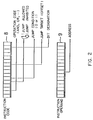
- FIG. 2 there is shown an instruction format of a processor according to this embodiment.
- An instruction is composed of two words.
- Denoted by numeral 8 is a high - order one word providing an instruction code.
- Denoted by numeral 9 is a low-order one word providing an instruction operand.
- the instruction code 8 is provided with functions as shown in the figure.
- the left four bits are a processing code, which, for example, determines instructions, such as AND, OR, etc.
- next one bit it is discriminated whether or not jump is allowed, in which when "1", jump is allowed according to a condition whereas when "0", jump is inhibited.
- the latter corresponds to such instructions that cannot be omitted as in the case of a read instruction (corresponding to the instruction A in Fig. 6) and a write instruction (corresponding to Y in Fig. 6).
- that bit is rendered “0” to inhibit jumping. "1” or "0” of this bit is determined when a source program is converted to an object program.
- the succeeding one bit is for determining a jump condition, which is rendered “1" when the AND-interrelated instructions follow and is rendered "0" when the OR-interrelated instructions follow.
- this bit value is Q said result of a logic operation is S
- P Q ⁇ S ⁇ + Q ⁇ ⁇ S
- the succeeding seven bits are representative of a number of instructions to be jumped.
- this number is equal to the number of such AND-interrelated instructions
- the OR-interrelated instructions follow this number is equal to the number of such OR-interrelated instructions.
- Such numbers are determined when the source program is converted to the object program upon counting a number of instructions.
- the last four bits are representative of bits corresponding to data to be processed.
- data is composed of 16 bits per one word.
- the logic relay which is subjected to logic operation is represented by one-bit data which is specified by using these four bits.
- the word organization and the number of bits can arbitrarily be designed and altered, and variety of word organizations and bit allocations may be made.
- FIG. 3 there is shown a hardware arrangement of the processor according to the present invention.
- Numerals indicated alongside signal lines with an oblique line segment represent a number of bits selected from a bus line for usage.
- numeral 4 represents that four bits are used among the bus line.
- an operation sequence control circuit 21 performs timing controls for the entire processor.
- An instruction operand latch 27 latches the content of the instruction operand 9 (Fig. 2) and outputs it to the multiplexer 29 for fetching a corresponding address.
- An address generation circuit 40 controls addresses for performing jumping based on a relation between the logic operation processes described previously and the subsequent instruction. Details of this address generation will be described later.
- Multiplexers 29 and 30 select buses in response to a timing signal fed from the operation sequence control circuit 21.
- Denoted by numerals 31 and 32 are an address bus drive circuit and a data bus drive circuit, respectively
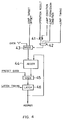
- the address generation circuit is shown in Fig. 4.
- an exclusive-OR circuit (hereinafter referred to as EOR circuit) 41 has one input terminal to which a logic operation result of the execution instruction is applied.
- the EOR circuit 41 has the other input terminal to which the jump condition signal is applied.
- this jump condition signal is "1" in the case where the AND-interrelated instructions follow whereas the signal is "0” in the case where the OR-interrelated instructions follow.
- a multiplexer 43 selects data "1" when the output of the AND circuit 42 is "0", in the case of which the address is counted up one by one.
- a jump target offset (the number of instructions for jumping) is selected.
- An adder 44 adds one to the address of the last instruction when the jump is not performed.
- the jump target offset is selected by the multiplexer 43 and the number of jumps are added to the address of the last instruction, thereby carrying out the jump.
- To a multiplexer 45 preset data is added.
- a latch 46 latches the address following the instruction which has operated.
- the jumping address is generated by the address generation circuit.
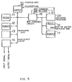
- FIG. 5 there is shown a block diagram illustrating a PLC according to one embodiment of the present invention in which the above-described processor is used.
- an all-purpose processor 10 as commonly used is provided, which carries out numerical computations, processings of function instructions, etc. precluding the overall control of the PLC and the logic operations.
- a RAM 12 stores rewritable data, parameters which are necessary for controlling the entire PLC.
- a programming unit 13 produces a program for controlling a subject to be controlled by the PLC, e.g. a machine tool.
- the programming unit 13 is provided with a display unit for displaying a program and data, and an input unit for inputting the program and the data.
- a display unit for displaying a program and data
- an input unit for inputting the program and the data.
- a display unit a CRT, crystal liquid or the like are used.
- the input unit a keyboard, paper tape reader, cassette tape reader or the like are used.
- the programming unit 13 may be constructed to incorporate therein a software for inputting and outputting those data.
- the software has a function for assembling or compiling the inputted source program to an object format. Such software may be loaded into the ROM 11, or it is possible to implement it with the use of the all-purpose processor 10 or with an exclusive processor provided in the programming unit 13.
- An input/output circuit 14 is an interface connected to the subject to be controlled. This input/output circuit can further be connected to an upper-class host computer, computerized numerical controller, etc.
- a bus command circuit 15 is used for controlling the usage of the bus between the all-purpose processor 10 and an exclusive processor to be described later.
- the exclusive processor 20 as described with reference to Figs. 1 and 2 exclusively executes logic processing.
- the all-purpose processor 10 sends a command to the bus command circuit 15 requesting the use of the bus in the all-purpose processor 20.
- the bus command circuit 15 in turn sends this command to the exclusive processor 20.
- the exclusive processor 20 releases the bus and permits the all-purpose processor 10 to use it at the time when the instructions which the exclusive processor is executing has terminated.
- the exclusive processor 20 receives an instruction other than the logic operations during execution of the instructions, it causes the all-purpose processor 10 to interrupt and transfers that instruction to the all purpose processor 10 to enable it to execute the instruction. In this fashion, the exclusive processor only executes the logic operations at a high speed.
- a memory 16 stores a program (ladder diagram) which the exclusive processor 20 processes, for which a ROM or a battery-backuped RAM is used.
- a program ladder diagram
- the exclusive processor 20 processes, for which a ROM or a battery-backuped RAM is used.
- the program is stored in the battery-backuped RAM and is corrected.
- the complete program is loaded into the ROM for use.
- a RAM 17 stores therein data which are necessary for the exclusive processor 20 to execute the program loaded in the memory 16, and logic data to be subjected to logic processing.
- the exclusive processor 20 executes the program loaded in the memory 16. If it is the logic processing, execution is immediately started. If the program is not directed to the logic operations but a special function instruction, an interruption signal is generated to thereby cause the all-purpose processor 10 to interrupt. In response to the interruption signal, the all-purpose processor 10 issues a command to the bus command circuit 15 requesting the use of the bus. The bus command circuit 15 issues the bus command signal to the exclusive processor 20. In response to the signal from the bus command circuit 15, the exclusive processor 20 releases the bus at a break of the instruction and outputs the bus release signal to the bus command circuit 15. As a result, the all-purpose processor 10 is capable of using the bus of the exclusive processor 20 and executes the special function instruction upon reading it out of the memory 16. When the execution of this instruction is terminated, the control again returns to the exclusive processor 20 and the latter again executes the logic processing.
- the ladder diagram is executed in the following manner.
- the all-purpose processor 10 reads the input signal out of the input/output circuit 14 and the signal thus read out is written into the RAM 17.
- the exclusive processor processes the logic operations of the input data written in the RAN 17 in accordance with the program (ladder diagram) loaded in the memory 16. The resultant data is written into another location of the RAM 17.
- the all-purpose processor 10 reads the operation data out of the RAM 17 and outputs it through the input/output circuit 14.
- the ladder diagram is carried out.
- unnecessary logic operations are excluded and executes only the logic operations, whereby the processing speed can further be increased.
- the invention is arranged so that unnecessary logic operations are omitted in conformity with the kinds of instructions and the result of the logic operation.
- the checking to this effect is implemented simultaneously with the execution of the instructions. Therefore, the logic processes can be performed at a high speed.
- processors as described above can be used as an exclusive processor for executing logic operations, and another processor is employed for executing the remaining instructions, whereby a PLC operable at a high speed can be obtained.
Landscapes
- Physics & Mathematics (AREA)
- General Physics & Mathematics (AREA)
- Engineering & Computer Science (AREA)
- Automation & Control Theory (AREA)
- Programmable Controllers (AREA)
- Executing Machine-Instructions (AREA)
Claims (2)
- Prozessor (1) für einen programmierbaren logischen Regler zur Ausführung von logischen Operationen mit
einer logischen Operationseinrichtung (2) zur Ausführung einer logischen Operation;
einer Sprungzustandsüberprüfungseinrichtung (4) zum Überprüfen, ob eine logische Operation nach einer momentanen logischen Operation auf der Basis der Beziehung zwischen einem resultierenden Wert der momentanen logischen Operation und den durch die unmittelbar nachfolgenden Befehle vorgegebenen Arten von logischen Operationen ausgeführt werden soll oder nicht;
gekennzeichnet durch
eine Sprungverhinderungseinrichtung (3) zur Festlegung, ob in Abhängigkeit von einer speziellen Operation ein Sprung durchgeführt werden kann oder verhindert werden muß; und
eine Sprungausführungseinrichtung (5) zur Ausführung der logischen Operation nach den logischen Operationen, für die die Sprungverhinderungseinrichtung festgelegt hat, daß ein Sprung durchgeführt werden kann, und zwar nur dann, wenn die Sprungzustandsüberprüfungseinrichtung (4) festlegt, daß die logische Operation ausgeführt werden soll. - Programmierbarer logischer Regler mit zwei Prozessoren (20, 10) mit
einem Exklusivprozessor (20) für einen programmierbaren logischen Regler gemäß Anspruch 1, bei dem der Exklusivprozessor logische Operationen ausführt; und
einem zweiten Prozessor (10) zur Ausführung von anderen als logischen Operationen.
Applications Claiming Priority (2)
| Application Number | Priority Date | Filing Date | Title |
|---|---|---|---|
| JP62048408A JPS63214804A (ja) | 1987-03-03 | 1987-03-03 | Plc用プロセツサ及びplc |
| JP48408/87 | 1987-03-03 |
Publications (3)
| Publication Number | Publication Date |
|---|---|
| EP0306535A1 EP0306535A1 (de) | 1989-03-15 |
| EP0306535A4 EP0306535A4 (en) | 1990-12-05 |
| EP0306535B1 true EP0306535B1 (de) | 1994-02-09 |
Family
ID=12802478
Family Applications (1)
| Application Number | Title | Priority Date | Filing Date |
|---|---|---|---|
| EP19880901928 Expired - Lifetime EP0306535B1 (de) | 1987-03-03 | 1988-02-19 | Prozessor für programmierbaren logischen regler und programmierbarer logischer regler |
Country Status (4)
| Country | Link |
|---|---|
| EP (1) | EP0306535B1 (de) |
| JP (1) | JPS63214804A (de) |
| DE (1) | DE3887717T2 (de) |
| WO (1) | WO1988006751A1 (de) |
Families Citing this family (5)
| Publication number | Priority date | Publication date | Assignee | Title |
|---|---|---|---|---|
| JPH02284206A (ja) * | 1989-04-26 | 1990-11-21 | Fanuc Ltd | プログラマブル・コントローラ |
| FR2808601B1 (fr) * | 2000-05-04 | 2002-07-26 | Sagem | Procede de commande d'un organe de vehicule automobile |
| JP2002351509A (ja) * | 2001-05-25 | 2002-12-06 | Mitsubishi Electric Corp | プログラミングツール及びプログラミング方法 |
| KR100781340B1 (ko) * | 2006-09-18 | 2007-11-30 | 삼성전자주식회사 | 사용자 정의 확장 연산을 처리하는 연산 시스템 및 방법 |
| JP2008226276A (ja) * | 2008-06-09 | 2008-09-25 | Matsushita Electric Works Ltd | プログラマブルコントローラ |
Family Cites Families (7)
| Publication number | Priority date | Publication date | Assignee | Title |
|---|---|---|---|---|
| US3753243A (en) * | 1972-04-20 | 1973-08-14 | Digital Equipment Corp | Programmable machine controller |
| JPS5344633B2 (de) * | 1974-04-19 | 1978-11-30 | ||
| JPS555129B2 (de) * | 1974-05-28 | 1980-02-04 | ||
| JPS56111905A (en) * | 1980-02-07 | 1981-09-04 | Mitsubishi Electric Corp | Programmable sequence controller |
| JPS57166605A (en) * | 1981-04-06 | 1982-10-14 | Matsushita Electric Ind Co Ltd | Sequence controller |
| JPS62111303A (ja) * | 1985-11-11 | 1987-05-22 | Mitsubishi Electric Corp | プログラマブルコントロ−ラの制御方式 |
| JPS62154104A (ja) * | 1985-12-27 | 1987-07-09 | Nissan Motor Co Ltd | 入出力信号処理装置 |
-
1987
- 1987-03-03 JP JP62048408A patent/JPS63214804A/ja active Pending
-
1988
- 1988-02-19 EP EP19880901928 patent/EP0306535B1/de not_active Expired - Lifetime
- 1988-02-19 DE DE3887717T patent/DE3887717T2/de not_active Expired - Fee Related
- 1988-02-19 WO PCT/JP1988/000181 patent/WO1988006751A1/ja not_active Ceased
Also Published As
| Publication number | Publication date |
|---|---|
| WO1988006751A1 (fr) | 1988-09-07 |
| EP0306535A1 (de) | 1989-03-15 |
| JPS63214804A (ja) | 1988-09-07 |
| DE3887717T2 (de) | 1994-05-19 |
| EP0306535A4 (en) | 1990-12-05 |
| DE3887717D1 (de) | 1994-03-24 |
Similar Documents
| Publication | Publication Date | Title |
|---|---|---|
| US4328550A (en) | Programmer unit with composite calculation capability | |
| EP0586813B1 (de) | Speicherprogrammierbare Steuerung mit Leiterdiagramm-Makroinstrucktionen | |
| EP0106572B1 (de) | Datenverarbeitungssystem mit virtuellen Maschinen | |
| US3962685A (en) | Data processing system having pyramidal hierarchy control flow | |
| US4034354A (en) | Programmable interface controller for numerical machine systems | |
| US4045782A (en) | Microprogrammed processor system having external memory | |
| US5319783A (en) | Programmable controller with an operator messaging function | |
| DE1474063A1 (de) | Datenverarbeitungsanlage | |
| US5986425A (en) | Numerical controller | |
| EP0306535B1 (de) | Prozessor für programmierbaren logischen regler und programmierbarer logischer regler | |
| US4298933A (en) | Data-processing device including means to suppress the execution of unnecessary instructions | |
| US5233697A (en) | PLC processor and PLC | |
| EP0338317B1 (de) | In Direktabbildung und in Bankabbildung wirksamer Informationsprozessor und Verfahren zum Schalten der Abbildungsschemas | |
| JPS6134605A (ja) | プログラマブルコントロ−ラの制御方式 | |
| JPS5941209B2 (ja) | バイプログラミング可能型電子的会計システム | |
| US3470537A (en) | Information processing system using relative addressing | |
| EP0136699B1 (de) | Programmierbares Steuerwerk | |
| EP0466940B1 (de) | Nebenanschluss einer programmierbaren maschinensteuerung | |
| JP3107308B2 (ja) | 異種言語混在形プログラム処理コントローラ | |
| EP0445288A1 (de) | Betriebsbehandlungseinheit | |
| JP3024719B2 (ja) | プログラマブルコントローラの演算処理方法 | |
| Golding | CATY, a system for experiment control, data collection, data display and analysis | |
| JPS6238746B2 (de) | ||
| JP3341061B2 (ja) | プログラマブルコントローラ | |
| Hintze | The Instruction Code of the Computer |
Legal Events
| Date | Code | Title | Description |
|---|---|---|---|
| PUAI | Public reference made under article 153(3) epc to a published international application that has entered the european phase |
Free format text: ORIGINAL CODE: 0009012 |
|
| 17P | Request for examination filed |
Effective date: 19881201 |
|
| AK | Designated contracting states |
Kind code of ref document: A1 Designated state(s): DE FR GB |
|
| A4 | Supplementary search report drawn up and despatched |
Effective date: 19901018 |
|
| AK | Designated contracting states |
Kind code of ref document: A4 Designated state(s): DE FR GB |
|
| 17Q | First examination report despatched |
Effective date: 19921130 |
|
| GRAA | (expected) grant |
Free format text: ORIGINAL CODE: 0009210 |
|
| AK | Designated contracting states |
Kind code of ref document: B1 Designated state(s): DE FR GB |
|
| PG25 | Lapsed in a contracting state [announced via postgrant information from national office to epo] |
Ref country code: FR Free format text: THE PATENT HAS BEEN ANNULLED BY A DECISION OF A NATIONAL AUTHORITY Effective date: 19940209 |
|
| REF | Corresponds to: |
Ref document number: 3887717 Country of ref document: DE Date of ref document: 19940324 |
|
| PG25 | Lapsed in a contracting state [announced via postgrant information from national office to epo] |
Ref country code: GB Effective date: 19940509 |
|
| EN | Fr: translation not filed | ||
| PLBE | No opposition filed within time limit |
Free format text: ORIGINAL CODE: 0009261 |
|
| STAA | Information on the status of an ep patent application or granted ep patent |
Free format text: STATUS: NO OPPOSITION FILED WITHIN TIME LIMIT |
|
| GBPC | Gb: european patent ceased through non-payment of renewal fee |
Effective date: 19940509 |
|
| 26N | No opposition filed | ||
| PGFP | Annual fee paid to national office [announced via postgrant information from national office to epo] |
Ref country code: DE Payment date: 19970228 Year of fee payment: 10 |
|
| PG25 | Lapsed in a contracting state [announced via postgrant information from national office to epo] |
Ref country code: DE Free format text: LAPSE BECAUSE OF NON-PAYMENT OF DUE FEES Effective date: 19981103 |