EP0307151A1 - Drucker - Google Patents
Drucker Download PDFInfo
- Publication number
- EP0307151A1 EP0307151A1 EP88308186A EP88308186A EP0307151A1 EP 0307151 A1 EP0307151 A1 EP 0307151A1 EP 88308186 A EP88308186 A EP 88308186A EP 88308186 A EP88308186 A EP 88308186A EP 0307151 A1 EP0307151 A1 EP 0307151A1
- Authority
- EP
- European Patent Office
- Prior art keywords
- recording
- recording electrodes
- electrodes
- counterelectrode
- voltage
- Prior art date
- Legal status (The legal status is an assumption and is not a legal conclusion. Google has not performed a legal analysis and makes no representation as to the accuracy of the status listed.)
- Granted
Links
- 230000005684 electric field Effects 0.000 claims abstract description 17
- 230000001105 regulatory effect Effects 0.000 claims abstract description 6
- 239000002245 particle Substances 0.000 claims description 6
- OKTJSMMVPCPJKN-UHFFFAOYSA-N Carbon Chemical compound [C] OKTJSMMVPCPJKN-UHFFFAOYSA-N 0.000 claims description 4
- 239000011230 binding agent Substances 0.000 claims description 4
- 239000000203 mixture Substances 0.000 claims description 4
- 238000005245 sintering Methods 0.000 claims description 4
- 239000010409 thin film Substances 0.000 claims description 4
- 229910052799 carbon Inorganic materials 0.000 claims description 3
- PNEYBMLMFCGWSK-UHFFFAOYSA-N aluminium oxide Inorganic materials [O-2].[O-2].[O-2].[Al+3].[Al+3] PNEYBMLMFCGWSK-UHFFFAOYSA-N 0.000 claims description 2
- 239000004033 plastic Substances 0.000 claims description 2
- 229920003023 plastic Polymers 0.000 claims description 2
- 230000001276 controlling effect Effects 0.000 claims 1
- 239000000463 material Substances 0.000 claims 1
- 229920003002 synthetic resin Polymers 0.000 claims 1
- 239000000057 synthetic resin Substances 0.000 claims 1
- 238000009826 distribution Methods 0.000 abstract description 13
- 230000014509 gene expression Effects 0.000 description 9
- 238000000034 method Methods 0.000 description 6
- 230000003111 delayed effect Effects 0.000 description 4
- 230000001788 irregular Effects 0.000 description 4
- 230000001133 acceleration Effects 0.000 description 2
- 239000003990 capacitor Substances 0.000 description 2
- 238000010276 construction Methods 0.000 description 2
- 238000001125 extrusion Methods 0.000 description 2
- 230000000737 periodic effect Effects 0.000 description 2
- 230000008569 process Effects 0.000 description 2
- 230000009466 transformation Effects 0.000 description 2
- 229930182556 Polyacetal Natural products 0.000 description 1
- 230000001174 ascending effect Effects 0.000 description 1
- 239000011248 coating agent Substances 0.000 description 1
- 238000000576 coating method Methods 0.000 description 1
- 239000004020 conductor Substances 0.000 description 1
- 230000001419 dependent effect Effects 0.000 description 1
- 238000010586 diagram Methods 0.000 description 1
- -1 polyethylene terephthalate Polymers 0.000 description 1
- 229920000139 polyethylene terephthalate Polymers 0.000 description 1
- 239000005020 polyethylene terephthalate Substances 0.000 description 1
- 229920006324 polyoxymethylene Polymers 0.000 description 1
- 230000000630 rising effect Effects 0.000 description 1
Images




Classifications
-
- B—PERFORMING OPERATIONS; TRANSPORTING
- B41—PRINTING; LINING MACHINES; TYPEWRITERS; STAMPS
- B41J—TYPEWRITERS; SELECTIVE PRINTING MECHANISMS, i.e. MECHANISMS PRINTING OTHERWISE THAN FROM A FORME; CORRECTION OF TYPOGRAPHICAL ERRORS
- B41J2/00—Typewriters or selective printing mechanisms characterised by the printing or marking process for which they are designed
- B41J2/005—Typewriters or selective printing mechanisms characterised by the printing or marking process for which they are designed characterised by bringing liquid or particles selectively into contact with a printing material
- B41J2/01—Ink jet
- B41J2/015—Ink jet characterised by the jet generation process
- B41J2/04—Ink jet characterised by the jet generation process generating single droplets or particles on demand
- B41J2/06—Ink jet characterised by the jet generation process generating single droplets or particles on demand by electric or magnetic field
-
- B—PERFORMING OPERATIONS; TRANSPORTING
- B41—PRINTING; LINING MACHINES; TYPEWRITERS; STAMPS
- B41J—TYPEWRITERS; SELECTIVE PRINTING MECHANISMS, i.e. MECHANISMS PRINTING OTHERWISE THAN FROM A FORME; CORRECTION OF TYPOGRAPHICAL ERRORS
- B41J2/00—Typewriters or selective printing mechanisms characterised by the printing or marking process for which they are designed
- B41J2/005—Typewriters or selective printing mechanisms characterised by the printing or marking process for which they are designed characterised by bringing liquid or particles selectively into contact with a printing material
- B41J2/01—Ink jet
- B41J2/07—Ink jet characterised by jet control
- B41J2/075—Ink jet characterised by jet control for many-valued deflection
- B41J2/095—Ink jet characterised by jet control for many-valued deflection electric field-control type
-
- B—PERFORMING OPERATIONS; TRANSPORTING
- B41—PRINTING; LINING MACHINES; TYPEWRITERS; STAMPS
- B41J—TYPEWRITERS; SELECTIVE PRINTING MECHANISMS, i.e. MECHANISMS PRINTING OTHERWISE THAN FROM A FORME; CORRECTION OF TYPOGRAPHICAL ERRORS
- B41J2/00—Typewriters or selective printing mechanisms characterised by the printing or marking process for which they are designed
- B41J2/005—Typewriters or selective printing mechanisms characterised by the printing or marking process for which they are designed characterised by bringing liquid or particles selectively into contact with a printing material
- B41J2/01—Ink jet
- B41J2/015—Ink jet characterised by the jet generation process
- B41J2/04—Ink jet characterised by the jet generation process generating single droplets or particles on demand
- B41J2/06—Ink jet characterised by the jet generation process generating single droplets or particles on demand by electric or magnetic field
- B41J2002/061—Ejection by electric field of ink or of toner particles contained in ink
Definitions
- V2 V4 - i4 x R4 (1)
- V3 V1 - i1 x R1 (2)
- V4 V3 - i3 x R3 (3)
- Q C x (V3 - V4 - i2 x R2) (4)
- dQ/dt i2 (5)
- i1 i2 + i3 (6)
- Table 1 Driving mode Recording electrode 31
- Recording electrode 32 1 OFF ON - OFF - OFF 2 ON OFF - ON - OFF 3 OFF - ON - OFF OFF - ON - OFF OFF - ON - OFF
- V2 and V4 for those modes are determined by the following procedure. The procedure will be described hereinafter with reference to the Mode 1.
- Solution for V4 can be obtained similarly by eliminating i1, i2, i3, Q and V3 from Expressions (1) to (6) to express Expression (7) by V1 and V2.
- Solutions for V3 and V4 for Modes 2 and 3 can also be obtained through the same procedure.
- Voltage pulses thus determined are shown in Figs. 13(a) to 13(d) respectively for V1, V2, V3 and V4 in Mode 1
- Figs. 15(a) to 15(d) respectively for V1, V2, V3 and V4 in Mode 3 in which voltage pulses are applied to one of the two recording electrodes 3 or to both the two recording electrodes 3. More concretely, in Figs.
- the quantity of the ink 1 jetted from the front end 3a of the recording electrode 3 varies to deteriorate the quality of prints, when the recording electrodes 3 are driven under conditions where the waveforms of the surface potentials of the recording electrodes are irregular.
- Fig. 16(a), 16(b) and 16(c) are equifield intensity contour maps showing the distribution of field intensity in electric field produced between the plurality of recording electrodes 3 and the counterelectrode 5, in which indicated at A are equifield intensity curves. In Fig. 16(a), 16(b) and 16(c), only three recording electrodes 3 are shown for simplicity.
- a voltage is applied only to the central recording electrode 3.
- the steepness of the equifield intensity curves A ascending toward the counterelectrode 5 is greater than that of the equifield intensity curves A of Fig. 16(a), and an electric field is produced between the driven recording electrode 3 and the adjacent undriven recording electrodes 3 as well as between the driven recording electrode 3 and the counterelectrode 5.
- a voltage is applied to the central recording electrode 3 and one of the adjacent recording electrode 3 (the left-hand recording electrode 3 as viewed in Fig. 16(c)).
- the steepness of the equifield intensity curves A in Fig. 16(c) is smaller than that of the equifield intensity curves A in Fig. 16(b) and is greater than that of the equifield intensity curves A in Fig. 16(a).
- An electric field is produced, similarly to the state shown in Fig. 16(b), between the driven recording electrode 3 and the undriven recording electrode 3.
- the gradient of the equifield intensity curves A represents the intensity of the electric field.
- Electrostatic force that acts on the ink at the front end of the recording electrode 3 is proportional to the gradient of the equifield intensity curve A, and the greater the gradient of the equifield intensity curve A, the greater is the quantity of ink jetted from the recording electrode 3.
- the quantity of ink jetted in the state shown in fig. 16(b) is greater than that in the state shown in Fig. 16(a). Accordingly, the quantity of ink jetted from the recording electrode 3 is dependent on the operating condition of the adjacent recording electrodes, and hence print quality is unstable.
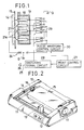
- FIG. 1 A nonimpact printer in a first embodiment according to the present invention will be described hereinafter with reference to Figs. 1 to 8, in which parts like or corresponding to those previously described with reference to Figs. 11 and 12 are based on the same theory as that on which those previously described with reference to Figs. 11 and 12, and hence the description thereof will be omitted and Figs. 11 and 12 will be cited when necessary.
- the recording electrodes 21 are connected electrically to the counterelectrode 14 by a driving circuit 26 comprising a power supply 24 and a switching circuit 25.
- the switching circuit 25 includes a print control circuit 27, a switching signal circuit 28 connected to the print control circuit 27, and switches 29 which are connected respectively to the recording electrodes 21.
- Each switch 29 has a first contact connected to a ground G, and a second contact connected through the power supply 24 to the counterelectrode 14.
- the power supply 24 comprises a first power supply 24a connected to the counterelectrode 14, and a second power supply 24b connected to the recording electrodes 21. The junction of the first power supply 24a and the second power supply 24b is connected to the ground G.
- a pulse waveform control circuit 30 is connected to the respective second contacts of the switches 29, to the second power supply 24b, and to the print control circuit 27.
- the print control circuit 27 controls the pulse waveform control circuit 30 so as to control the waveforms of voltage pulse signals to be applied to the recording electrodes 21 according to a recording electrode driving mode. More concretely,
- the pulse waveform control circuit 30 has, for each recording electrode 21, an input system 31 connected to the power supply 24 and having a circuit construction as shown in Fig. 4.
- the input system 31 has an additional system 31a consisting of a switch A 32 having a contact connected to the ground G, and a resistor R1, and a main system 31b consisting of a switch B 33 and a resistor R4.
- the ink 18 flows into the through hole 22 from the rear end of the recording electrode 21 to fill up the through hole 22 including a portion in the front end 21a of the recording electrode 21.
- the voltage of the first power supply 24a is applied across the recording electrodes 21 and the counterelectrode 14 as a base voltage to exert an electrostatic force on the ink 18 prevailing in the front ends 21a of the recording electrodes 21. This electrostatic force is sufficient to make the ink 18 ready to be jetted, but is not strong enough to accelerate the ink 18 toward the counterelectrode 14.
- each switch 29 Upon the reception of the switching signal, each switch 29 opens the first contact connected to the ground G and closes the second contact connected to the power supply 24 to apply the voltage of the second power supply 24b, which is sufficiently high to jet the ink 18, across the corresponding recording electrode 21 and the counterelectrode 14, and thereby the ink 18 is jetted from the front end 21a of the recording electrode 21 and is deposited in a dot on the recording sheet 15 to form a character.
- a d1-delayed signal 2 on the basis of a print period pulse signal 1 having a period T, a d1-delayed signal 2, a d2-delayed signal 3, a first print signal 4, a first T-delayed signal 5 delayed by T from the print period pulse signal 1, a second print signal 6 for the adjacent recording electrode 21, and a second T-delayed signal 7 delayed by T from the second print signal 6 are prepared.
- the signals 4 to 7 are sampled and a decision is made, and then the switching operation is carried out at the leading edge of the d2-delayed signal 3 on the basis of the decision.
- FIG. 9 showing a print head 13 and the associated electric circuits employed in a nonimpact printer in the second embodiment according to the present invention, in which parts like or corresponding to those previously described with reference to the first embodiment are denoted by the same reference numerals and the description thereof will be omitted.
- the print head 13 has an ink case 19 containing ink 18.
- a plurality of electrode holes 20 are formed in an arrangement in a vertical row in a side wall of the ink case 19 facing a counterelectrode 14.
- a plurality of recording electrodes 21 are placed in the ink case 19 with the respective front ends 21a thereof projecting through the electrode holes 22 toward the counterelectrode 14.
- the ink 18 flows into the through hole 22 of each recording electrode 21 from the rear end of the same to fill up the through hole 22 including a portion in the front end 21a of the recording electrode 21.
- the voltage of the first power supply 24a is applied across the recording electrodes 21 and the counterelectrode 14 as a base voltage to exert an electrostatic force on the ink 18 prevailing in the front ends 21a of the recording electrodes 21. This electrostatic force is sufficient to make the ink 18 ready to be jetted, but is not strong enough to accelerate the ink 18 toward the counterelectrode 14.
- the switching signal circuit 28 gives a switching signal selectively to the switches 29 corresponding to the selected recording electrodes 21 according to a print command signal given thereto by the print control circuit 27.
- each switch 29 Upon the reception of th switching signal, each switch 29 opens the first contact connected to the ground G and closes the second contact connected to the power supply 24 to apply the voltage of the second power supply 24b, which is sufficiently high to jet the ink 18, across the corresponding recording electrode 21 and the counterelectrode 14, and thereby the ink 18 is jetted from the front end 21a of the recording electrode 21 and is deposited in a dot on a recording sheet 15 to form a character.
- the output voltage of the second power supply 24b is regulated properly by the voltage control circuit 35. Since the plurality of recording electrodes 21 are disposed in a close arrangement, the field intensity distribution of an electric field produced between the front end 21a of one of the recording electrodes 21 and the counterelectrode 14 varies according to the operating condition of the adjacent recording electrodes 21, namely, whether or not a voltage is applied to the adjacent recording electrodes 21, as described previously with reference to Figs. 16(a), 16(b) and 16(c). In the second embodiment, the output voltage of the second power supply 24b is regulated properly by the voltage control circuit 35 to maintain the field intensity distribution of the electric field between the recording electrode 21 and the counterelectrode 14 constantly in a specific reference field intensity distribution.
- Each recording electrode 21 employed in the second embodiment is coated with a conductive metallic thin film 23. Therefore, an electric field as shown in Fig. 16(b) or 16(c) is produced between the adjacent recording electrodes 21 when the adjacent recording electrodes 21 are driven simultaneously. This electric field urges the ink 18 stored in the through hole 22 of the recording electrode 21 toward the front end 21a of the recording electrode 21, and thereby an excessive ink 18 is jetted from the recording electrode 21. Accordingly, the voltage control circuit 35 regulates the output voltage of the second power supply 24b taking into consideration such a phenomenon to maintain the quantity of the ink 18 to be jetted by the recording electrode 21 for every printing operation correctly at a fixed value.
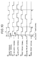
- a d1-delayed signal 2 delayed by d1 from a print period pulse signal 1 having a period T, a d2-delayed signal 3 delayed by d2 from the d1-delayed signal 2, a first print signal 4, a second print signal 5, and a third print signal 6 are prepared on the basis of the print period pulse signal 1.
- the signals 4, 5 and 6 are sampled and a decision is made, and then switching operation according to the result of the decision is carried out at the leading edge of the signal 3 to vary the voltage.
- the delay time d1 is longer than the rising time of the signals 4, 5 and 6, and the delay time d2 is longer than a time necessary for the decision.
- Decisions A, B, C and D in Fig. 10 correspond to the conditions shown in Figs. 16(a), 16(b) and 16(c) as follows.
- a plurality of recording electrodes capable of jetting ink from the respective front ends thereof are mounted on a carriage, a counterelectrode is disposed opposite to the recording electrodes with a recording sheet therebetween, and the pulse waveform of a voltage to be applied to one of the recording electrodes by the driving circuit which applies voltage pulses selectively across the recording electrodes and the counterelectrode is regulated according to the operating condition of other recording electrodes by the pulse waveform control circuit.
- a voltage pulse having a regular waveform is applied to the recording electrode regardless of the operating condition of other recording electrodes, so that a fixed quantity of the ink is jetted from the front end of each recording electrode regardless of the operating condition of the rest of the recording electrodes, and thereby characters are formed in a high print quality.
- a plurality of recording electrodes capable of jetting ink from the respective front ends thereof are mounted on a carriage, a counterelectrode is disposed opposite to the recording electrodes with a recording sheet therebetween, and a voltage to be applied to one of the recording electrodes by the driving circuit which applies a voltage selectively across the recording electrodes and the counterelectrode is regulated according to the operating condition of the adjacent recording electrodes by the voltage control circuit.
- the field intensity distribution of an electric field produced between the recording electrode and the counterelectrode can be maintained in a specific reference field intensity distribution, so that a fixed quantity of the ink is jetted from the front end of the recording electrode for every printing operation, and thereby characters are formed in a high print quality.
Landscapes
- Particle Formation And Scattering Control In Inkjet Printers (AREA)
Applications Claiming Priority (4)
| Application Number | Priority Date | Filing Date | Title |
|---|---|---|---|
| JP22799787A JPS6471761A (en) | 1987-09-11 | 1987-09-11 | Printer |
| JP227998/87 | 1987-09-11 | ||
| JP22799887A JPS6471762A (en) | 1987-09-11 | 1987-09-11 | Printer |
| JP227997/87 | 1987-09-11 |
Publications (2)
| Publication Number | Publication Date |
|---|---|
| EP0307151A1 true EP0307151A1 (de) | 1989-03-15 |
| EP0307151B1 EP0307151B1 (de) | 1992-01-22 |
Family
ID=26527993
Family Applications (1)
| Application Number | Title | Priority Date | Filing Date |
|---|---|---|---|
| EP88308186A Expired EP0307151B1 (de) | 1987-09-11 | 1988-09-05 | Drucker |
Country Status (3)
| Country | Link |
|---|---|
| US (1) | US4864327A (de) |
| EP (1) | EP0307151B1 (de) |
| DE (1) | DE3867979D1 (de) |
Cited By (1)
| Publication number | Priority date | Publication date | Assignee | Title |
|---|---|---|---|---|
| CN102825910A (zh) * | 2011-06-16 | 2012-12-19 | 研能科技股份有限公司 | 驱动控制装置 |
Families Citing this family (2)
| Publication number | Priority date | Publication date | Assignee | Title |
|---|---|---|---|---|
| US6995024B2 (en) * | 2001-08-27 | 2006-02-07 | Sri International | Method and apparatus for electrostatic dispensing of microdroplets |
| US7387352B2 (en) * | 2004-10-19 | 2008-06-17 | Eastman Kodak Company | Print optimization system and method for drop on demand ink jet printers |
Citations (2)
| Publication number | Priority date | Publication date | Assignee | Title |
|---|---|---|---|---|
| EP0195652A1 (de) * | 1985-03-22 | 1986-09-24 | Tokyo Electric Co. Ltd. | Tintenpunktdrucker |
| EP0257985A2 (de) * | 1986-08-27 | 1988-03-02 | Tokyo Electric Co., Ltd. | Leitende Aufzeichnungselektrode für eine Druckvorrichtung |
Family Cites Families (5)
| Publication number | Priority date | Publication date | Assignee | Title |
|---|---|---|---|---|
| JPS6059869B2 (ja) * | 1979-06-22 | 1985-12-27 | 日本電信電話株式会社 | インク記録用ヘツド |
| JPS56170A (en) * | 1979-06-15 | 1981-01-06 | Nippon Telegr & Teleph Corp <Ntt> | Ink recording system |
| JPS61235157A (ja) * | 1985-04-12 | 1986-10-20 | Tokyo Electric Co Ltd | 静電印刷方法 |
| US4710784A (en) * | 1985-07-11 | 1987-12-01 | Tokyo Electric Co., Ltd. | Ink jet printing device |
| JPS6283151A (ja) * | 1985-10-08 | 1987-04-16 | Tokyo Electric Co Ltd | 印刷装置 |
-
1988
- 1988-09-05 DE DE8888308186T patent/DE3867979D1/de not_active Expired - Lifetime
- 1988-09-05 EP EP88308186A patent/EP0307151B1/de not_active Expired
- 1988-09-09 US US07/242,135 patent/US4864327A/en not_active Expired - Fee Related
Patent Citations (2)
| Publication number | Priority date | Publication date | Assignee | Title |
|---|---|---|---|---|
| EP0195652A1 (de) * | 1985-03-22 | 1986-09-24 | Tokyo Electric Co. Ltd. | Tintenpunktdrucker |
| EP0257985A2 (de) * | 1986-08-27 | 1988-03-02 | Tokyo Electric Co., Ltd. | Leitende Aufzeichnungselektrode für eine Druckvorrichtung |
Cited By (2)
| Publication number | Priority date | Publication date | Assignee | Title |
|---|---|---|---|---|
| CN102825910A (zh) * | 2011-06-16 | 2012-12-19 | 研能科技股份有限公司 | 驱动控制装置 |
| CN102825910B (zh) * | 2011-06-16 | 2015-04-01 | 研能科技股份有限公司 | 驱动控制装置 |
Also Published As
| Publication number | Publication date |
|---|---|
| EP0307151B1 (de) | 1992-01-22 |
| US4864327A (en) | 1989-09-05 |
| DE3867979D1 (de) | 1992-03-05 |
Similar Documents
| Publication | Publication Date | Title |
|---|---|---|
| DE69929735T2 (de) | Steuerschaltung eines Tintenstrahldruckkopfes | |
| DE60204180T2 (de) | Flüssigkeitsstrahlvorrichtung und Verfahren zu deren Steuerung | |
| DE69206772T2 (de) | Steuerschaltung für Tintenstrahlaufzeichnungskopf | |
| US6419336B1 (en) | Ink ejector | |
| US5198833A (en) | Variable density ink-jet dot printer | |
| EP0307151A1 (de) | Drucker | |
| EP0761441B1 (de) | Tintenstrahldrucker zur Verwendung von Pigmentteilchen enthaltender Tinte | |
| US5347300A (en) | Ink-jet printer driver | |
| JPH1120154A (ja) | インクジェットプリンタ及びインクジェットプリンタにおけるインク吐出速度調整方法 | |
| EP0315206B1 (de) | Punktdrucker | |
| EP0210048B1 (de) | Verfahren zum Betrieb eines Farbstrahldruckkopfes | |
| US5206667A (en) | Fleming-type ink jet head | |
| JPH03275360A (ja) | インクジェット記録装置のインクエンド検出方式 | |
| JPS58153662A (ja) | インクジエツト記録装置 | |
| US9475281B2 (en) | Method of operating an electrostatic printhead | |
| US5940098A (en) | Ink-jet printer using ink containing pigment particles | |
| DE69604038T2 (de) | Elektrostatische Tintenstrahlvorrichtung | |
| US9630401B2 (en) | Printhead calibration and printing | |
| JP2735030B2 (ja) | インクジェットプリンタ装置 | |
| US6220695B1 (en) | Ink-jet recording device for suppressing excess electrophoretic accumulation of charged particles | |
| US6428149B1 (en) | Electrostatic ink jet recording apparatus | |
| JP2957517B2 (ja) | 静電式インクジェット記録装置 | |
| DE69818572T2 (de) | Tintenstrahlaufzeichnungsgerät und zugehöriges Steuerverfahren | |
| JP2842841B2 (ja) | インクジェット記録装置 | |
| EP0827832A2 (de) | Elektrostatische Tintenstrahlaufzeichnungsvorrichtung |
Legal Events
| Date | Code | Title | Description |
|---|---|---|---|
| PUAI | Public reference made under article 153(3) epc to a published international application that has entered the european phase |
Free format text: ORIGINAL CODE: 0009012 |
|
| 17P | Request for examination filed |
Effective date: 19880908 |
|
| AK | Designated contracting states |
Kind code of ref document: A1 Designated state(s): DE FR GB |
|
| 17Q | First examination report despatched |
Effective date: 19900725 |
|
| GRAA | (expected) grant |
Free format text: ORIGINAL CODE: 0009210 |
|
| AK | Designated contracting states |
Kind code of ref document: B1 Designated state(s): DE FR GB |
|
| REF | Corresponds to: |
Ref document number: 3867979 Country of ref document: DE Date of ref document: 19920305 |
|
| ET | Fr: translation filed | ||
| PLBE | No opposition filed within time limit |
Free format text: ORIGINAL CODE: 0009261 |
|
| STAA | Information on the status of an ep patent application or granted ep patent |
Free format text: STATUS: NO OPPOSITION FILED WITHIN TIME LIMIT |
|
| 26N | No opposition filed | ||
| PGFP | Annual fee paid to national office [announced via postgrant information from national office to epo] |
Ref country code: GB Payment date: 19960827 Year of fee payment: 9 |
|
| PGFP | Annual fee paid to national office [announced via postgrant information from national office to epo] |
Ref country code: FR Payment date: 19960910 Year of fee payment: 9 |
|
| PGFP | Annual fee paid to national office [announced via postgrant information from national office to epo] |
Ref country code: DE Payment date: 19960913 Year of fee payment: 9 |
|
| PG25 | Lapsed in a contracting state [announced via postgrant information from national office to epo] |
Ref country code: GB Free format text: LAPSE BECAUSE OF NON-PAYMENT OF DUE FEES Effective date: 19970905 |
|
| PG25 | Lapsed in a contracting state [announced via postgrant information from national office to epo] |
Ref country code: FR Free format text: THE PATENT HAS BEEN ANNULLED BY A DECISION OF A NATIONAL AUTHORITY Effective date: 19970930 |
|
| GBPC | Gb: european patent ceased through non-payment of renewal fee |
Effective date: 19970905 |
|
| PG25 | Lapsed in a contracting state [announced via postgrant information from national office to epo] |
Ref country code: DE Free format text: LAPSE BECAUSE OF NON-PAYMENT OF DUE FEES Effective date: 19980603 |
|
| REG | Reference to a national code |
Ref country code: FR Ref legal event code: ST |