EP0307574A1 - Lötkopf zum Ein- und Auslöten von Bauelementen - Google Patents
Lötkopf zum Ein- und Auslöten von Bauelementen Download PDFInfo
- Publication number
- EP0307574A1 EP0307574A1 EP88111241A EP88111241A EP0307574A1 EP 0307574 A1 EP0307574 A1 EP 0307574A1 EP 88111241 A EP88111241 A EP 88111241A EP 88111241 A EP88111241 A EP 88111241A EP 0307574 A1 EP0307574 A1 EP 0307574A1
- Authority
- EP
- European Patent Office
- Prior art keywords
- soldering
- soldering head
- head
- component
- components
- Prior art date
- Legal status (The legal status is an assumption and is not a legal conclusion. Google has not performed a legal analysis and makes no representation as to the accuracy of the status listed.)
- Granted
Links
Images

Classifications
-
- B—PERFORMING OPERATIONS; TRANSPORTING
- B23—MACHINE TOOLS; METAL-WORKING NOT OTHERWISE PROVIDED FOR
- B23K—SOLDERING OR UNSOLDERING; WELDING; CLADDING OR PLATING BY SOLDERING OR WELDING; CUTTING BY APPLYING HEAT LOCALLY, e.g. FLAME CUTTING; WORKING BY LASER BEAM
- B23K3/00—Tools, devices or special appurtenances for soldering, e.g. brazing, or unsoldering, not specially adapted for particular methods
-
- H—ELECTRICITY
- H05—ELECTRIC TECHNIQUES NOT OTHERWISE PROVIDED FOR
- H05K—PRINTED CIRCUITS; CASINGS OR CONSTRUCTIONAL DETAILS OF ELECTRIC APPARATUS; MANUFACTURE OF ASSEMBLAGES OF ELECTRICAL COMPONENTS
- H05K13/00—Apparatus or processes specially adapted for manufacturing or adjusting assemblages of electric components
- H05K13/04—Mounting of components, e.g. of leadless components
- H05K13/046—Surface mounting
- H05K13/0465—Surface mounting by soldering
-
- H—ELECTRICITY
- H05—ELECTRIC TECHNIQUES NOT OTHERWISE PROVIDED FOR
- H05K—PRINTED CIRCUITS; CASINGS OR CONSTRUCTIONAL DETAILS OF ELECTRIC APPARATUS; MANUFACTURE OF ASSEMBLAGES OF ELECTRICAL COMPONENTS
- H05K13/00—Apparatus or processes specially adapted for manufacturing or adjusting assemblages of electric components
- H05K13/04—Mounting of components, e.g. of leadless components
- H05K13/0486—Replacement and removal of components
-
- H—ELECTRICITY
- H05—ELECTRIC TECHNIQUES NOT OTHERWISE PROVIDED FOR
- H05K—PRINTED CIRCUITS; CASINGS OR CONSTRUCTIONAL DETAILS OF ELECTRIC APPARATUS; MANUFACTURE OF ASSEMBLAGES OF ELECTRICAL COMPONENTS
- H05K3/00—Apparatus or processes for manufacturing printed circuits
- H05K3/30—Assembling printed circuits with electric components, e.g. with resistors
- H05K3/32—Assembling printed circuits with electric components, e.g. with resistors electrically connecting electric components or wires to printed circuits
- H05K3/34—Assembling printed circuits with electric components, e.g. with resistors electrically connecting electric components or wires to printed circuits by soldering
- H05K3/3494—Heating processes for reflow soldering
Definitions
- the invention relates to a soldering head for soldering or unsoldering components, in particular for surface-mountable components (SMD).
- SMD surface-mountable components
- the devices available on the market in no way have a parallax-free observation device with which the soldering or desoldering position on the circuit board can be observed.
- the object of the invention is to provide a soldering head for soldering or unsoldering components, which avoids parallax errors when soldering or unsoldering components on a printed circuit board.
- microscopes are generally used in the soldering or unsoldering machines used to observe the soldering or unsoldering process, it is very important that viewing from the top is made possible, since any other procedure, e.g. Viewing at an acute angle from the side, associated with a parallax error. With the dimension of the components and especially that of the connection legs, for the observation of which a microscope must already be used, this is of essential importance.
- the constructive realization provides that a component on a circuit board can be viewed vertically from above through the soldering or unsoldering head.
- the soldering head has corresponding cutouts, which are equivalent to a viewing slot, and at least one viewing window in order to be able to direct the heat provided for soldering or unsoldering on the soldering head to the component and at the same time to allow the component to be viewed.
- soldering head can be easily combined with heating by hot gas.
- the hot gas provided by a peripheral device is usually introduced laterally into the soldering head and passed through the soldering head onto the component or onto its connecting legs.
- soldering heads are essentially made of stainless steel, since this material is in relation to alternative materials, e.g. Aluminum, has a relatively low thermal conductivity.
- the inner surfaces of a viewing shaft can be well anti-reflective when using stainless steel, so that no errors due to reflections are possible when considering the soldering.
- stainless steel also prevents oxidation due to solder vapors, since common solder material does not bind to stainless steel.
- one embodiment of the invention is the use of an inclined rotary plate which can accommodate several soldering heads and each locks one of them in its working position.
- This soldering head is approximately vertical, the component below the soldering head being able to be viewed vertically from above through an optical system through the soldering head.
- the soldering head is in the three Ko Ordinary directions freely movable. This is usually done by an x / y table that moves the component and the printed circuit board in the x and y directions and by a lifting device that acts on the soldering head with respect to the height adjustment.
- a soldering or desoldering machine is shown schematically. It contains the following essential parts: - the soldering head 1 - the turntable 2 - the printed circuit board 3 an SMD component 13 - A dosing device 4 for solder paste with - Compressed air connection 5 and - Lift cylinder 6, as well - Viewing window 8 - Optics 7, here a microscope - A stand 12 for the optics 7 and dosing device 4th - A tripod 11 for the turntable 2 with a lifting device 14 - a vacuum line 15 a lifting cylinder 9 - A hot gas supply 10.
- soldering head 1 attached to the turntable 2 via a cantilever arm is positioned and locked in its working position in such a way that the SMD component 13 is seen from above by means of the optics 7 the viewing window 8 and can be viewed through the soldering head.
- various soldering heads attached to it via extension arms can be made available and swiveled into the working position. Only a second extension arm is shown, but it is not provided with a soldering head 1.
- a hot gas is supplied to the soldering head 1 via the hot gas supply 10, which is passed in the soldering head 1 onto the connecting legs of the SMD component 13 and these, as well as their corresponding connection spots, to the required soldering temperature of, for example, 210 ° or 225 ° C. heated.
- the centering jaws contained in the soldering head 1 are actuated, which temporarily center and hold the SMD component 13.
- a further mounting of the SMD component 13 on the soldering head 1 is provided by a vacuum device which is supplied via a vacuum line 15.
- the exact positioning of the soldering head 1 relative to the SMD component 13 takes place on the one hand through the possible displacement of the printed circuit board 3 in the x / y direction, and via the lifting device 14, which adjusts the height of the soldering head.
- the dosing device 4 is supplied via the compressed air connections 5 and moved vertically upwards or downwards by the lifting cylinder 6 in order to apply a precisely dosed quantity of solder paste to the printed circuit board.
- the optics 7, together with the vertical view through the soldering head 1, enable parallax-free viewing of the soldering or unsoldering area. For this purpose, only the connecting legs of the SMD component 13 are generally visible through the optics 7.
- the centrally seated body of the SMD component 13 is covered by the vacuum device, which temporarily holds the component.
- Such a soldering or unsoldering machine for SMD components 13 can be automated through the use of computer programs. For this, three essential work steps have to be named - the desoldering, the dosing of the solder paste, the soldering of a new SMD component.
- the soldering head 1 is moved approx. 20 mm over the SMD component 13 and then approximated to approx. 1 to 2 mm via a fine adjustment and aligned in the x / y direction so that it is directly above the component.
- the connecting legs of the SMD component 13 are heated from room temperature at a rate of approximately 1.5 ° C. per second to approximately 200 ° C. by means of the hot gas 10 guided over the soldering head.
- the soldering head 1 is then placed on the component 13 and the vacuum is switched on, as a result of which the component is sucked and held on the soldering head.
- the temperature is increased from 200 to 210 ° C or, for example, 225 ° C within 5 to 15 seconds and the solder flows.
- the soldering head then lifts off with the component.
- the numerical values given refer to the use of a normal solder paste.
- soldering head 1 When the soldering head 1 is swiveled into or out of the working position, an exactly metered amount of solder paste is applied to the connection spots on the printed circuit board 3 via the metering device 4.
- the metering device 4 is lowered to a distance of approximately 1 to 2 mm from the printed circuit board 3.
- the lifting cylinder 6 ensures the lowering of a metering needle of the metering device 4.
- the amount of solder paste required can be controlled via the pressure in the compressed air supply 5, over time or via the diameter of the metering needle.
- Soldering is done in the same way as desoldering.
- the SMD component 13 is picked up by the soldering head 1, centered by means of centering jaws and held in place by means of a vacuum.
- the centering jaws are released again in this state. After a rough positioning, it is lowered onto the circuit board and fine-tuned, with the Opitk 7 is checked.
- preheating takes place at a rate of approx. 1.5 ° C per second to approx. 200 ° C and, for example, when using a commercially available solder paste, it is heated to approx. 225 ° C within a further 5 to 15 seconds .
- the holder by suction using a vacuum is then switched off, and at the same time, in order to avoid reheating the body of the SMD components 13, cold air is blown directly onto the SMD component via the vacuum line for about 10 seconds.
- the soldering head 1 now lifts off and the soldering process is finished.
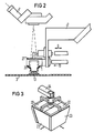
- FIG. 2 A detailed illustration of the soldering head 1 with built-in viewing windows 21 can be seen in FIG. 2, the SMD component 13, which is located on the printed circuit board 3, being viewed vertically from above via the optics 7.
- the turntable 2, the hot gas supply 10 and the lifting cylinder 9 for actuating the centering jaws can also be seen.
- Fig. 3 shows an embodiment of a soldering head with a holder 24, a viewing window 22 and with two mutually perpendicular centering jaw pairs 23, the movements that can be generated by the lifting cylinder 9 for centering and gripping SMD components 13 are indicated by arrows.
Landscapes
- Engineering & Computer Science (AREA)
- Manufacturing & Machinery (AREA)
- Microelectronics & Electronic Packaging (AREA)
- Mechanical Engineering (AREA)
- Electric Connection Of Electric Components To Printed Circuits (AREA)
Abstract
Description
- Die Erfindung betrifft einen Lötkopf zum Ein- oder Auslöten von Bauelementen, insbesondere für oberflächenmontierbare Bauelemente (SMD).
- Bei der Fertigung von elektronischen Flachbaugruppen ist in der letzten Zeit ein Übergang von der herkömmlichen Technik der Einsteckmontage zur Technik der Oberflächenmontage von flach auflötbaren Bauelementen zu verzeichnen. Die hierbei eingesetzten oberflächenmontierbaren Bauelemente (SMD =̂ Surface Mounted Devices) werden durch Bestückautomaten auf den Leiterplatten positioniert, meistens mittels mehrerer Klebstoffpunkte fixiert und anschließend durch ein übliches Lötverfahren verlötet, womit die elektrische Verbindung hergestellt ist. Die bei derartigen Verfahren auftretenden Fehler, sei es durch Einbau falscher oder defekter Bauelemente oder zum Beispiel durch falsche Positionierung, müssen in einem seperaten Verfahren durch Auslöten der entsprechenden Bauelemente und entsprechender Korrektur durch fehlerfreies Einlöten von neuen Bauelementen beseitigt werden. Dies geschieht mittels Vorrichtungen, die man im allgemeinen als Ein- und Auslötmaschinen bezeichnet. Derartige auf dem Markt erhältiche Maschinen müssen einer Vielzahl von Qualitätsanforderungen genügen. So ist es erforderlich, daß der Platz eines defekten Bauelementes, welches ausgelötet und durch fehlerfreies Einlöten eines funktionsfähigen Bauelementes ersetzt werden soll, ohne Behinderungen und ohne Parallaxen-Fehler zu betrachten ist. Des weiteren muß die Heizeinrichtung, mit der die Anschlußbeine des Bauelementes zum Aus- oder Einlöten beheizt werden, eine gleichmäßige Temperaturverteilung über die verschiedenen Anschlußbeine aufweisen und darf zugleich den Körper des Bauelementes nicht zu sehr erhitzen. Ebenso werden hohe Anforderungen an die Ausrichtung des Bauelementes bezüglich der Leiterplatte und des Lötplatzes, an die exakte Dosierung von Lotpaste, an die Kühlung des Bauelementes nach dem Einlöten, sowie an die Hand habung eines durch den Bestückautomaten aufgeklebten Bauelementes beim Auslöten in der Ein- oder Auslötmaschine gestellt.
- Die auf dem Markt erhältlichen Geräte weisen in keiner Weise eine parallaxenfreie Beobachtungseinrichtung auf, mit der der Ein-oder Auslötplatz auf der Leiterplatte beobachtet werden kann.
- Der Erfindung liegt die Aufgabe zugrunde, einen Lötkopf zum Ein- oder Auslöten von Bauelementen bereitzustellen, der Parallaxen-Fehler beim Ein- oder Auslöten von Bauelementen auf einer Leiterplatte vermeidet.
- Die Lösung dieser Aufgabe wird durch den kennzeichnenden Teil des Anspruches 1 beschrieben.
- Da bei den verwendeten Ein- oder Auslötmaschinen in der Regel Miskroskope verwendet werden, um den Ein- oder Auslötvorgang zu betrachten, ist es ganz wesentlich, daß eine Betrachtung senkrecht von oben ermöglicht wird, da jede andere Vorgehensweise, wie z.B. Betrachtung in einem spitzen Winkel von der Seite, mit einem Parallaxen-Fehler verbunden ist. Bei der Dimension der Bauteile und vor allem der der Anschlußbeine, zu deren Betrachtung schon ein Mikroskop eingesetzt werden muß, ist dies von wesentlicher Bedeutung.
- Die konstruktive Verwirklichung sieht vor, daß ein Bauelement auf einer Leiterplatte senkrecht von oben durch den Ein- oder Auslötkopf hindurch betrachtet werden kann. Dazu besitzt der Lötkopf entsprechende Aussparungen, die einem Sichtschacht gleichkommen, und mindestens ein Sichtfenster um die zum Einoder Auslöten am Lötkopf bereitgestellte Wärme gezielt auf das Bauteil führen zu können und gleichzeitig die Betrachtung des Bauteiles zu ermöglichen.
- Weitere vorteilhafte Ausgestaltungen der Erfindung sind den Ansprüchen 2 bis 9 zu entnehmen.
- Besondere hieraus resultierende Vorteile sind zum einen, daß sich die oben beschriebene Gestaltung des Lötkopfes gut mit einer Beheizung durch Heißgas kombinieren läßt. Das von einem Pheripheriegerät bereitgestellte Heißgas wird meist seitlich in den Lötkopf eingeführt und durch den Lötkopf auf das Bauelement bzw. auf dessen Anschlußbeine geleitet. Um wesentliche Temperaturverluste zu vermeiden, sind derartige Lötköpfe im wesentlichen aus Edelstahl gefertigt, da dieser Werkstoff im Verhältnis zu alternativen Werkstoffen, wie z.B. Aluminium, eine relativ geringe Wärmeleitfähigkeit aufweist.
- Zum anderen können die Innenflächen eines Sichtschachtes bei der Verwendung von Edelstahl durch Sandstrahlen gut entspiegelt werden, so daß bei der Betrachtung der Lötung keinerlei Fehler durch Spiegelungen möglich sind.
- Der Einsatz von Edelstahl verhindert weiterhin eine Oxidation durch Lötmitteldämpfe, da übliches Lotmaterial sich nicht mit Edelstahl bindet.
- Die Werkstoffauswahl bezüglich der hitzebeständigen transparenten Sichtfenster hat ergeben, daß am besten Quarzglas verwendet wird, welches mit Silikon gegenüber dem Edelstahl eingedichtet ist.
- Zur einfachen Handhabung beim Aus- oder Einlöten von mehreren Bauelementen, die sich in ihrer Form und Größe auch unterscheiden können, ist eine Ausgestaltung der Erfindung der Einsatz eines schrägstehenden Drehtellers, der mehrere Lötköpfe aufnehmen kann und jeweils einen davon in dessen Arbeitsstellung arretiert. Dieser Lötkopf steht annähernd senkrecht, wobei das Bauelement unterhalb des Lötkopfes senkrecht von oben durch eine Optik durch den Lötkopf hindurch betrachtet werden kann.
- Zur exakten Positionierung des Lötkopfes bezüglich des Bauelementes oder der Leiterplatte ist der Lötkopf in den drei Ko ordianten Richtungen frei bewegbar. Dies geschieht in der Regel durch einen x/y-Tisch, der Bauelement und Leiterplatte in x- und in y-Richtung bewegt und durch eine Hubeinrichtung, die auf den Lötkopf bezüglich der Höhenverstellung wirkt.
- Im folgenden wird anhand von schematischen Figuren ein Ausführungsbeispiel beschrieben.
- Fig. 1 zeigt eine Ein- oder Auslötmaschine für SMD-Bauelemente 13 auf einer Leiterplatte 3.
- Fig. 2 zeigt einen Lötkopf 1 in einer detaillierteren Darstellung.
- Fig. 3 zeigt einen Lötkopf 1 mit Sichtschacht, Fenster 22 und zwei Zentrierbackenpaaren 23.
- In der Fig. 1 ist schematisch eine Ein- oder Auslötmaschine dargestellt. Sie enthält folgende wesentlichen Teile:
- den Lötkopf 1
- den Drehteller 2
- die Leiterplatte 3
- ein SMD-Bauelement 13
- eine Dosiervorrichtung 4 für Lotpaste mit
- Druckluftanschluß 5 und
- Hubzylinder 6, sowie
- Sichtfenster 8
- eine Optik 7, hier ein Mikroskop
- ein Stativ 12 für die Optik 7 und Dosiervorrichtung 4
- ein Stativ 11 für den Drehteller 2 mit
- einer Hubeinrichtung 14
- eine Vakuumleitung 15
- einen Hubzylinder 9
- eine Heißgaszuführung 10. - Der am Drehteller 2 über einen Auslegearm befestigte Lötkopf 1 ist in seiner Arbeitsstellung derart positioniert und arretiert, daß mittels der Optik 7 das SMD-Bauelement 13 von oben durch das Sichtfenster 8 und durch den Lötkopf hindurch betrachtet werden kann. Durch Drehen des Drehtellers 2 können verschiedene an ihm über Auslegearme befestigte Lötköpfe bereit gestellt und in Arbeitsposition geschwenkt werden. Dargestellt ist lediglich ein zweiter Auslegearm, der jedoch nicht mit einem Lötkopf 1 versehen ist. Zum Ein- oder Auslöten wird über die Heißgaszuführung 10 dem Lötkopf 1 ein Heißgas zugeführt, daß im Lötkopf 1 auf die Anschlußbeine des SMD-Bauteils 13 geleitet wird und diese, sowie deren entsprechende Anschlußflecken auf die nötige Löttemperatur von beispielsweise 210° oder 225° C erhitzt. Über den Hubzylinder 9 werden die im Lötkopf 1 enthaltenen Zentrierbacken betätigt, die das SMD-Bauelement 13 zeitweise zentrieren und festhalten. Eine weitere Halterung des SMD-Bauelementes 13 am Lötkopf 1 ist durch eine Vakuumeinrichtung gegeben, die über eine Vakuumleitung 15 versorgt wird. Die exakte Positionierung des Lötkopfes 1 relativ zu dem SMD-Bauelement 13 geschieht zum einen durch die in x/y-Richtung mögliche Verschiebung der Leiterplatte 3, sowie über die Hubeinrichtung 14, die den Lötkopf bezüglich der Höhe einstellt. Die Dosiervorrichtung 4 wird über die Druckluftanschlüsse 5 versorgt und durch den Hubzylinder 6 zum Aufbringen einer genau dosierten Menge von Lotpaste auf die Leiterplatte senkrecht nach oben oder nach unten bewegt. Auch hier ermöglicht die Optik 7 zusammen mit der senkrechten Betrachtungsweise durch den Lötkopf 1 hindurch eine parallaxenfreie Betrachung des Ein- oder Auslötplatzes. Hierzu sind durch die Optik 7 in der Regel nur die Anschlußbeine des SMD-Bauteiles 13 sichtbar. Der zentral sitzende Körper des SMD-Bauteiles 13 ist durch die Vakuumeinrichtung verdeckt, die das Bauteil zeitweise hält.
- Eine derartige Ein- oder Auslötmaschine für SMD-Bauteile 13 ist durch den Einsatz von Computerprogrammen automatisierbar. Hierzu sind drei wesentliche Arbeitsschritte zu benennen - das Auslöten, das Dosieren der Lotpaste, das Einlöten eines neuen SMD-Bauteiles.
- Der Ablauf ist wie folgt:
- Über eine Grobjustierung wird der Lötkopf 1 ca. 20 mm über das SMD-Bauteil 13 gefahren und anschließend über eine Feinjustierung auf ca. 1 bis 2 mm angenähert und in x/y-Richtung ausgerichtet, so daß er direkt über dem Bauteil steht. Mittels des über den Lötkopf geführten Heißgases 10 werden die Anschlußbeine des SMD-Bauelementes 13 von Raumtemperatur mit einer Geschwindigkeit von etwa 1,5° C pro Sekunde bis auf ca. 200° C aufgeheizt. Anschließend wird der Lötkopf 1 auf das Bauelement 13 abgesetzt und das Vakuum eingeschaltet, wodurch das Bauelement am Lötkopf angesaugt und gehalten wird. Während des nun einsetzenden eigentlichen Auslötprozesses wird innerhalb von 5 bis 15 Sekunden die Temperatur von 200 bis 210° C oder beispielsweise 225° C erhöht und das Lot zum Fließen gebracht. Der Lötkopf hebt anschließend mit dem Bauelement ab. Die angegebenen Zahlenwerte beziehen sich auf den Einsatz einer üblichen Lotpaste.
- Bei in Arbeitsposition eingeschwenktem oder auch ausgeschwenktem Lötkopf 1 wird über die Dosiervorrichtung 4 eine exakt dosierte Menge Lotpaste auf die Anschlußflecken auf der Leiterplatte 3 aufgebracht. Dazu wird die Dosiervorrichtung 4 bis auf einen Abstand von ca. 1 bis 2 mm zur Leiterplatte 3 abgesenkt. Der Hubzylinder 6 sorgt für das Absenken einer Dosiernadel der Dosiervorrichtung 4. Die Menge der notwendigen Lotpaste kann über den Druck in der Druckluftzuführung 5, über die Zeit oder über den Durchmesser der Dosiernadel gesteuert werden.
- Das Einlöten geschieht in entsprechender Weise wie das Auslöten. Das SMD-Bauelement 13 wird von dem Lötkopf 1 aufgenommen, mittels Zentrierbacken zentriert und über ein Vakuum festgehalten. Die Zentrierbacken sind in diesem Zustand wieder gelöst. Nach einer Grobpositionierung erfolgt das Absenken auf die Leiterplatte und die Feinjustierung, wobei mit der Opitk 7 kontrolliert wird. Innerhalb der ersten Phase des Aufheizens wird wiederum mit einer Geschwindigkeit von ca. 1,5° C pro Sekunde bis auf ca. 200° C vorgeheizt und beispielsweise beim Einsatz einer handelsüblichen Lotpaste innerhalb von weiteren 5 bis 15 Sekunden auf ca. 225° C erhitzt. Die Halterung durch Ansaugen mittels Vakuum wird anschließend abgeschaltet, wobei gleichzeitig, um eine Nacherhitzung des Körpers der SMD-Bauteile 13 zu vermeiden, etwa 10 Sekunden lang kalte Luft direkt über die Vakuumleitung auf das SMD-Bauelement geblasen wird. Der Lötkopf 1 hebt nun ab und der Einlötvorgang ist beendet.
- In der Fig. 2 ist in einer detallierteren Darstellung der Lötkopf 1 mit eingebauten Sichtfenstern 21 erkennbar, wobei das SMD-Bauteil 13, welches sich auf der Leiterplatte 3 befindet über die Optik 7 senkrecht von oben zu betrachten ist. Der Drehteller 2, die Heißgaszuführung 10 und der Hubzylinder 9 für die Betätigung der Zentrierbacken sind ebenfalls zu erkennen.
- Die Fig. 3 zeigt eine Ausführung eines Lötkopfes mit einer Halterung 24, einem Sichtfenster 22 und mit zwei senkrecht zueinander stehenden Zentrierbackenpaaren 23, deren durch den Hubzylinder 9 erzeugbare Bewegungen zum Zentrieren und Greifen von SMD-Bauelementen 13 durch Pfeile angedeutet sind.
Claims (9)
dadurch gekennzeichnet,
daß der Lötkopf (1) mindestens einen annähernd vertikal zu Leiterplatte (3) und Bauelement (13) stehenden Sichtschacht mit mindestens einem Sichtfenster (21;22) zur Betrachtung der Lötung aufweist.
dadurch gekennzeichnet,
daß der Sichtschacht zugleich ein Heißgasschacht ist.
dadurch gekennzeichnet,
daß das Material des Lötkopfes (1) im wesentlichen Edelstahl ist.
dadurch gekennzeichnet,
daß die Innenflächen eines Sichtschachtes entspiegelt sind.
dadurch gekennzeichnet,
daß das Sichtfenster (21;22) aus hitzebeständigem transparentem Material besteht.
dadurch gekennzeichnet,
daß das hitzebeständige Material Quarzglas ist.
dadurch gekennzeichnet,
daß das Sichtfenster mit Silikon eingedichtet ist.
gekennzeichnet durch
Anordnung auf einem schräg stehenden Drehteller (2), wobei mindestens zwei Lötköpfe (1) montierbar sind und jeweils einer davon in seiner Arbeitsstellung senkrecht steht und arretierbar ist.
dadurch gekennzeichnet,
daß der Lötkopf (1) relativ zu Leiterplatte (3) und Bauelement (13) in den drei Koordinatenrichtungen frei bewegbar ist.
Priority Applications (1)
| Application Number | Priority Date | Filing Date | Title |
|---|---|---|---|
| AT88111241T ATE91064T1 (de) | 1987-08-31 | 1988-07-13 | Loetkopf zum ein- und ausloeten von bauelementen. |
Applications Claiming Priority (2)
| Application Number | Priority Date | Filing Date | Title |
|---|---|---|---|
| DE3729042 | 1987-08-31 | ||
| DE3729042 | 1987-08-31 |
Publications (2)
| Publication Number | Publication Date |
|---|---|
| EP0307574A1 true EP0307574A1 (de) | 1989-03-22 |
| EP0307574B1 EP0307574B1 (de) | 1993-06-23 |
Family
ID=6334880
Family Applications (1)
| Application Number | Title | Priority Date | Filing Date |
|---|---|---|---|
| EP88111241A Expired - Lifetime EP0307574B1 (de) | 1987-08-31 | 1988-07-13 | Lötkopf zum Ein- und Auslöten von Bauelementen |
Country Status (3)
| Country | Link |
|---|---|
| EP (1) | EP0307574B1 (de) |
| AT (1) | ATE91064T1 (de) |
| DE (1) | DE3881992D1 (de) |
Cited By (4)
| Publication number | Priority date | Publication date | Assignee | Title |
|---|---|---|---|---|
| EP0539851A1 (de) * | 1991-11-01 | 1993-05-05 | Smh Engineering Ag | Verfahren zum Verloten eines elektronischen Bauelementes auf einem Substrat und Lotvorrichtung mit einem mit spreizbaren thermoden Lötkopf zur Durchführung dieses Lötverfahren |
| FR2683754A1 (fr) * | 1991-11-15 | 1993-05-21 | Smh Engineering Ag | Procede de soudage d'un composant electronique sur un substrat et dispositif de soudage comprenant une tete de soudage avec des thermodes ecartables permettant la mise en óoeuvre de ce procede de soudage. |
| EP0845807A3 (de) * | 1996-11-27 | 1999-04-07 | Sharp Kabushiki Kaisha | Verfahren zur Herstellung einer elektronischen Schaltungsanordnung, Lehre, um die Lötrückstände gleichförmig zu machen, Lehre zur Übertragung von Lötpaste und Vorrichtung zur Herstellung einer elektronischen Schaltungsvorrichtung |
| DE102012106942A1 (de) * | 2012-07-30 | 2014-01-30 | Endress + Hauser Flowtec Ag | Verfahren zum Austauschen mindestens einer auf einem Träger angeordneten elektronischen Komponente |
Citations (4)
| Publication number | Priority date | Publication date | Assignee | Title |
|---|---|---|---|---|
| CH321976A (fr) * | 1955-02-19 | 1957-05-31 | Ischi Francis | Dispositif auxiliaire pour l'exécution sur tour paralléle de perçages nécessitant successivement l'emploi de plusieurs outils |
| US3912153A (en) * | 1974-11-18 | 1975-10-14 | Gen Motors Corp | Method and apparatus for bonding semiconductor pill-type components to a circuit board |
| US4295596A (en) * | 1979-12-19 | 1981-10-20 | Western Electric Company, Inc. | Methods and apparatus for bonding an article to a metallized substrate |
| EP0040669A1 (de) * | 1980-05-22 | 1981-12-02 | International Business Machines Corporation | Verfahren zum Eliminieren von Lothöckern, die auf einem keramischen Substrat nach der Entfernung eines Halbleiterchips zurückblieben, durch Absorption in einem porösen Kupferblock und Anwendung in der Wiederaufarbeitung von Modulen |
-
1988
- 1988-07-13 EP EP88111241A patent/EP0307574B1/de not_active Expired - Lifetime
- 1988-07-13 AT AT88111241T patent/ATE91064T1/de not_active IP Right Cessation
- 1988-07-13 DE DE8888111241T patent/DE3881992D1/de not_active Expired - Fee Related
Patent Citations (4)
| Publication number | Priority date | Publication date | Assignee | Title |
|---|---|---|---|---|
| CH321976A (fr) * | 1955-02-19 | 1957-05-31 | Ischi Francis | Dispositif auxiliaire pour l'exécution sur tour paralléle de perçages nécessitant successivement l'emploi de plusieurs outils |
| US3912153A (en) * | 1974-11-18 | 1975-10-14 | Gen Motors Corp | Method and apparatus for bonding semiconductor pill-type components to a circuit board |
| US4295596A (en) * | 1979-12-19 | 1981-10-20 | Western Electric Company, Inc. | Methods and apparatus for bonding an article to a metallized substrate |
| EP0040669A1 (de) * | 1980-05-22 | 1981-12-02 | International Business Machines Corporation | Verfahren zum Eliminieren von Lothöckern, die auf einem keramischen Substrat nach der Entfernung eines Halbleiterchips zurückblieben, durch Absorption in einem porösen Kupferblock und Anwendung in der Wiederaufarbeitung von Modulen |
Non-Patent Citations (1)
| Title |
|---|
| IBM TECHNICAL DISCLOSURE BULLETIN, Band 26, Nr. 9. Februar 1984, Seiten 4780-4782, New York, US; A.R. FORMICHELLI et al.: "Non-destructive torsional chip removal" * |
Cited By (6)
| Publication number | Priority date | Publication date | Assignee | Title |
|---|---|---|---|---|
| EP0539851A1 (de) * | 1991-11-01 | 1993-05-05 | Smh Engineering Ag | Verfahren zum Verloten eines elektronischen Bauelementes auf einem Substrat und Lotvorrichtung mit einem mit spreizbaren thermoden Lötkopf zur Durchführung dieses Lötverfahren |
| FR2683754A1 (fr) * | 1991-11-15 | 1993-05-21 | Smh Engineering Ag | Procede de soudage d'un composant electronique sur un substrat et dispositif de soudage comprenant une tete de soudage avec des thermodes ecartables permettant la mise en óoeuvre de ce procede de soudage. |
| EP0845807A3 (de) * | 1996-11-27 | 1999-04-07 | Sharp Kabushiki Kaisha | Verfahren zur Herstellung einer elektronischen Schaltungsanordnung, Lehre, um die Lötrückstände gleichförmig zu machen, Lehre zur Übertragung von Lötpaste und Vorrichtung zur Herstellung einer elektronischen Schaltungsvorrichtung |
| US6062460A (en) * | 1996-11-27 | 2000-05-16 | Sharp Kabushiki Kaisha | Apparatus for producing an electronic circuit |
| DE102012106942A1 (de) * | 2012-07-30 | 2014-01-30 | Endress + Hauser Flowtec Ag | Verfahren zum Austauschen mindestens einer auf einem Träger angeordneten elektronischen Komponente |
| DE102012106942A8 (de) * | 2012-07-30 | 2014-04-10 | Endress + Hauser Flowtec Ag | Verfahren zum Austauschen mindestens einer auf einem Träger angeordneten elektronischen Komponente |
Also Published As
| Publication number | Publication date |
|---|---|
| EP0307574B1 (de) | 1993-06-23 |
| ATE91064T1 (de) | 1993-07-15 |
| DE3881992D1 (de) | 1993-07-29 |
Similar Documents
| Publication | Publication Date | Title |
|---|---|---|
| DE2834836C2 (de) | Vorrichtung zum Herstellen einer Hybrid-Leiterplatte durch Aufbringen elektronischer Bauelemente auf ein Substrat | |
| DE2055360A1 (de) | Verfahren und Vorrichtung zum Ausnch ten und Loten mikrominiaturisierter Schal tungsplattchen | |
| DE102022109905A1 (de) | Verfahren und Vorrichtung zum Löten eines elektronischen Bauteils an eine Schaltkreisplatine, Computerprogrammprodukt und computerlesbares Medium | |
| DE3905291A1 (de) | Vorrichtung zum entfernen und anbringen elektronischer bauelemente von bzw. an einem substrat | |
| DE1941057A1 (de) | Einrichtung zur Lageeinstellung eines Gegenstandes relativ zu einem Bezugspunkt | |
| DE69724894T2 (de) | Bestückungsverfahren von bauelementen auf einem substrat und bestückautomat dafür | |
| DE19501678C2 (de) | Verfahren zum Bestücken von Leiterplatten mit gleichzeitigem Klebstoffauftrag und visueller Erfassung des zu bestückenden Bauteils | |
| EP0420050B1 (de) | Verfahren zum Auflöten von Bauelementen auf Leiterplatten | |
| EP0307574B1 (de) | Lötkopf zum Ein- und Auslöten von Bauelementen | |
| EP0005727B1 (de) | Abfühlvorrichtung zum Feststellen des Ortes von elektrisch leitenden Punkten | |
| DE4105874C1 (de) | ||
| EP0309665B1 (de) | Lötkopf zum Ein- oder Auslöten von Bauelementen mittels einer Beheizung durch Heissgas, insbesondere für oberflächenmontierbare Bauelemente (SMD) | |
| EP0305698B1 (de) | Dosiervorrichtung zum Aufbringen einer Lotpaste auf eine Leiterplatte für das Einlöten von SMD-Bauteilen | |
| EP0305697B1 (de) | Verfahren zum Einlöten von SMD-Bauteilen, die zeitweise an einem mittels Vakuumleitung evakuierbaren Lötkopf gehalten werden | |
| EP0343374A1 (de) | Verfahren zur Reparatur von Leiterbahnunterbrechungen mittels deckungsgleicher Formteile | |
| EP0305696B1 (de) | Verfahren zum Auslöten von aufgeklebten SMD-Bauteilen | |
| EP0305695B1 (de) | Lötkopf zum Aufnehmen und Ausrichten von Bauelementen während des Ein- oder Auslötens, insbesondere für oberflächenmontierbare Bauelemente (SMD) | |
| EP2663070A1 (de) | Bildsensor-Baugruppe für eine Kamera, sowie Verfahren und Biegewerkzeug zu dessen Herstellung | |
| DE4105875C1 (de) | ||
| DD242320A1 (de) | Vorrichtung zum positionieren elektronischer bauelemente auf leitungssubstraten | |
| EP0590512B1 (de) | Verfahren zum Anlöten eines thermisch empfindlichen Bauteils, wie eines Displays, an einer Leiterplatte | |
| DE102022116028A1 (de) | Vorrichtung und Verfahren zur Herstellung einer Kontaktverbindung | |
| DE4204882C2 (de) | Vorrichtung und Verfahren zum Bestücken von oberflächenmontierbaren Bauelementen mit kleinen Kontaktabständen | |
| DE4121107C2 (de) | Verfahren und Anordnung zum Auflöten von oberflächenbefestigbaren Bausteinen auf Leiterplatten | |
| DE19749953A1 (de) | Verfahren und Vorrichtung zum lagegenauen Plazieren von Baugruppen |
Legal Events
| Date | Code | Title | Description |
|---|---|---|---|
| PUAI | Public reference made under article 153(3) epc to a published international application that has entered the european phase |
Free format text: ORIGINAL CODE: 0009012 |
|
| AK | Designated contracting states |
Kind code of ref document: A1 Designated state(s): AT BE CH DE FR GB IT LI NL SE |
|
| 17P | Request for examination filed |
Effective date: 19890410 |
|
| 17Q | First examination report despatched |
Effective date: 19910919 |
|
| GRAA | (expected) grant |
Free format text: ORIGINAL CODE: 0009210 |
|
| AK | Designated contracting states |
Kind code of ref document: B1 Designated state(s): AT BE CH DE FR GB IT LI NL SE |
|
| PGFP | Annual fee paid to national office [announced via postgrant information from national office to epo] |
Ref country code: GB Payment date: 19930623 Year of fee payment: 6 Ref country code: AT Payment date: 19930623 Year of fee payment: 6 |
|
| REF | Corresponds to: |
Ref document number: 91064 Country of ref document: AT Date of ref document: 19930715 Kind code of ref document: T |
|
| PGFP | Annual fee paid to national office [announced via postgrant information from national office to epo] |
Ref country code: FR Payment date: 19930716 Year of fee payment: 6 |
|
| PGFP | Annual fee paid to national office [announced via postgrant information from national office to epo] |
Ref country code: BE Payment date: 19930723 Year of fee payment: 6 |
|
| PGFP | Annual fee paid to national office [announced via postgrant information from national office to epo] |
Ref country code: SE Payment date: 19930727 Year of fee payment: 6 |
|
| REF | Corresponds to: |
Ref document number: 3881992 Country of ref document: DE Date of ref document: 19930729 |
|
| PGFP | Annual fee paid to national office [announced via postgrant information from national office to epo] |
Ref country code: NL Payment date: 19930731 Year of fee payment: 6 |
|
| PGFP | Annual fee paid to national office [announced via postgrant information from national office to epo] |
Ref country code: DE Payment date: 19930915 Year of fee payment: 6 |
|
| ITF | It: translation for a ep patent filed | ||
| GBT | Gb: translation of ep patent filed (gb section 77(6)(a)/1977) |
Effective date: 19930901 |
|
| PGFP | Annual fee paid to national office [announced via postgrant information from national office to epo] |
Ref country code: CH Payment date: 19931019 Year of fee payment: 6 |
|
| ET | Fr: translation filed | ||
| PLBE | No opposition filed within time limit |
Free format text: ORIGINAL CODE: 0009261 |
|
| STAA | Information on the status of an ep patent application or granted ep patent |
Free format text: STATUS: NO OPPOSITION FILED WITHIN TIME LIMIT |
|
| 26N | No opposition filed | ||
| PG25 | Lapsed in a contracting state [announced via postgrant information from national office to epo] |
Ref country code: GB Effective date: 19940713 Ref country code: AT Effective date: 19940713 |
|
| PG25 | Lapsed in a contracting state [announced via postgrant information from national office to epo] |
Ref country code: SE Effective date: 19940714 |
|
| PG25 | Lapsed in a contracting state [announced via postgrant information from national office to epo] |
Ref country code: LI Effective date: 19940731 Ref country code: CH Effective date: 19940731 Ref country code: BE Effective date: 19940731 |
|
| BERE | Be: lapsed |
Owner name: SIEMENS A.G. Effective date: 19940731 |
|
| EUG | Se: european patent has lapsed |
Ref document number: 88111241.1 Effective date: 19950210 |
|
| PG25 | Lapsed in a contracting state [announced via postgrant information from national office to epo] |
Ref country code: NL Effective date: 19950201 |
|
| GBPC | Gb: european patent ceased through non-payment of renewal fee |
Effective date: 19940713 |
|
| NLV4 | Nl: lapsed or anulled due to non-payment of the annual fee | ||
| PG25 | Lapsed in a contracting state [announced via postgrant information from national office to epo] |
Ref country code: FR Effective date: 19950331 |
|
| REG | Reference to a national code |
Ref country code: CH Ref legal event code: PL |
|
| PG25 | Lapsed in a contracting state [announced via postgrant information from national office to epo] |
Ref country code: DE Effective date: 19950401 |
|
| EUG | Se: european patent has lapsed |
Ref document number: 88111241.1 |
|
| REG | Reference to a national code |
Ref country code: FR Ref legal event code: ST |
|
| PG25 | Lapsed in a contracting state [announced via postgrant information from national office to epo] |
Ref country code: IT Free format text: LAPSE BECAUSE OF NON-PAYMENT OF DUE FEES;WARNING: LAPSES OF ITALIAN PATENTS WITH EFFECTIVE DATE BEFORE 2007 MAY HAVE OCCURRED AT ANY TIME BEFORE 2007. THE CORRECT EFFECTIVE DATE MAY BE DIFFERENT FROM THE ONE RECORDED. Effective date: 20050713 |