EP0307722A1 - Halbleiteranordnung mit Mehrschichtleiter - Google Patents
Halbleiteranordnung mit Mehrschichtleiter Download PDFInfo
- Publication number
- EP0307722A1 EP0307722A1 EP88114229A EP88114229A EP0307722A1 EP 0307722 A1 EP0307722 A1 EP 0307722A1 EP 88114229 A EP88114229 A EP 88114229A EP 88114229 A EP88114229 A EP 88114229A EP 0307722 A1 EP0307722 A1 EP 0307722A1
- Authority
- EP
- European Patent Office
- Prior art keywords
- path pattern
- current path
- circuit block
- semiconductor device
- current
- Prior art date
- Legal status (The legal status is an assumption and is not a legal conclusion. Google has not performed a legal analysis and makes no representation as to the accuracy of the status listed.)
- Granted
Links
Images



Classifications
-
- H—ELECTRICITY
- H10—SEMICONDUCTOR DEVICES; ELECTRIC SOLID-STATE DEVICES NOT OTHERWISE PROVIDED FOR
- H10W—GENERIC PACKAGES, INTERCONNECTIONS, CONNECTORS OR OTHER CONSTRUCTIONAL DETAILS OF DEVICES COVERED BY CLASS H10
- H10W70/00—Package substrates; Interposers; Redistribution layers [RDL]
- H10W70/60—Insulating or insulated package substrates; Interposers; Redistribution layers
- H10W70/611—Insulating or insulated package substrates; Interposers; Redistribution layers for connecting multiple chips together
-
- H—ELECTRICITY
- H10—SEMICONDUCTOR DEVICES; ELECTRIC SOLID-STATE DEVICES NOT OTHERWISE PROVIDED FOR
- H10W—GENERIC PACKAGES, INTERCONNECTIONS, CONNECTORS OR OTHER CONSTRUCTIONAL DETAILS OF DEVICES COVERED BY CLASS H10
- H10W20/00—Interconnections in chips, wafers or substrates
- H10W20/40—Interconnections external to wafers or substrates, e.g. back-end-of-line [BEOL] metallisations or vias connecting to gate electrodes
- H10W20/41—Interconnections external to wafers or substrates, e.g. back-end-of-line [BEOL] metallisations or vias connecting to gate electrodes characterised by their conductive parts
- H10W20/427—Power or ground buses
-
- H—ELECTRICITY
- H10—SEMICONDUCTOR DEVICES; ELECTRIC SOLID-STATE DEVICES NOT OTHERWISE PROVIDED FOR
- H10W—GENERIC PACKAGES, INTERCONNECTIONS, CONNECTORS OR OTHER CONSTRUCTIONAL DETAILS OF DEVICES COVERED BY CLASS H10
- H10W20/00—Interconnections in chips, wafers or substrates
- H10W20/40—Interconnections external to wafers or substrates, e.g. back-end-of-line [BEOL] metallisations or vias connecting to gate electrodes
- H10W20/41—Interconnections external to wafers or substrates, e.g. back-end-of-line [BEOL] metallisations or vias connecting to gate electrodes characterised by their conductive parts
- H10W20/43—Layouts of interconnections
-
- H—ELECTRICITY
- H10—SEMICONDUCTOR DEVICES; ELECTRIC SOLID-STATE DEVICES NOT OTHERWISE PROVIDED FOR
- H10W—GENERIC PACKAGES, INTERCONNECTIONS, CONNECTORS OR OTHER CONSTRUCTIONAL DETAILS OF DEVICES COVERED BY CLASS H10
- H10W70/00—Package substrates; Interposers; Redistribution layers [RDL]
- H10W70/60—Insulating or insulated package substrates; Interposers; Redistribution layers
- H10W70/62—Insulating or insulated package substrates; Interposers; Redistribution layers characterised by their interconnections
- H10W70/63—Vias, e.g. via plugs
- H10W70/635—Through-vias
-
- H—ELECTRICITY
- H10—SEMICONDUCTOR DEVICES; ELECTRIC SOLID-STATE DEVICES NOT OTHERWISE PROVIDED FOR
- H10W—GENERIC PACKAGES, INTERCONNECTIONS, CONNECTORS OR OTHER CONSTRUCTIONAL DETAILS OF DEVICES COVERED BY CLASS H10
- H10W72/00—Interconnections or connectors in packages
- H10W72/90—Bond pads, in general
Definitions
- the present invention relates to improved multilayered wirings of a semicustomized semiconductor integrated circuit (semicustomized IC) of a standard cell type or gate array cell type, and, more particularly, to a semiconductor IC which improves the current capacity of power wirings provided around each circuit block of specific function within the IC to supply a source voltage to that block.
- semiconductor integrated circuit semiconductor integrated circuit
- standard cell type or gate array type semicustomized ICs are designed by arranging basic cell blocks prepared in advance and/or medium/large scaled circuit blocks of specific function which are each a collection of such basic cell blocks and mutually wiring these blocks.
- power wirings for power supply to the basic cell blocks or each circuit block of specific function are provided at the same time.
- particular attention is being paid to the connection of the power wirings to the circuit blocks of specific function or the shape of the wirings in terms of a current capacity.
- Fig. 1 is a plan pattern diagram exemplifying the arrangement of one of circuit blocks of specific function in a semicustomized IC.
- numeral 31 is a circuit block of specific function having a plurality of basic cell blocks.
- Two power wirings 32 and 33 for supplying two types source voltages, for example, a high potential VDD and a ground potential VSS, to circuit block 31 run around this block.
- These power wirings 32 (VDD) and 33 (VSS) are formed by the first and second aluminum layers, respectively.
- a signal wiring 34 needs to be provided for signal transfer between different circuit blocks of specific function.
- this signal wiring 34 is formed by the second aluminum layer 33, however, the material of that portion of power wiring 33, formed by the second aluminum layer, which crosses signal wiring 34 needs to be changed to the first aluminum layer 32. Therefore, the changed first and second aluminum layer portions of power wiring 33 are coupled together by a via contact section 35.
- Aluminum, Al has been used, and will be still widely used for some time, as a material for wirings that couple transistors, capacitors, resistors, etc. to constitute an electronic circuit. This is because aluminum has many advantages as a wiring material; for example, it has a lower electric resistance next to rare metal, such as silver, and a good adhesiveness to a silicon oxide film, and is easy to be made into a thin film, chemically stable and easy to be processed.
- a flow of electricity in wirings causes electro migration, which is a gradual movement of atoms in the direction of the stream of electrons due to momentum transition caused by collision of the electrons with the atoms. As the current density increases, this electro migration becomes prominent, and, if some sort of distortion, such as a crystal boundary, occurs in the flow of atoms in a wiring, the atoms are locally dried out to thereby cause disconnection of the wire or they are locally accumulated to thereby form a hillock.
- the durability of the wiring may be reduced by reduction in cross-sectional area of the wiring due to an ever-decreasing miniscule size of a semiconductor device and an increase in current density due to the reduction in cross-sectional area of the wiring.
- the allowable current density is limited to about 1 to 2 x 10⁵ A/cm2 because of the reliability of an A1-based wiring, and a greater current density due to a minuscule size of a semiconductor device would require a new material, such as tungsten, which has a small electro migration.
- a multilayered wiring structure for example, a three-layered structure in which the first layer contains wirings in a circuit block, the second one contains wirings between different circuit blocks and the third one contains power wirings for supplying power to the individual circuit blocks.
- interlayer insulation There are two things to consider in realizing a multilayered structure; interlayer insulation and interlayer connection (via contact).
- interlayer insulation a silicon oxide film of about 1 ⁇ m thickness serves well to provide electric insulation; however, if the insulation film is deposited simply on the first layer wirings, its surface reflects the outlines of the wirings and shows heavy upheavals, which may well cause disconnection at the stepped portions at the time the second layer wirings are formed.
- Fig. 2A is an enlarged plan view of the aforementioned via contact section 35 that is used to mutually couple the multilayered wirings.
- Fig. 2B is a cross section of Fig. 2A as taken along the line A-A*.
- a thin portion 43 is formed on part of a second aluminum layer 42 coupled to a first aluminum layer 41.
- the resistance of this thin portion is as large as about 20 to 25 times that of the other portion of layer 42 with a normal thickness.
- the thin portion 43 has a higher current density than the other portion, so that the flow of a current through via contact section 35 would cause local increase in temperature at the thin portion. The heat generated there cannot therefore be neglected. This reduces the current capacity of the power wirings and increases a power loss in power supplying path.
- power wirings are wider than other wirings so that the use of a via contact section, wider than the power wirings, with the wirings would raise a problem on high integration of a chip.
- a power wiring for supplying one type of power is constituted by different conductive layers which are coupled together by a via contact section, its current capacity is reduced and, what is more, the use of the via contact with such a large area stands in the way of a higher chip integration.
- the semiconductor integrated circuit of this invention comprises a circuit block having a predetermined function and two or more wirings for a large current which run around the circuit block and have a region where they do not overlap one another. These wirings are each constituted by a single conductive layer for supplying a various source voltages to the circuit block and they do not have a joint section like a via contact section.
- the semiconductor integrated circuit of this invention has each large-current wiring constituted only by a single conductive layer and running around a circuit block of specific function, no via contact section is necessary to supply a large current to the circuit block.
- the provision of a region at which a plurality of large-current wirings do not overlap one another permits signal wirings to cross the current wirings at that region.
- Fig. 3 is a plan pattern diagram illustrating the structure of a single circuit block of specific function of a semicustomized IC embodying this invention.
- numeral 11 is a circuit block of specific function which is constituted by a collection of a plurality of basic cell blocks each comprising a two-input NAND gate, a two-input NOR gate, an inversion gate, etc.
- This block 11 may be constituted by a RAM, a ROM, an ALU, a multiplier, or the like.
- a signal wiring 14A constituted by the first aluminum layer is provided so as to cross power wiring 13 that is constituted by the second aluminum layer, and another signal wiring 14B constituted by the second aluminum layer is provided running across power wiring 12 that is constituted by the first aluminum layer.
- These signal wirings 14A and 14B serve to transfer signals between different circuit blocks of specific function, and are coupled through a via contact section 15 as shown in cross section in Fig. 5.
- the shaded section in the diagram is a SiO2 insulation layer.
- the locations, shapes, etc. of these wirings 12, 13, 14A and 14B can all be automatically determined by a CAD software that runs on a minicomputer or a work station.
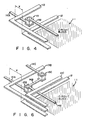
- Fig. 4 illustrates double-layered wirings
- Fig. 6 three-layered wirings.
- Signal wirings 14A and 14B need to be coupled together through via contact section 15.
- these signal wirings 14A and 14B deal only with a minute current and can be made sufficiently narrower than power wirings 12 and 13, so that via contact section 15 can be made smaller accordingly.
- the structure shown in Fig. 3 can improve the overall integration density of an IC chip, as compared with the structure shown in Fig. 1.
- the above signal wiring 14A extends to run across power wiring 13 constituted by the second aluminum layer and signal wiring 14B constituted by the second aluminum layer is provided running across power wiring 12 that is constituted by the first aluminum layer.
- Signal wirings 14B and 14A are coupled together through via contact section 15 in region Y in circuit block 11A, and signal wirings 14A and 14B are coupled through another via contact section 15 in region X in the other circuit block 11B. If the positions where signal wirings 14A and 14B are provided are set in advance in such a way as to be aligned between both circuit blocks, power wirings 12 and 13 and signal wirings 14A and 14B can be easily constituted.
- Fig. 8 is a plan pattern diagram illustrating the structure of another applied example of this invention.
- part of power wiring 12 and part of power wiring 13 are commonly provided between two adjacent circuit blocks 11C and 11D so as to make power wirings 12 and 13 at this region twice as wide as the remaining portions of these wirings.
- This structure permits a larger source current to be supplied to the circuit blocks with a high efficiency or with less power loss.
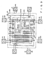
- Fig. 9 is a plan pattern diagram illustrating the structure of the overall chip of a practical semicustomized IC embodying this invention.
- This IC chip incluives, for example, two circuit blocks of specific function 11 and a basic cell region 22 consisting of a plurality of basic cell blocks 21.
- a VDD wiring 23 and a VSS wiring 24, both constituted by the second aluminum layer, run around the chip, and are coupled to a plurality of power source pads 25 constituted by the second aluminum layer through wirings that are constituted by either the first or second aluminum layer.
- Power wirings 12 and 13 each with a double-layered structure, which run around the two circuit blocks 11, are coupled to VDD wiring 23 and/or VSS wiring 24 through a wiring constituted by the first aluminum layer.
- Numeral 15 in Fig. 9, like the one in Fig. 5, is a via contact section for coupling the first and second aluminum layers.
- wirings (14A and 14B in Fig. 3) constituted by the second aluminum layer generally run in the lateral direction in Fig. 9.
- Signal wirings 14A and 14B and pads 25 for these wirings are omitted in Fig. 9 for diagrammatic simplicity.
- this invention can provide a semiconductor integrated circuit which can prevent reduction in current capacity of power wirings or the like due to the use of via contacts and does not deteriorate the chip integration density.
Landscapes
- Semiconductor Integrated Circuits (AREA)
- Design And Manufacture Of Integrated Circuits (AREA)
- Internal Circuitry In Semiconductor Integrated Circuit Devices (AREA)
Applications Claiming Priority (2)
| Application Number | Priority Date | Filing Date | Title |
|---|---|---|---|
| JP216710/87 | 1987-08-31 | ||
| JP62216710A JPH073840B2 (ja) | 1987-08-31 | 1987-08-31 | 半導体集積回路 |
Publications (2)
| Publication Number | Publication Date |
|---|---|
| EP0307722A1 true EP0307722A1 (de) | 1989-03-22 |
| EP0307722B1 EP0307722B1 (de) | 1993-03-17 |
Family
ID=16692707
Family Applications (1)
| Application Number | Title | Priority Date | Filing Date |
|---|---|---|---|
| EP88114229A Expired - Lifetime EP0307722B1 (de) | 1987-08-31 | 1988-08-31 | Halbleiteranordnung mit Mehrschichtleiter |
Country Status (5)
| Country | Link |
|---|---|
| US (1) | US4924290A (de) |
| EP (1) | EP0307722B1 (de) |
| JP (1) | JPH073840B2 (de) |
| KR (1) | KR910003544B1 (de) |
| DE (1) | DE3879333T2 (de) |
Cited By (6)
| Publication number | Priority date | Publication date | Assignee | Title |
|---|---|---|---|---|
| DE4006282A1 (de) * | 1989-02-28 | 1990-08-30 | Toshiba Kawasaki Kk | Hochgeschwindigkeitssignaluebertragungsleitungs -streckenaufbau fuer integrierte halbleiterschaltkreisanordnungen |
| EP0378809A3 (de) * | 1988-12-16 | 1990-12-12 | Kabushiki Kaisha Toshiba | Halbleiteranordnung mit einer Mehrschicht-Verbindungsstruktur |
| EP0360507A3 (de) * | 1988-09-19 | 1991-05-08 | Fujitsu Limited | Integrierte Schaltungshalbleiteranordnung mit verbesserter Einrichtung für Speiseleitungen |
| DE4102718A1 (de) * | 1990-01-30 | 1991-08-08 | Hitachi Ltd | Integrierte schaltung mit spannungsversorgungsleitung und verfahren zum layout von spannungsversorgungsleitungen |
| US5185650A (en) * | 1989-02-28 | 1993-02-09 | Kabushiki Kaisha Toshiba | High-speed signal transmission line path structure for semiconductor integrated circuit devices |
| EP0701282A3 (de) * | 1994-08-01 | 1996-10-30 | Motorola Inc | Verbindungsstruktur mit reduzierter lokaler Spitzenstromdichte und Verfahren zum Herstellen einer Verbindungsschicht in einem Halbleiterbauelement |
Families Citing this family (14)
| Publication number | Priority date | Publication date | Assignee | Title |
|---|---|---|---|---|
| JPH02106968A (ja) * | 1988-10-17 | 1990-04-19 | Hitachi Ltd | 半導体集積回路装置及びその形成方法 |
| JP2720481B2 (ja) * | 1988-10-24 | 1998-03-04 | 三菱電機株式会社 | 半導体装置 |
| US5206529A (en) * | 1989-09-25 | 1993-04-27 | Nec Corporation | Semiconductor integrated circuit device |
| JPH0410624A (ja) * | 1990-04-27 | 1992-01-14 | Hitachi Ltd | 半導体集積回路 |
| US5063429A (en) * | 1990-09-17 | 1991-11-05 | Ncr Corporation | High density input/output cell arrangement for integrated circuits |
| JP3238395B2 (ja) * | 1990-09-28 | 2001-12-10 | 株式会社東芝 | 半導体集積回路 |
| JP3030991B2 (ja) * | 1991-11-14 | 2000-04-10 | 日本電気株式会社 | 半導体集積回路 |
| US5606203A (en) * | 1993-01-20 | 1997-02-25 | Kabushiki Kaisha Toshiba | Semiconductor device having Al-Cu wiring lines where Cu concentration is related to line width |
| US5723908A (en) * | 1993-03-11 | 1998-03-03 | Kabushiki Kaisha Toshiba | Multilayer wiring structure |
| WO1995017007A1 (en) * | 1993-12-14 | 1995-06-22 | Oki America, Inc. | Efficient routing method and resulting structure for integrated circuits |
| DE4343983C2 (de) | 1993-12-22 | 1996-09-05 | Siemens Ag | Integrierte Halbleiterschaltung mit Kondensatoren genau definierter Kapazität und Verfahren zur Herstellung einer solchen Schaltung |
| JPH08306774A (ja) * | 1995-05-01 | 1996-11-22 | Oki Electric Ind Co Ltd | 半導体装置及びその製造方法 |
| JP3790202B2 (ja) | 2002-09-24 | 2006-06-28 | 松下電器産業株式会社 | 半導体集積回路の電源配線方法および半導体集積回路 |
| WO2006018891A1 (ja) * | 2004-08-20 | 2006-02-23 | Fujitsu Limited | 半導体装置及びその設計方法 |
Citations (1)
| Publication number | Priority date | Publication date | Assignee | Title |
|---|---|---|---|---|
| GB2137413A (en) * | 1983-03-11 | 1984-10-03 | Rca Corp | Variable geometry automated universal array |
Family Cites Families (8)
| Publication number | Priority date | Publication date | Assignee | Title |
|---|---|---|---|---|
| US4453176A (en) * | 1981-12-31 | 1984-06-05 | International Business Machines Corporation | LSI Chip carrier with buried repairable capacitor with low inductance leads |
| JPS59135747A (ja) * | 1983-01-24 | 1984-08-04 | Mitsubishi Electric Corp | 大規模集積回路装置 |
| JPS6030152A (ja) * | 1983-07-28 | 1985-02-15 | Toshiba Corp | 集積回路 |
| JPS60101951A (ja) * | 1983-11-08 | 1985-06-06 | Sanyo Electric Co Ltd | ゲ−トアレイ |
| DE3579344D1 (de) * | 1984-03-29 | 1990-10-04 | Sanyo Electric Co | Integrierter halbleiter-schaltkreis mit mehrschichtigen verbindungen. |
| JPS61100955A (ja) * | 1984-10-22 | 1986-05-19 | Nec Corp | 半導体装置 |
| JPH0644593B2 (ja) * | 1984-11-09 | 1994-06-08 | 株式会社東芝 | 半導体集積回路装置 |
| JPS6235643A (ja) * | 1985-08-09 | 1987-02-16 | Hitachi Ltd | 半導体集積回路装置 |
-
1987
- 1987-08-31 JP JP62216710A patent/JPH073840B2/ja not_active Expired - Lifetime
-
1988
- 1988-08-30 US US07/238,122 patent/US4924290A/en not_active Expired - Lifetime
- 1988-08-31 EP EP88114229A patent/EP0307722B1/de not_active Expired - Lifetime
- 1988-08-31 DE DE8888114229T patent/DE3879333T2/de not_active Expired - Lifetime
- 1988-08-31 KR KR1019880011134A patent/KR910003544B1/ko not_active Expired
Patent Citations (1)
| Publication number | Priority date | Publication date | Assignee | Title |
|---|---|---|---|---|
| GB2137413A (en) * | 1983-03-11 | 1984-10-03 | Rca Corp | Variable geometry automated universal array |
Non-Patent Citations (2)
| Title |
|---|
| PROCEEDINGS OF THE FIRST INTERNATIONAL IEEE VLSI MULTILEVEL INTERCONNECTION CONFERENCE, New Orleans, LA, 21st-22nd June 1984, pages 290-297, IEEE; A. FELLER et al.: "A 1.25-micron CMOS-SOS DLM optimized standard cell technology" * |
| REVIEW OF THE ELECTRICAL COMMUNICATION LABORATORIES, vol. 26, no. 9/10, September/October 1978, pages 1355-1366; K. WADA et al.: "Master-slice layout design for emitter coupled logic LSI" * |
Cited By (9)
| Publication number | Priority date | Publication date | Assignee | Title |
|---|---|---|---|---|
| EP0360507A3 (de) * | 1988-09-19 | 1991-05-08 | Fujitsu Limited | Integrierte Schaltungshalbleiteranordnung mit verbesserter Einrichtung für Speiseleitungen |
| EP0378809A3 (de) * | 1988-12-16 | 1990-12-12 | Kabushiki Kaisha Toshiba | Halbleiteranordnung mit einer Mehrschicht-Verbindungsstruktur |
| US5148263A (en) * | 1988-12-16 | 1992-09-15 | Kabushiki Kaisha Toshiba | Semiconductor device having a multi-layer interconnect structure |
| DE4006282A1 (de) * | 1989-02-28 | 1990-08-30 | Toshiba Kawasaki Kk | Hochgeschwindigkeitssignaluebertragungsleitungs -streckenaufbau fuer integrierte halbleiterschaltkreisanordnungen |
| US5185650A (en) * | 1989-02-28 | 1993-02-09 | Kabushiki Kaisha Toshiba | High-speed signal transmission line path structure for semiconductor integrated circuit devices |
| DE4102718A1 (de) * | 1990-01-30 | 1991-08-08 | Hitachi Ltd | Integrierte schaltung mit spannungsversorgungsleitung und verfahren zum layout von spannungsversorgungsleitungen |
| US5391900A (en) * | 1990-01-30 | 1995-02-21 | Hitachi, Ltd. | Integrated circuit having power trunk line and method for layout of power trunk line |
| EP0701282A3 (de) * | 1994-08-01 | 1996-10-30 | Motorola Inc | Verbindungsstruktur mit reduzierter lokaler Spitzenstromdichte und Verfahren zum Herstellen einer Verbindungsschicht in einem Halbleiterbauelement |
| US5760476A (en) * | 1994-08-01 | 1998-06-02 | Motorola, Inc. | Interconnect run between a first point and a second point in a semiconductor device for reducing electromigration failure |
Also Published As
| Publication number | Publication date |
|---|---|
| JPS6459831A (en) | 1989-03-07 |
| KR910003544B1 (ko) | 1991-06-04 |
| DE3879333D1 (de) | 1993-04-22 |
| EP0307722B1 (de) | 1993-03-17 |
| DE3879333T2 (de) | 1993-06-24 |
| JPH073840B2 (ja) | 1995-01-18 |
| KR890004432A (ko) | 1989-04-22 |
| US4924290A (en) | 1990-05-08 |
Similar Documents
| Publication | Publication Date | Title |
|---|---|---|
| US4924290A (en) | Semiconductor device having improved multilayered wirings | |
| US5101261A (en) | Electronic circuit device with electronomigration-resistant metal conductors | |
| US5045725A (en) | Integrated standard cell including clock lines | |
| JP3179800B2 (ja) | 半導体集積回路装置 | |
| US5672909A (en) | Interdigitated wirebond programmable fixed voltage planes | |
| US20030183935A1 (en) | Capacitor for signal propagation across ground plane boundaries in superconductor integrated circuits | |
| JPH0587977B2 (de) | ||
| WO2005045929A1 (en) | Integrated circuit bond pad structures and methods of making | |
| CN101009256A (zh) | 半导体装置 | |
| KR100384745B1 (ko) | 반도체집적회로장치 | |
| US6111310A (en) | Radially-increasing core power bus grid architecture | |
| JP4932980B2 (ja) | オン・ダイ型のデカップリング・キャパシタンスを有する半導体ダイ | |
| JP3473516B2 (ja) | 半導体集積回路 | |
| EP0394878B1 (de) | Halbleiteranordnung mit Mehrschichtleiterstruktur | |
| TWI252560B (en) | Integrated circuit design for routing an electrical connection | |
| EP0703617A2 (de) | Monolitische integrierte Schaltung höher Frequenz | |
| US6730985B2 (en) | Semiconductor integrated circuit device | |
| US20040226735A1 (en) | Method and apparatus for integrated noise decoupling | |
| JPH08274127A (ja) | 半導体装置 | |
| JPH01239964A (ja) | 半導体集積回路の電源配線レイアウト法 | |
| EP0335965A1 (de) | Phantom-esd-schutzschaltung mit e-feldverdichtung | |
| EP0558984A2 (de) | Keramische Hybrid-Modulstruktur vom Dünnschicht-Typ | |
| JP3075858B2 (ja) | 半導体集積回路装置 | |
| JP2551499B2 (ja) | 半導体集積回路装置 | |
| Mezhiba et al. | Variation of inductance with frequency in high performance power distribution grids [ICs] |
Legal Events
| Date | Code | Title | Description |
|---|---|---|---|
| PUAI | Public reference made under article 153(3) epc to a published international application that has entered the european phase |
Free format text: ORIGINAL CODE: 0009012 |
|
| 17P | Request for examination filed |
Effective date: 19880927 |
|
| AK | Designated contracting states |
Kind code of ref document: A1 Designated state(s): DE FR GB |
|
| RIN1 | Information on inventor provided before grant (corrected) |
Inventor name: KATO, TOSHIYA Inventor name: ENKAKU, MOTOHIRO C/O PATENT DIVISION |
|
| 17Q | First examination report despatched |
Effective date: 19901203 |
|
| GRAA | (expected) grant |
Free format text: ORIGINAL CODE: 0009210 |
|
| AK | Designated contracting states |
Kind code of ref document: B1 Designated state(s): DE FR GB |
|
| REF | Corresponds to: |
Ref document number: 3879333 Country of ref document: DE Date of ref document: 19930422 |
|
| ET | Fr: translation filed | ||
| PLBE | No opposition filed within time limit |
Free format text: ORIGINAL CODE: 0009261 |
|
| STAA | Information on the status of an ep patent application or granted ep patent |
Free format text: STATUS: NO OPPOSITION FILED WITHIN TIME LIMIT |
|
| 26N | No opposition filed | ||
| PGFP | Annual fee paid to national office [announced via postgrant information from national office to epo] |
Ref country code: FR Payment date: 19970811 Year of fee payment: 10 |
|
| PGFP | Annual fee paid to national office [announced via postgrant information from national office to epo] |
Ref country code: GB Payment date: 19970822 Year of fee payment: 10 |
|
| PG25 | Lapsed in a contracting state [announced via postgrant information from national office to epo] |
Ref country code: GB Free format text: LAPSE BECAUSE OF NON-PAYMENT OF DUE FEES Effective date: 19980831 |
|
| GBPC | Gb: european patent ceased through non-payment of renewal fee |
Effective date: 19980831 |
|
| PG25 | Lapsed in a contracting state [announced via postgrant information from national office to epo] |
Ref country code: FR Free format text: LAPSE BECAUSE OF NON-PAYMENT OF DUE FEES Effective date: 19990430 |
|
| REG | Reference to a national code |
Ref country code: FR Ref legal event code: ST |
|
| PGFP | Annual fee paid to national office [announced via postgrant information from national office to epo] |
Ref country code: DE Payment date: 20070823 Year of fee payment: 20 |