EP0307773A1 - Verfahren zur Herstellung elektronischer Module, insbesondere für Informationskarten - Google Patents
Verfahren zur Herstellung elektronischer Module, insbesondere für Informationskarten Download PDFInfo
- Publication number
- EP0307773A1 EP0307773A1 EP88114579A EP88114579A EP0307773A1 EP 0307773 A1 EP0307773 A1 EP 0307773A1 EP 88114579 A EP88114579 A EP 88114579A EP 88114579 A EP88114579 A EP 88114579A EP 0307773 A1 EP0307773 A1 EP 0307773A1
- Authority
- EP
- European Patent Office
- Prior art keywords
- unit
- chip
- electrodes
- substrate
- conductors
- Prior art date
- Legal status (The legal status is an assumption and is not a legal conclusion. Google has not performed a legal analysis and makes no representation as to the accuracy of the status listed.)
- Granted
Links
Images


Classifications
-
- G—PHYSICS
- G06—COMPUTING OR CALCULATING; COUNTING
- G06K—GRAPHICAL DATA READING; PRESENTATION OF DATA; RECORD CARRIERS; HANDLING RECORD CARRIERS
- G06K19/00—Record carriers for use with machines and with at least a part designed to carry digital markings
- G06K19/06—Record carriers for use with machines and with at least a part designed to carry digital markings characterised by the kind of the digital marking, e.g. shape, nature, code
- G06K19/067—Record carriers with conductive marks, printed circuits or semiconductor circuit elements, e.g. credit or identity cards also with resonating or responding marks without active components
- G06K19/07—Record carriers with conductive marks, printed circuits or semiconductor circuit elements, e.g. credit or identity cards also with resonating or responding marks without active components with integrated circuit chips
- G06K19/077—Constructional details, e.g. mounting of circuits in the carrier
- G06K19/07745—Mounting details of integrated circuit chips
- G06K19/07747—Mounting details of integrated circuit chips at least one of the integrated circuit chips being mounted as a module
-
- G—PHYSICS
- G06—COMPUTING OR CALCULATING; COUNTING
- G06K—GRAPHICAL DATA READING; PRESENTATION OF DATA; RECORD CARRIERS; HANDLING RECORD CARRIERS
- G06K19/00—Record carriers for use with machines and with at least a part designed to carry digital markings
- G06K19/06—Record carriers for use with machines and with at least a part designed to carry digital markings characterised by the kind of the digital marking, e.g. shape, nature, code
- G06K19/067—Record carriers with conductive marks, printed circuits or semiconductor circuit elements, e.g. credit or identity cards also with resonating or responding marks without active components
- G06K19/07—Record carriers with conductive marks, printed circuits or semiconductor circuit elements, e.g. credit or identity cards also with resonating or responding marks without active components with integrated circuit chips
- G06K19/077—Constructional details, e.g. mounting of circuits in the carrier
- G06K19/07743—External electrical contacts
-
- G—PHYSICS
- G06—COMPUTING OR CALCULATING; COUNTING
- G06K—GRAPHICAL DATA READING; PRESENTATION OF DATA; RECORD CARRIERS; HANDLING RECORD CARRIERS
- G06K19/00—Record carriers for use with machines and with at least a part designed to carry digital markings
- G06K19/06—Record carriers for use with machines and with at least a part designed to carry digital markings characterised by the kind of the digital marking, e.g. shape, nature, code
- G06K19/067—Record carriers with conductive marks, printed circuits or semiconductor circuit elements, e.g. credit or identity cards also with resonating or responding marks without active components
- G06K19/07—Record carriers with conductive marks, printed circuits or semiconductor circuit elements, e.g. credit or identity cards also with resonating or responding marks without active components with integrated circuit chips
- G06K19/077—Constructional details, e.g. mounting of circuits in the carrier
- G06K19/07745—Mounting details of integrated circuit chips
-
- H—ELECTRICITY
- H10—SEMICONDUCTOR DEVICES; ELECTRIC SOLID-STATE DEVICES NOT OTHERWISE PROVIDED FOR
- H10W—GENERIC PACKAGES, INTERCONNECTIONS, CONNECTORS OR OTHER CONSTRUCTIONAL DETAILS OF DEVICES COVERED BY CLASS H10
- H10W70/00—Package substrates; Interposers; Redistribution layers [RDL]
- H10W70/60—Insulating or insulated package substrates; Interposers; Redistribution layers
- H10W70/699—Insulating or insulated package substrates; Interposers; Redistribution layers for flat cards, e.g. credit cards
-
- H—ELECTRICITY
- H05—ELECTRIC TECHNIQUES NOT OTHERWISE PROVIDED FOR
- H05K—PRINTED CIRCUITS; CASINGS OR CONSTRUCTIONAL DETAILS OF ELECTRIC APPARATUS; MANUFACTURE OF ASSEMBLAGES OF ELECTRICAL COMPONENTS
- H05K1/00—Printed circuits
- H05K1/02—Details
- H05K1/11—Printed elements for providing electric connections to or between printed circuits
- H05K1/111—Pads for surface mounting, e.g. lay-out
- H05K1/112—Pads for surface mounting, e.g. lay-out directly combined with via connections
-
- H—ELECTRICITY
- H05—ELECTRIC TECHNIQUES NOT OTHERWISE PROVIDED FOR
- H05K—PRINTED CIRCUITS; CASINGS OR CONSTRUCTIONAL DETAILS OF ELECTRIC APPARATUS; MANUFACTURE OF ASSEMBLAGES OF ELECTRICAL COMPONENTS
- H05K3/00—Apparatus or processes for manufacturing printed circuits
- H05K3/30—Assembling printed circuits with electric components, e.g. with resistors
- H05K3/32—Assembling printed circuits with electric components, e.g. with resistors electrically connecting electric components or wires to printed circuits
- H05K3/34—Assembling printed circuits with electric components, e.g. with resistors electrically connecting electric components or wires to printed circuits by soldering
- H05K3/341—Surface mounted components
- H05K3/3421—Leaded components
-
- Y—GENERAL TAGGING OF NEW TECHNOLOGICAL DEVELOPMENTS; GENERAL TAGGING OF CROSS-SECTIONAL TECHNOLOGIES SPANNING OVER SEVERAL SECTIONS OF THE IPC; TECHNICAL SUBJECTS COVERED BY FORMER USPC CROSS-REFERENCE ART COLLECTIONS [XRACs] AND DIGESTS
- Y10—TECHNICAL SUBJECTS COVERED BY FORMER USPC
- Y10T—TECHNICAL SUBJECTS COVERED BY FORMER US CLASSIFICATION
- Y10T29/00—Metal working
- Y10T29/49—Method of mechanical manufacture
- Y10T29/49002—Electrical device making
- Y10T29/49117—Conductor or circuit manufacturing
- Y10T29/49121—Beam lead frame or beam lead device
-
- Y—GENERAL TAGGING OF NEW TECHNOLOGICAL DEVELOPMENTS; GENERAL TAGGING OF CROSS-SECTIONAL TECHNOLOGIES SPANNING OVER SEVERAL SECTIONS OF THE IPC; TECHNICAL SUBJECTS COVERED BY FORMER USPC CROSS-REFERENCE ART COLLECTIONS [XRACs] AND DIGESTS
- Y10—TECHNICAL SUBJECTS COVERED BY FORMER USPC
- Y10T—TECHNICAL SUBJECTS COVERED BY FORMER US CLASSIFICATION
- Y10T29/00—Metal working
- Y10T29/49—Method of mechanical manufacture
- Y10T29/49002—Electrical device making
- Y10T29/49117—Conductor or circuit manufacturing
- Y10T29/49124—On flat or curved insulated base, e.g., printed circuit, etc.
- Y10T29/4913—Assembling to base an electrical component, e.g., capacitor, etc.
- Y10T29/49144—Assembling to base an electrical component, e.g., capacitor, etc. by metal fusion
Definitions
- the present invention relates to a method for manufacturing an electronic module, in particular for a microcircuit card, this module comprising a plurality of electrodes intended to come into contact with an apparatus into which the card is inserted, at least one integrated circuit chip. having a front face provided with connection terminals and a rear face, and a set of conductors connecting said electrodes to the connection terminals of the chip.
- electronic modules intended to equip transaction cards are generally in the form of a patch intended to be incorporated in a corresponding opening of the card body located in a corner thereof and comprising a memory and a microprocessor integrated in the form of a single chip or two chips connected together by electrical conductors, a set of contact pads, often eight in number, connected only to the microprocessor and an insulating body in which are embedded all the other elements except, of course, for the conductive pads or electrodes which must remain accessible for the connection parts of a device, for example a computer terminal, into which the card is intended to be inserted.
- this insulating body which defines the shape of the patch and which protects the elements which it surrounds is composed of a support part and a cover part, in others it is a homogeneous coating.
- a microcircuit payment card must have the same format as a conventional magnetic stripe card. standardized whose length is 85 mm, the width of 54 mm and the thickness of 0.76 mm (ISO standards) or at least of the neighboring dimensions to remain compact and easily maneuverable.
- a thickness of 760 microns roughly corresponds only to twice that of an unprotected integrated circuit chip
- the portion of the surface of the card that can be allocated to the electronic unit is very limited since most of it must be reserved for registrations such as the name of the service provider issuing the card, the identity of the holder, a signature, usage information and possibly a photo and that, thirdly, the conductive areas must be large enough for contact with the connection parts of a device to be ensured and good, it can be deduced very quickly that it is not possible to use standardized circuits already coated or encased like those currently found on the market and which are too bulky.
- the cards must be able to be produced in large series and at a very low cost price, especially if they are cards to which is initially attributed a certain value which one pays by buying them and which, when this value is exhausted, should simply be discarded.
- the conductive pads or electrodes are also subject to standards as to their positions on the map, the minimum size that their surfaces must have and finally the functions assigned to them. On this subject, we will consult with profit the draft ISO standard n ° 7816 / 2.2 established by the TC 97 technical committee. document are assigned to the eight designated electrodes from C1 to C8 specific functions, for example at electrode C1 the supply voltage VCC, at electrode C3 the clock signal CLK, at electrode C5 ground GND and at the electrode C7 the input and output data I / O. It will be understood that this order will not necessarily correspond to that which has been chosen for the chip to be used, so that it may be a question of considering detours of conductors connecting said electrodes to the connection terminals of the chip. At least one embodiment of the electronic module according to the present invention should allow these detours to adapt a chip having connection terminals arranged in any order, to electrodes of a standardized electronic module.
- the module described in document DE-A-3 248 385 is composed of two units.
- the first unit comprises a first substrate on which electrodes are printed on its visible face, the opposite face of the substrate carrying metallizations connected to the electrodes by metallized holes.
- the second unit comprises a second substrate and metallized conductors intended to connect the terminals of a chip to the metallizations carried by the first substrate. Under each of these conductors is pierced an opening through which it is possible to solder the conductor to the corresponding metallization of the first substrate.
- the present invention provides printed conductors which have ends capable of being folded in such a way that they can be introduced into holes giving access to the electrodes of the module, then welded to these electrodes.
- the object of the invention is to provide a satisfactory solution to the various problems which have been mentioned above.
- the method of manufacturing the electronic module is characterized in that: a first unit is manufactured comprising an insulating substrate which carries a plurality of electrodes, each electrode covering a hole made in said substrate, - a second unit is manufactured by following the following operations: one is provided with an integrated circuit chip and an insulating substrate, the substrate is coated with adhesive material, a rectangular opening is made in the substrate whose dimensions are slightly larger than the peripheral dimensions of the chip, the substrate is perforated with a number of second holes corresponding to the number of first holes made in the first unit, said second holes being arranged to be substantially coaxial with the first when said first and second units are superimposed, a metal sheet is applied to said adhesive material, said sheet is chemically etched to form a network of conductors such that one of the first free ends of each of said conductors falls in line with a connection terminal of the chip and that each of the second free ends of each of said conductors falls in line with a corresponding second hole of the second unit, the front face of
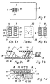
- FIG. 1 shows a plan view of a microcircuit card comprising an electronic module 1 inserted in a support 2.
- the support 2 is standardized as regards its dimensions.
- the electronic module generally comprises eight electrodes 7 whose dimensions, locations relative to the edges of the card and the functions are also standardized. Each electrode 7 is a rectangle whose minimum dimensions are 2.0 x 1.7 mm.
- the integrated circuit chip 10 is placed between the electrodes 7 and under the insulating substrate which carries said electrodes. The electrodes are intended to come into electrical contact with a device into which the card is inserted.
- a set of conductors, not shown in FIG. 1, but which will be described below connect the electrodes to the connection terminals of the chip.
- the present invention describes a way of producing the electronic module 1, a possible way of placing the module in the support 2 being mentioned at the end of this description only to make the latter more complete.
- first unit as shown in perspective in Figure 2a.
- This first unit comprises an insulating substrate 6 covered by a plurality of electrodes 7, the surface of which covers at least the standardized area discussed in connection with FIG. 1.
- Each electrode 7 first covers a hole 8 made in the substrate 6.
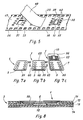
- FIGS. 3a and 3b A first manufacturing method is shown in FIGS. 3a and 3b which uses a film for mass production. It could however be a production piece by piece in which case there would be as many substrates as pieces.
- a film with an insulating support 20 as shown in Figure 3a, made of polyimide, polyester or glass-epoxy (thickness of the order of 125 microns).
- the substrate 20 is coated with an adhesive material 22, the thickness of which can vary between 25 and 35 ⁇ m.
- the substrate thus coated is then perforated with a number of holes 8 corresponding to the number of electrodes 7 that the first unit 5 will carry (see FIG. 2a) once produced.
- a metallic sheet 21 (thickness between 35 and 70 ⁇ m) is then applied by laminating it to the substrate 20 which adheres strongly to it because of the adhesive layer 22.
- the said sheet is chemically etched according to a process similar to that used for make them printed circuits so as to obtain the field of electrodes 7 by arranging so that each electrode 7 covers a hole.
- FIG. 3a shows a 35 mm film with standardized perforations 23.
- the electrodes 7 it will be possible to accommodate two first units across the width of the film, while the figure shows only one, simply to do well show details of the manufacturing process.
- FIGS. 4a to 4c a second way of manufacturing this first unit can be implemented, which will now be explained, illustrated by FIGS. 4a to 4c.
- a metal foil is provided 25.
- the electrodes 7 are formed by stamping or by chemical etching as shown in FIG. 4a, the electrodes being separated from each other by partitions 26, but remaining connected to the sheet by bridges 27 to keep everything together. It also provides an insulating substrate 28 which is coated with adhesive material 22 ( Figure 4b). The substrate thus covered is then perforated with a number of holes 8 corresponding to the number of electrodes 7 carried by the first unit 5 at the end of its manufacture. We then apply the sheet 25 ( Figure 4a) on the substrate 28 ( Figure 4b) by arranging so that each electrode 7 comes to cover a corresponding hole 8. Finally we stamp the assembly thus formed by arranging to cut the bridges 27 at the same time. We then obtain the first unit 5 shown in Figure 4c.
- the first unit thus obtained can also be produced in large series on standardized films, as described with reference to FIG. 3b.
- a second unit 35 is then manufactured, the final appearance of which is shown in perspective in FIG. 2b.
- This second unit comprises an insulating support 36 in which a rectangular opening 37 is made, the dimensions of which are slightly larger than the peripheral dimensions of an integrated circuit chip 10 which takes place in said opening 37.
- the support 36 is still pierced with 'A plurality of second holes 38 corresponding to the first holes 8 made in the first unit 5, these second holes being arranged to be substantially coaxial with the first when the first and second units are superimposed.
- This coincidence of construction is shown in the drawing by two lines 16 and 17.
- the insulating support or substrate 36 also carries a plurality of conductors 39, the first free ends 40 of each of these conductors falling in line with a connection terminal of the chip (not shown in FIG.
- the chip 10 which, for its part, has a front face 11 provided with connection terminals and a rear face 12 which is devoid of it, is introduced into the opening 37 and its connection terminals are soldered to the first free ends 40 of the conductors 39.
- each of the conductors 39 of the second unit 35 is introduced, by its second end 41, into a corresponding hole 8 in the first unit 5 and each of these ends 41 is welded to a corresponding electrode 7.
- FIG. 2d shows on an enlarged scale the zone B delimited in dotted lines in FIG. 2c.
- the first unit 5 with its substrate 6 and an electrode 7 between which there is an adhesive layer 22.
- the first hole 8 enters the second end 41 of conductor 39. This end is welded to the electrode 7.
- the first end 40 of conductor 39 is welded to a connection terminal 42 of the front face 11 of the chip 10.
- FIG. 2d also shows that the free space 43 formed between the peripheral edge of the chip 10 and the restangular opening 37 into which this chip is inserted, as well as the space 44 formed between the conductors 39 and the front face of the chip is filled with a resinous mass 45 applied to stiffen together the chip 10, the substrate 36 and the conductors 39.
- the same figure also shows an extremely thin layer of glue 46 used to bond the first unit 5 to the second unit 35 In reality the majority of the glue will be located between the conductors 39 at a location not visible in the drawing, and these conductors will be given a shape which will force the glue to slide there when applying the two units against each other, this in order to minimize the thickness taken by the glue.
- FIG. 2d finally shows a layer of glue 47 which results from the manufacture of the second unit.
- insulating substrate 36 which is here in the form of a standardized 35 mm film.
- the substrate is coated with adhesive material 47.
- the substrate is perforated with the restangular opening 37 and second holes 38.
- a metal sheet 48 is applied to the adhesive material.
- the conductors 39 are shown by photolithographic process.
- the second unit is made of film, which is the case shown in Figure 5, we cut this second unit of film to obtain the part 35 shown in FIG. 2b.
- the network of conductors 39 being supported by an insulating substrate 36, an adhesive film 47 being interposed between each conductor and the substrate, the product illustrated in FIG. 2b is given the name of three-layer film.
- FIG. 5 shows a 35 mm film with standard perforations 23.
- this kind of film it will generally be possible to accommodate two second units in the width of this film, while the figure shows only one, this simply for clearly show the detail of the manufacturing process.
- FIGS. 6a and 6b show, seen from above, respectively a practical embodiment of a first unit 5 and of a second unit 35 before their assembly and produced according to the invention.
- the electrodes 7 of the unit 5 are identified by the references C1 to C8 according to the ISO standard mentioned in the introduction to this description. These electrodes are at least equal in area to the standard area; each covers a first hole 8.
- FIG. 6a shows that the zone 50 situated between the electrodes, as well as between the two rows of electrodes, is made of the same metal which said electrodes, a space 51 without metal being provided to insulate these electrodes of said zone 50.
- This zone 50 is electrically connected to the electrode C5 by an isthmus 52. This is intentionally sought since the electrode C5 represents the mass (GND) of the chip which, by this isthmus, achieves a shielding for the chip.
- GND mass
- the second unit 35 shown in FIG. 6b has an external cutout identical to the external cutout of the first unit 5. Once superimposed, the two units have only one edge (see also FIG. 7a).
- the second unit 35 is equipped with a chip 10 whose functions of the output terminals are not ordered in the same way as those of the standard electrodes of the module. It is therefore necessary to operate certain detours of conductors 39, detours which are visible in FIG. 6b (for example conductors 53, 54, and 55).
- the invention has the advantage of enabling these detours by means of which a chip can be used, the terminals of which are arranged in any way to equip an electronic module, the electrodes of which are standardized.
- FIGS 7a, 7b and 7c show in perspective three completed electronic modules made according to the invention.
- the electronic module 1 in FIG. 7a is composed of the first unit 5 and the second unit 35. Although this is not visible in the drawing, the chip of the unit 35 is placed between two rows of second holes (as shown in Figure 2c).
- Figure 7a shows that once superimposed, the units 5 and 35 are edge to edge, which implies that the first and second units have the same surfaces and the same contours. In this case, a housing of the same shape and thickness as the module in the microcircuit card will be provided and the module will be stuck in the card in the same way as a stamp on a letter.
- FIG. 7b shows how such a module can be inserted in a map if one establishes a section along the line VIII-VIII in Figure 7b.
- the module 1 of Figure 2c with its first and second units.
- the card 2 consists of a superposition of layers pressed together and referenced 71, 72, 73 and 74.
- the layer 71 surrounds the first unit and its insulating substrate 6 and the layer 72 surrounds the insulating substrate 36 of the second unit.
- the layer 73 extends to the periphery of the chip 10, while the layer 74 forms a closing layer.
- the film generally 35 mm perforated in a standard manner, is used to implement a well known system, TAB (tape automated bonding) which will be usefully used in the present invention to produce the first and second units necessary for the production of the electronic module of the invention.
- TAB tape automated bonding
- first and second units are manufactured separately on their respective supports. Instead of detaching each of the units from its support just before assembly, one could detach only the first unit from its support, which is then assembled on a second unit which remains attached to its support.
- the modules are then delivered in strips to the inserter who is responsible for cutting them up and mounting them in the cards. This way of doing things is elegant, quick for inserting work and does not require any special precautions, the module being well protected from itself as it emerges from this description.
- modules are delivered piece by piece or mounted on film, they will constitute a standard unit for the inserter who will no longer have to worry about the particular wishes presented by customers, these wishes having already been satisfied by the manufacturer of the electronic module.
- the first unit 5 does not comprise any drilling for the passage of the chip and that in this this unit serves as protection towards the exterior of said chip.
- the conductors 39 are located on the front face of the second unit 35 and are in contact with the rear face of the first unit, which is important for obtaining a reduced thickness of the module, on the one hand, and to facilitate the manufacture of the second unit, on the other hand.
Landscapes
- Engineering & Computer Science (AREA)
- Computer Hardware Design (AREA)
- Microelectronics & Electronic Packaging (AREA)
- Physics & Mathematics (AREA)
- General Physics & Mathematics (AREA)
- Theoretical Computer Science (AREA)
- Credit Cards Or The Like (AREA)
Priority Applications (1)
| Application Number | Priority Date | Filing Date | Title |
|---|---|---|---|
| AT88114579T ATE71770T1 (de) | 1987-09-14 | 1988-09-07 | Verfahren zur herstellung elektronischer module, insbesondere fuer informationskarten. |
Applications Claiming Priority (2)
| Application Number | Priority Date | Filing Date | Title |
|---|---|---|---|
| FR8712739A FR2620586A1 (fr) | 1987-09-14 | 1987-09-14 | Procede de fabrication de modules electroniques, notamment pour cartes a microcircuits |
| FR8712739 | 1987-09-14 |
Publications (2)
| Publication Number | Publication Date |
|---|---|
| EP0307773A1 true EP0307773A1 (de) | 1989-03-22 |
| EP0307773B1 EP0307773B1 (de) | 1992-01-15 |
Family
ID=9354898
Family Applications (1)
| Application Number | Title | Priority Date | Filing Date |
|---|---|---|---|
| EP88114579A Expired - Lifetime EP0307773B1 (de) | 1987-09-14 | 1988-09-07 | Verfahren zur Herstellung elektronischer Module, insbesondere für Informationskarten |
Country Status (6)
| Country | Link |
|---|---|
| US (1) | US4835846A (de) |
| EP (1) | EP0307773B1 (de) |
| JP (1) | JPH0199894A (de) |
| AT (1) | ATE71770T1 (de) |
| DE (1) | DE3867776D1 (de) |
| FR (1) | FR2620586A1 (de) |
Cited By (16)
| Publication number | Priority date | Publication date | Assignee | Title |
|---|---|---|---|---|
| FR2674404A1 (fr) * | 1991-03-22 | 1992-09-25 | Toshiba Kk | Dispositif a carte a circuit integre. |
| FR2674681A1 (fr) * | 1991-03-28 | 1992-10-02 | Em Microelectronic Marin Sa | Composant electronique ultramince et procede pour sa fabrication. |
| FR2684236A1 (fr) * | 1991-11-27 | 1993-05-28 | Gemplus Card Int | Dispositif de connexion de circuit integre. |
| EP0509379B1 (de) * | 1991-04-11 | 1995-11-15 | Eta SA Fabriques d'Ebauches | Elektromagnetischer Mikromotor mit Axialfluss |
| EP0688050A1 (de) * | 1994-06-15 | 1995-12-20 | Philips Cartes Et Systemes | Montageverfahren für IC-Karte und so erhaltene Karte |
| FR2726106A1 (fr) * | 1994-10-21 | 1996-04-26 | Solaic Sa | Carte electronique utilisable avec un lecteur de cartes sans contact et un lecteur de cartes a contacts |
| EP0674346A3 (de) * | 1994-03-22 | 1997-02-05 | Toshiba Kk | Anschlussstelle für Halbleiterbauelement. |
| DE19809073A1 (de) * | 1998-03-04 | 1999-09-16 | Orga Kartensysteme Gmbh | Chipmodul und Verfahren zur Herstellung einer Chipkarte |
| US6166431A (en) * | 1995-08-25 | 2000-12-26 | Kabushiki Kaisha Tishiba | Semiconductor device with a thickness of 1 MM or less |
| WO2003026010A1 (fr) * | 2001-09-18 | 2003-03-27 | Nagra Id Sa | Étiquette électronique de faible épaisseur et procédé de fabrication d'une telle étiquette |
| DE10202727A1 (de) * | 2002-01-24 | 2003-08-21 | Infineon Technologies Ag | Trägersubstrat für ein Chipmodul, Chipmodul und Chipkarte |
| EP0919950B1 (de) * | 1997-06-23 | 2007-04-04 | Rohm Co., Ltd. | Modul für ic-karte, ic-karte und verfahren zu seiner herstellung |
| FR2957175A1 (fr) * | 2010-03-08 | 2011-09-09 | Sansystems | Dispositif electronique a puce et procede de fabrication par bobines. |
| EP2608114A1 (de) * | 2011-12-19 | 2013-06-26 | Gemalto SA | Verfahren zur Herstellung eines durch ein Plättchen geschützten Chip-Moduls eines integrierten Schaltkreises |
| EP2825001A1 (de) * | 2013-07-10 | 2015-01-14 | Gemalto SA | Elektronisches Modul mit klebende dielektrische Beschichtung, und sein Herstellungsverfahren |
| WO2015003884A1 (fr) * | 2013-07-10 | 2015-01-15 | Gemalto Sa | Module electronique sans film dielectrique et son procede de fabrication |
Families Citing this family (39)
| Publication number | Priority date | Publication date | Assignee | Title |
|---|---|---|---|---|
| FR2616995A1 (fr) * | 1987-06-22 | 1988-12-23 | Ebauchesfabrik Eta Ag | Procede de fabrication de modules electroniques |
| FR2631200B1 (fr) * | 1988-05-09 | 1991-02-08 | Bull Cp8 | Circuit imprime souple, notamment pour carte a microcircuits electroniques, et carte incorporant un tel circuit |
| EP0361985B1 (de) * | 1988-09-30 | 1994-12-07 | Raychem Limited | Verbindungsartikel für Hybrid-Mikrochip |
| USRE35385E (en) * | 1988-12-12 | 1996-12-03 | Sgs-Thomson Microelectronics, Sa. | Method for fixing an electronic component and its contacts to a support |
| USRE35578E (en) * | 1988-12-12 | 1997-08-12 | Sgs-Thomson Microelectronics, Inc. | Method to install an electronic component and its electrical connections on a support, and product obtained thereby |
| US5282113A (en) * | 1990-03-05 | 1994-01-25 | Hitachi Maxell, Ltd. | Memory card with a plurality of contact spaces |
| US5049728A (en) * | 1990-04-04 | 1991-09-17 | Rovin George H | IC card system with removable IC modules |
| US5404584A (en) * | 1990-08-06 | 1995-04-04 | Ericsson Ge Mobile Communications Inc. | Printed circuit board having modularized circuit functions designed for early diagnostics |
| US5189363A (en) * | 1990-09-14 | 1993-02-23 | Ibm Corporation | Integrated circuit testing system having a cantilevered contact lead probe pattern mounted on a flexible tape for interconnecting an integrated circuit to a tester |
| US5255430A (en) * | 1992-10-08 | 1993-10-26 | Atmel Corporation | Method of assembling a module for a smart card |
| DE4344297A1 (de) * | 1993-12-23 | 1995-06-29 | Giesecke & Devrient Gmbh | Verfahren zur Herstellung von Ausweiskarten |
| DE4421607A1 (de) * | 1994-06-21 | 1996-01-04 | Giesecke & Devrient Gmbh | Verfahren zur Herstellung von Datenträgern |
| JPH09327990A (ja) * | 1996-06-11 | 1997-12-22 | Toshiba Corp | カード型記憶装置 |
| EA001552B1 (ru) * | 1996-11-20 | 2001-04-23 | Тексек, Инкорпорейтед | Криптографический носитель информации |
| DE69631829T2 (de) * | 1996-12-02 | 2005-01-13 | Swisscom Mobile Ag | IC-Karte und Program für IC-Karten |
| EP1034942A4 (de) * | 1996-12-26 | 2005-07-06 | Hitachi Ltd | Halbleiteranordnung und herstellungsverfahren dafür |
| FR2778769B1 (fr) * | 1998-05-15 | 2001-11-02 | Gemplus Sca | Carte a circuit integre comportant un bornier d'interface et procede de fabrication d'une telle carte |
| FR2781298B1 (fr) * | 1998-07-20 | 2003-01-31 | St Microelectronics Sa | Procede de fabrication d'une carte a puce electronique et carte a puce electronique |
| US6173897B1 (en) * | 1998-07-27 | 2001-01-16 | John W. Halpern | Universal card interface module for contact free cards |
| TW449796B (en) * | 2000-08-02 | 2001-08-11 | Chiou Wen Wen | Manufacturing method for integrated circuit module |
| JP2003341782A (ja) * | 2002-05-27 | 2003-12-03 | Oki Electric Ind Co Ltd | 電子デバイス収容体、電子デバイスの搬送方法、電子デバイスの実装方法、電子デバイスの収容方法 |
| EP1376462A1 (de) * | 2002-06-19 | 2004-01-02 | SCHLUMBERGER Systèmes | Verfahren zur Herstellung eines Bandes |
| FI119583B (fi) * | 2003-02-26 | 2008-12-31 | Imbera Electronics Oy | Menetelmä elektroniikkamoduulin valmistamiseksi |
| KR100651563B1 (ko) * | 2005-07-07 | 2006-11-29 | 삼성전기주식회사 | 전자부품이 내장된 배선기판의 제조방법 |
| CN103473593B (zh) * | 2012-06-05 | 2018-10-19 | 德昌电机(深圳)有限公司 | 智能卡、智能卡接触垫载板及其制造方法 |
| USD707682S1 (en) * | 2012-12-05 | 2014-06-24 | Logomotion, S.R.O. | Memory card |
| US9888283B2 (en) | 2013-03-13 | 2018-02-06 | Nagrastar Llc | Systems and methods for performing transport I/O |
| USD758372S1 (en) * | 2013-03-13 | 2016-06-07 | Nagrastar Llc | Smart card interface |
| USD759022S1 (en) * | 2013-03-13 | 2016-06-14 | Nagrastar Llc | Smart card interface |
| US9647997B2 (en) | 2013-03-13 | 2017-05-09 | Nagrastar, Llc | USB interface for performing transport I/O |
| USD729808S1 (en) * | 2013-03-13 | 2015-05-19 | Nagrastar Llc | Smart card interface |
| EP4194220A1 (de) | 2013-06-09 | 2023-06-14 | Apple Inc. | Elektronische uhr |
| USD780763S1 (en) * | 2015-03-20 | 2017-03-07 | Nagrastar Llc | Smart card interface |
| USD864968S1 (en) | 2015-04-30 | 2019-10-29 | Echostar Technologies L.L.C. | Smart card interface |
| EP3423993B1 (de) * | 2016-03-01 | 2020-07-01 | Cardlab ApS | Schaltungsschicht für eine chipkarte |
| JP1647393S (de) | 2018-02-01 | 2019-12-09 | ||
| US11200386B2 (en) * | 2018-09-27 | 2021-12-14 | Apple Inc. | Electronic card having an electronic interface |
| USD930000S1 (en) | 2018-10-12 | 2021-09-07 | Huawei Technologies Co., Ltd. | Memory card |
| TWI793030B (zh) * | 2022-06-02 | 2023-02-11 | 義隆電子股份有限公司 | 具有指紋感測器的卡片及其製造方法 |
Citations (5)
| Publication number | Priority date | Publication date | Assignee | Title |
|---|---|---|---|---|
| FR2439438A1 (fr) * | 1978-10-19 | 1980-05-16 | Cii Honeywell Bull | Ruban porteur de dispositifs de traitement de signaux electriques, son procede de fabrication et application de ce ruban a un element de traitement de signaux |
| GB2081974A (en) * | 1980-08-05 | 1982-02-24 | Gao Ges Automation Org | Carrier element for an ic module |
| DE3248385A1 (de) * | 1982-12-28 | 1984-06-28 | GAO Gesellschaft für Automation und Organisation mbH, 8000 München | Ausweiskarte mit integriertem schaltkreis |
| FR2548857A1 (fr) * | 1983-07-04 | 1985-01-11 | Cortaillod Cables Sa | Procede de fabrication en continu d'une carte imprimee |
| FR2580416A1 (fr) * | 1985-04-12 | 1986-10-17 | Radiotechnique Compelec | Procede et dispositif pour fabriquer une carte d'identification electronique |
Family Cites Families (12)
| Publication number | Priority date | Publication date | Assignee | Title |
|---|---|---|---|---|
| US4042861A (en) * | 1973-11-08 | 1977-08-16 | Citizen Watch Company Limited | Mounting arrangement for an integrated circuit unit in an electronic digital watch |
| DE3029939A1 (de) * | 1980-08-07 | 1982-03-25 | GAO Gesellschaft für Automation und Organisation mbH, 8000 München | Ausweiskarte mit ic-baustein und verfahren zu ihrer herstellung |
| US4549247A (en) * | 1980-11-21 | 1985-10-22 | Gao Gesellschaft Fur Automation Und Organisation Mbh | Carrier element for IC-modules |
| DE3123198C2 (de) * | 1980-12-08 | 1993-10-07 | Gao Ges Automation Org | Trägerelemente für einen IC-Baustein |
| NL191959B (nl) * | 1981-03-24 | 1996-07-01 | Gao Ges Automation Org | Identificatiekaart met IC-bouwsteen en dragerelement voor een IC-bouwsteen. |
| DE3153768C2 (de) * | 1981-04-14 | 1995-11-09 | Gao Ges Automation Org | Ausweiskarte |
| DE3130324A1 (de) * | 1981-07-31 | 1983-02-17 | GAO Gesellschaft für Automation und Organisation mbH, 8000 München | Traegerelement fuer einen ic-baustein |
| FR2512990B1 (fr) * | 1981-09-11 | 1987-06-19 | Radiotechnique Compelec | Procede pour fabriquer une carte de paiement electronique, et carte realisee selon ce procede |
| DE3151408C1 (de) * | 1981-12-24 | 1983-06-01 | GAO Gesellschaft für Automation und Organisation mbH, 8000 München | Ausweiskarte mit einem IC-Baustein |
| US4727246A (en) * | 1984-08-31 | 1988-02-23 | Casio Computer Co., Ltd. | IC card |
| FR2579798B1 (fr) * | 1985-04-02 | 1990-09-28 | Ebauchesfabrik Eta Ag | Procede de fabrication de modules electroniques pour cartes a microcircuits et modules obtenus selon ce procede |
| FR2584235B1 (fr) * | 1985-06-26 | 1988-04-22 | Bull Sa | Procede de montage d'un circuit integre sur un support, dispositif en resultant et son application a une carte a microcircuits electroniques |
-
1987
- 1987-09-14 FR FR8712739A patent/FR2620586A1/fr active Pending
-
1988
- 1988-09-07 AT AT88114579T patent/ATE71770T1/de not_active IP Right Cessation
- 1988-09-07 EP EP88114579A patent/EP0307773B1/de not_active Expired - Lifetime
- 1988-09-07 DE DE8888114579T patent/DE3867776D1/de not_active Expired - Lifetime
- 1988-09-13 US US07/243,857 patent/US4835846A/en not_active Expired - Fee Related
- 1988-09-14 JP JP63228884A patent/JPH0199894A/ja active Pending
Patent Citations (5)
| Publication number | Priority date | Publication date | Assignee | Title |
|---|---|---|---|---|
| FR2439438A1 (fr) * | 1978-10-19 | 1980-05-16 | Cii Honeywell Bull | Ruban porteur de dispositifs de traitement de signaux electriques, son procede de fabrication et application de ce ruban a un element de traitement de signaux |
| GB2081974A (en) * | 1980-08-05 | 1982-02-24 | Gao Ges Automation Org | Carrier element for an ic module |
| DE3248385A1 (de) * | 1982-12-28 | 1984-06-28 | GAO Gesellschaft für Automation und Organisation mbH, 8000 München | Ausweiskarte mit integriertem schaltkreis |
| FR2548857A1 (fr) * | 1983-07-04 | 1985-01-11 | Cortaillod Cables Sa | Procede de fabrication en continu d'une carte imprimee |
| FR2580416A1 (fr) * | 1985-04-12 | 1986-10-17 | Radiotechnique Compelec | Procede et dispositif pour fabriquer une carte d'identification electronique |
Cited By (24)
| Publication number | Priority date | Publication date | Assignee | Title |
|---|---|---|---|---|
| FR2674404A1 (fr) * | 1991-03-22 | 1992-09-25 | Toshiba Kk | Dispositif a carte a circuit integre. |
| FR2674681A1 (fr) * | 1991-03-28 | 1992-10-02 | Em Microelectronic Marin Sa | Composant electronique ultramince et procede pour sa fabrication. |
| EP0514637A1 (de) * | 1991-03-28 | 1992-11-25 | EM Microelectronic-Marin SA | Ultradünnes elektronisches Bauteil und Verfahren zur Herstellung desselben |
| EP0509379B1 (de) * | 1991-04-11 | 1995-11-15 | Eta SA Fabriques d'Ebauches | Elektromagnetischer Mikromotor mit Axialfluss |
| FR2684236A1 (fr) * | 1991-11-27 | 1993-05-28 | Gemplus Card Int | Dispositif de connexion de circuit integre. |
| EP0674346A3 (de) * | 1994-03-22 | 1997-02-05 | Toshiba Kk | Anschlussstelle für Halbleiterbauelement. |
| EP0688050A1 (de) * | 1994-06-15 | 1995-12-20 | Philips Cartes Et Systemes | Montageverfahren für IC-Karte und so erhaltene Karte |
| FR2726106A1 (fr) * | 1994-10-21 | 1996-04-26 | Solaic Sa | Carte electronique utilisable avec un lecteur de cartes sans contact et un lecteur de cartes a contacts |
| US6166431A (en) * | 1995-08-25 | 2000-12-26 | Kabushiki Kaisha Tishiba | Semiconductor device with a thickness of 1 MM or less |
| US6333212B1 (en) | 1995-08-25 | 2001-12-25 | Kabushiki Kaisha Toshiba | Semiconductor device and manufacturing method thereof |
| EP0919950B1 (de) * | 1997-06-23 | 2007-04-04 | Rohm Co., Ltd. | Modul für ic-karte, ic-karte und verfahren zu seiner herstellung |
| DE19809073A1 (de) * | 1998-03-04 | 1999-09-16 | Orga Kartensysteme Gmbh | Chipmodul und Verfahren zur Herstellung einer Chipkarte |
| WO2003026010A1 (fr) * | 2001-09-18 | 2003-03-27 | Nagra Id Sa | Étiquette électronique de faible épaisseur et procédé de fabrication d'une telle étiquette |
| US7150406B2 (en) | 2001-09-18 | 2006-12-19 | Nagraid S.A. | Thin electronic label and method for making same |
| DE10202727A1 (de) * | 2002-01-24 | 2003-08-21 | Infineon Technologies Ag | Trägersubstrat für ein Chipmodul, Chipmodul und Chipkarte |
| FR2957175A1 (fr) * | 2010-03-08 | 2011-09-09 | Sansystems | Dispositif electronique a puce et procede de fabrication par bobines. |
| WO2011110781A1 (fr) * | 2010-03-08 | 2011-09-15 | Sansystems | Dispositif électronique à puce et procédé de fabrication par bobines |
| CN103026371A (zh) * | 2010-03-08 | 2013-04-03 | 智能创新私人有限公司 | 芯片电子器件和通过卷绕进行制造的方法 |
| CN103026371B (zh) * | 2010-03-08 | 2016-04-27 | 智能创新私人有限公司 | 芯片电子器件和通过卷绕进行制造的方法 |
| EP2608114A1 (de) * | 2011-12-19 | 2013-06-26 | Gemalto SA | Verfahren zur Herstellung eines durch ein Plättchen geschützten Chip-Moduls eines integrierten Schaltkreises |
| EP2825001A1 (de) * | 2013-07-10 | 2015-01-14 | Gemalto SA | Elektronisches Modul mit klebende dielektrische Beschichtung, und sein Herstellungsverfahren |
| WO2015003884A1 (fr) * | 2013-07-10 | 2015-01-15 | Gemalto Sa | Module electronique sans film dielectrique et son procede de fabrication |
| KR20160018777A (ko) * | 2013-07-10 | 2016-02-17 | 제말토 에스에이 | 유전체 필름 없는 전자 모듈 및 그 제조 방법 |
| US10091883B2 (en) | 2013-07-10 | 2018-10-02 | Gemalto Sa | Dielectric filmless electronic module and method for manufacturing same |
Also Published As
| Publication number | Publication date |
|---|---|
| EP0307773B1 (de) | 1992-01-15 |
| JPH0199894A (ja) | 1989-04-18 |
| ATE71770T1 (de) | 1992-02-15 |
| DE3867776D1 (de) | 1992-02-27 |
| US4835846A (en) | 1989-06-06 |
| FR2620586A1 (fr) | 1989-03-17 |
Similar Documents
| Publication | Publication Date | Title |
|---|---|---|
| EP0307773B1 (de) | Verfahren zur Herstellung elektronischer Module, insbesondere für Informationskarten | |
| EP0376062B1 (de) | Elektronisches Modul mit einer integrierten Schaltung für ein kleines tragbares Objekt, z.B. eine Karte oder ein Schlüssel und Herstellungsverfahren für solche Module | |
| EP1118960B1 (de) | Kontaktloser elektronischer Modul für eine Karte oder ein Etikett | |
| EP0197438B2 (de) | Verfahren zur Herstellung von elektronischen Modulen für Karten mit Mikroschaltungen und derartig hergestellte Module | |
| EP0207853B1 (de) | Verfahren zum Montieren einer integrierten Schaltung auf einem Träger, resultierende Anordnung und ihre Anwendung bei einer elektronischen Mikroschaltungskarte | |
| EP0198376A1 (de) | Elektronische Einheit, insbesondere für eine Mikroschaltungskarte und Karte mit solcher Einheit | |
| FR2631200A1 (fr) | Circuit imprime souple, notamment pour carte a microcircuits electroniques, et carte incorporant un tel circuit | |
| EP0207852B1 (de) | Verfahren zum Montieren einer integrierten Schaltung auf einem Träger, resultierende Anordnung und ihre Anwendung bei einer elektronischen Mikroschaltungskarte | |
| EP0746188B1 (de) | Verwendung eines Mikromoduls als oberflächenmontiertes Gehäuse | |
| FR2769441A1 (fr) | Carte electronique sans contact et son procede de fabrication | |
| FR3115904A1 (fr) | Procédé de fabrication d’un module de carte à puce avec composant électronique soudé | |
| EP0688050A1 (de) | Montageverfahren für IC-Karte und so erhaltene Karte | |
| EP1192593B1 (de) | Vorrichtung und herstellungsverfahren mit zumindest einem chip auf einem träger | |
| FR2795202A1 (fr) | Carte et procede de fabrication de cartes ayant une interface de communication a contact et sans contact | |
| EP1210690B1 (de) | Elektronische vorrichtung mit einer auf einem träger befestigten schaltung, und herstellungsverfahren | |
| EP3903547B1 (de) | Elektronische platine und deren herstellungsverfahren | |
| WO2020099279A1 (fr) | Procede de realisation d'un insert electronique pour support portable multi-composants et insert obtenu | |
| WO2005041120A1 (fr) | Procede de fabrication d'une cle electronique a connecteur usb et cle electronique obtenue | |
| WO2002037553A1 (fr) | Connexion de circuit integre par depôt conducteur a travers un film perfore | |
| FR2795203A1 (fr) | Module comportant au moins une puce et son interface de communication, objet comportant un module et procede de realisation desdits modules | |
| FR2734984A1 (fr) | Utilisation d'un micromodule comme boitier de montage en surface et procede correspondant | |
| FR2845805A1 (fr) | Adhesif d'encartage formant navette |
Legal Events
| Date | Code | Title | Description |
|---|---|---|---|
| PUAI | Public reference made under article 153(3) epc to a published international application that has entered the european phase |
Free format text: ORIGINAL CODE: 0009012 |
|
| AK | Designated contracting states |
Kind code of ref document: A1 Designated state(s): AT CH DE GB IT LI NL SE |
|
| 17P | Request for examination filed |
Effective date: 19890624 |
|
| 17Q | First examination report despatched |
Effective date: 19910116 |
|
| GRAA | (expected) grant |
Free format text: ORIGINAL CODE: 0009210 |
|
| AK | Designated contracting states |
Kind code of ref document: B1 Designated state(s): AT CH DE GB IT LI NL SE |
|
| PG25 | Lapsed in a contracting state [announced via postgrant information from national office to epo] |
Ref country code: SE Effective date: 19920115 Ref country code: NL Effective date: 19920115 Ref country code: AT Effective date: 19920115 |
|
| REF | Corresponds to: |
Ref document number: 71770 Country of ref document: AT Date of ref document: 19920215 Kind code of ref document: T |
|
| REF | Corresponds to: |
Ref document number: 3867776 Country of ref document: DE Date of ref document: 19920227 |
|
| ITF | It: translation for a ep patent filed | ||
| GBT | Gb: translation of ep patent filed (gb section 77(6)(a)/1977) | ||
| NLV1 | Nl: lapsed or annulled due to failure to fulfill the requirements of art. 29p and 29m of the patents act | ||
| PLBI | Opposition filed |
Free format text: ORIGINAL CODE: 0009260 |
|
| 26 | Opposition filed |
Opponent name: GAO GESELLSCHAFT FUER AUTOMATION UND ORGANISATION Effective date: 19921014 |
|
| PGFP | Annual fee paid to national office [announced via postgrant information from national office to epo] |
Ref country code: GB Payment date: 19930816 Year of fee payment: 6 |
|
| PGFP | Annual fee paid to national office [announced via postgrant information from national office to epo] |
Ref country code: DE Payment date: 19930918 Year of fee payment: 6 |
|
| PGFP | Annual fee paid to national office [announced via postgrant information from national office to epo] |
Ref country code: CH Payment date: 19930923 Year of fee payment: 6 |
|
| RDAC | Information related to revocation of patent modified |
Free format text: ORIGINAL CODE: 0009299REVO |
|
| RDAG | Patent revoked |
Free format text: ORIGINAL CODE: 0009271 |
|
| STAA | Information on the status of an ep patent application or granted ep patent |
Free format text: STATUS: PATENT REVOKED |
|
| 27W | Patent revoked |
Effective date: 19940314 |
|
| GBPR | Gb: patent revoked under art. 102 of the ep convention designating the uk as contracting state |
Free format text: 940314 |
|
| R27W | Patent revoked (corrected) |
Effective date: 19940314 |
|
| REG | Reference to a national code |
Ref country code: CH Ref legal event code: PL |