EP0307946B1 - Verfahren zum Herstellen einer Halbleiteranordnung vom harzumhüllten Typ - Google Patents
Verfahren zum Herstellen einer Halbleiteranordnung vom harzumhüllten Typ Download PDFInfo
- Publication number
- EP0307946B1 EP0307946B1 EP88115240A EP88115240A EP0307946B1 EP 0307946 B1 EP0307946 B1 EP 0307946B1 EP 88115240 A EP88115240 A EP 88115240A EP 88115240 A EP88115240 A EP 88115240A EP 0307946 B1 EP0307946 B1 EP 0307946B1
- Authority
- EP
- European Patent Office
- Prior art keywords
- lead frame
- resin
- chip mounting
- tip end
- mounting portion
- Prior art date
- Legal status (The legal status is an assumption and is not a legal conclusion. Google has not performed a legal analysis and makes no representation as to the accuracy of the status listed.)
- Expired - Lifetime
Links
Images


Classifications
-
- H—ELECTRICITY
- H10—SEMICONDUCTOR DEVICES; ELECTRIC SOLID-STATE DEVICES NOT OTHERWISE PROVIDED FOR
- H10W—GENERIC PACKAGES, INTERCONNECTIONS, CONNECTORS OR OTHER CONSTRUCTIONAL DETAILS OF DEVICES COVERED BY CLASS H10
- H10W70/00—Package substrates; Interposers; Redistribution layers [RDL]
- H10W70/40—Leadframes
- H10W70/411—Chip-supporting parts, e.g. die pads
-
- H—ELECTRICITY
- H10—SEMICONDUCTOR DEVICES; ELECTRIC SOLID-STATE DEVICES NOT OTHERWISE PROVIDED FOR
- H10W—GENERIC PACKAGES, INTERCONNECTIONS, CONNECTORS OR OTHER CONSTRUCTIONAL DETAILS OF DEVICES COVERED BY CLASS H10
- H10W70/00—Package substrates; Interposers; Redistribution layers [RDL]
- H10W70/40—Leadframes
- H10W70/456—Materials
- H10W70/458—Materials of insulating layers on leadframes
-
- H—ELECTRICITY
- H10—SEMICONDUCTOR DEVICES; ELECTRIC SOLID-STATE DEVICES NOT OTHERWISE PROVIDED FOR
- H10W—GENERIC PACKAGES, INTERCONNECTIONS, CONNECTORS OR OTHER CONSTRUCTIONAL DETAILS OF DEVICES COVERED BY CLASS H10
- H10W70/00—Package substrates; Interposers; Redistribution layers [RDL]
- H10W70/40—Leadframes
- H10W70/461—Leadframes specially adapted for cooling
-
- H—ELECTRICITY
- H10—SEMICONDUCTOR DEVICES; ELECTRIC SOLID-STATE DEVICES NOT OTHERWISE PROVIDED FOR
- H10W—GENERIC PACKAGES, INTERCONNECTIONS, CONNECTORS OR OTHER CONSTRUCTIONAL DETAILS OF DEVICES COVERED BY CLASS H10
- H10W74/00—Encapsulations, e.g. protective coatings
- H10W74/10—Encapsulations, e.g. protective coatings characterised by their shape or disposition
- H10W74/111—Encapsulations, e.g. protective coatings characterised by their shape or disposition the semiconductor body being completely enclosed
-
- H—ELECTRICITY
- H10—SEMICONDUCTOR DEVICES; ELECTRIC SOLID-STATE DEVICES NOT OTHERWISE PROVIDED FOR
- H10W—GENERIC PACKAGES, INTERCONNECTIONS, CONNECTORS OR OTHER CONSTRUCTIONAL DETAILS OF DEVICES COVERED BY CLASS H10
- H10W90/00—Package configurations
- H10W90/811—Multiple chips on leadframes
-
- H—ELECTRICITY
- H10—SEMICONDUCTOR DEVICES; ELECTRIC SOLID-STATE DEVICES NOT OTHERWISE PROVIDED FOR
- H10W—GENERIC PACKAGES, INTERCONNECTIONS, CONNECTORS OR OTHER CONSTRUCTIONAL DETAILS OF DEVICES COVERED BY CLASS H10
- H10W72/00—Interconnections or connectors in packages
- H10W72/01—Manufacture or treatment
- H10W72/015—Manufacture or treatment of bond wires
- H10W72/01515—Forming coatings
-
- H—ELECTRICITY
- H10—SEMICONDUCTOR DEVICES; ELECTRIC SOLID-STATE DEVICES NOT OTHERWISE PROVIDED FOR
- H10W—GENERIC PACKAGES, INTERCONNECTIONS, CONNECTORS OR OTHER CONSTRUCTIONAL DETAILS OF DEVICES COVERED BY CLASS H10
- H10W72/00—Interconnections or connectors in packages
- H10W72/071—Connecting or disconnecting
- H10W72/075—Connecting or disconnecting of bond wires
-
- H—ELECTRICITY
- H10—SEMICONDUCTOR DEVICES; ELECTRIC SOLID-STATE DEVICES NOT OTHERWISE PROVIDED FOR
- H10W—GENERIC PACKAGES, INTERCONNECTIONS, CONNECTORS OR OTHER CONSTRUCTIONAL DETAILS OF DEVICES COVERED BY CLASS H10
- H10W74/00—Encapsulations, e.g. protective coatings
-
- H—ELECTRICITY
- H10—SEMICONDUCTOR DEVICES; ELECTRIC SOLID-STATE DEVICES NOT OTHERWISE PROVIDED FOR
- H10W—GENERIC PACKAGES, INTERCONNECTIONS, CONNECTORS OR OTHER CONSTRUCTIONAL DETAILS OF DEVICES COVERED BY CLASS H10
- H10W74/00—Encapsulations, e.g. protective coatings
- H10W74/10—Encapsulations, e.g. protective coatings characterised by their shape or disposition
-
- H—ELECTRICITY
- H10—SEMICONDUCTOR DEVICES; ELECTRIC SOLID-STATE DEVICES NOT OTHERWISE PROVIDED FOR
- H10W—GENERIC PACKAGES, INTERCONNECTIONS, CONNECTORS OR OTHER CONSTRUCTIONAL DETAILS OF DEVICES COVERED BY CLASS H10
- H10W90/00—Package configurations
- H10W90/701—Package configurations characterised by the relative positions of pads or connectors relative to package parts
- H10W90/751—Package configurations characterised by the relative positions of pads or connectors relative to package parts of bond wires
- H10W90/756—Package configurations characterised by the relative positions of pads or connectors relative to package parts of bond wires between a chip and a stacked lead frame, conducting package substrate or heat sink
Definitions
- This invention relates to a method of making a resin insulated type semiconductor device having a thin resin film for electric insulation and head conduction formed on the rear surface of a frame on which a semiconductor chip is mounted.
- a resin insulated type semiconductor device can be constructed as shown in Figs. 5A and 5B or Figs. 6A to 6C.
- 51 denotes a semiconductor chip
- 52 a chip mounting section (island) of a lead frame
- 53 an external connection lead
- 54 a lead wire for electrically connecting semiconductor chip 51 to outer connection lead 53
- 55 a cap
- 56 a moulded resin for an outer casing
- 57 a mounting hole formed in part of the outer casing for fixing the semiconductor device
- 58 a frame fixing section formed at the tip end portion of the lead frame to extend out of the outer casing and used for fixing the lead frame in position when the lead frame is resin-sealed.
- resin film 59 having thin and constant film thickness is formed on the rear surface side of island 52 by resin-sealing the load frame.
- the tip end portion (frame fixing section 58) of the lead frame and the base end portion (outer connection lead 53) are fixed.
- the lead frame is resin-sealed. When this resin-seal is performed, the front and rear surfaces of the lead frame are held by frame supporting pins of a metallic mould.
- the semiconductor device is similar to that of Figs. 5A and 5B, except that the tip end portion of the lead frame is not exposed to the outer casing, and that frame supporting holes 61 and 62 are formed in the front and rear surfaces of the casing in position corresponding to the supporting portions of the lead frame.
- Portions in the semiconductor device of Figs. 6A to 6C, which are the same as those in that of Figs. 5A and 5B, are denoted by the same reference numerals.
- electrically conductive extraneous substances such as metal scrapings caused by use of a tap screw and/or wet dust may come into a gap between frame fixing section 58 and a metal member (for example, a chassis of electronic instruments or a heat radiation plate to which semiconductor device 50 is mounted) provided near the lead frame.
- a metal member for example, a chassis of electronic instruments or a heat radiation plate to which semiconductor device 50 is mounted
- the dielectric strength of a portion between frame fixing section 58 and the metal member will be lowered.
- frame fixing section 58 is formed to extend out of the outer casing, an accident such as an electric shock may occur in the practical use.
- frame supporting holes 61 and 62 are formed in the front and rear surfaces of the outer causing, and the lead frame is exposed at the internal portion (bottom portion) of frame supporting holes 61 and 62.
- part of the lead frame which is exposed at the internal portion of frame supporting hole 62 on the rear surface side, faces a metal member (heat radiation plate or chassis) provided near the lead frame.
- the dielectric strength of the rear surface of the semiconductor device is determined by the dielectric strength of the facing portion. If metal scrapings are entered into the facing portion, the dielectric strength of the rear surface of the semiconductor device is lowered.
- the exposed portion of the lead frame (such as the tip end portion of the frame and the exposed frame in the frame supporting hole) may be coated with insulative resin (for example, epoxy resin or silicone resin) after the resin-sealing operation.
- insulative resin for example, epoxy resin or silicone resin
- the insulative film could be accidentally peeled off and thus the reliability thereof is not sufficiently high.
- the semiconductor device having the frame supporting holes formed in the front and rear surfaces of the outer casing is mounted on the heat radiation plate or the like.
- the dielectric strength of the semiconductor device is determined by the exposed portion of the frame inside the frame supporting holes and the mounting heat radiation plate which faces the exposed portion. In this case, if conductive foreign material is introduced into the facing portion, the dielectric strength is lowered.
- Prior art document PATENT ABSTRACTS OF JAPAN, vol. 10, No. 184 (E-415)[2240] June 27, 1986, (JP-A-61 32434) discloses a method for manufacturing a resin molded semiconductor device.
- a mold contact part of a chip supporting plate on which a semiconductor chip is mounted is composed of first and second mold engaging parts.
- the molds for resin sealing support a lead frame with pin-form projections.
- the upper and lower projections are not arranged oppositely but there is a difference in level.
- the lead frame is almost never displaced in a space and a distance between a lower plane of a heart-dissipation supporting plate and that of a covering member can be kept nearly constant, and the heat dissipation characteristics becomes constant. Also the depth of resin lost holes produced corresponding to the projections become deep and the distance from a surface of a covering member to the mold engaging parts becomes wide thereby improving the insulating properties.
- prior art document PATENT ABSTRACTS OF JAPAN, vol. 10, No. 268 (E-436)[2324] September 12, 1986, (JP-A-61 91937) describes also a method for manufacturing a resin sealed semiconductor device.
- a portion of a lead wire is bent by an angle of 2 - 20° so that the angle of the lead wire against one principal face of a supporting plate becomes slightly smaller than 180°.
- the portion is arranged with it housed in a cavity, and the lead wire is put between molds in a cantilever state.
- a pin of a die presses the tip of the supporting plate so as to return to about 180° the angle of the lead wire against the one principal face of the supporting plate.
- thermosetting epoxy resin is pressured and filled into the cavity through a gate.
- the present invention provides a method as specified in claim 1.
- a moulded resin for an outer casing is formed such that a thin resin film for electric insulation and heat conduction is formed on the rear surface side of the island portion of a frame on which a semiconductor chip is mounted.
- the moulding is performed without making the tip end portion of the lead frame extend to the external, and a frame supporting hole, which is formed by a frame support pin of a metallic mould. for supporting part of the lead frame at the time of formation of the moulded resin, is present not in the rear surface but in the front surface of the lead frame.
- the tip end portion of the lead frame is formed so as not to extend out of the outer casing and the frame supporting hole is not formed in the rear surface of the outer casing. Therefore, when the rear surface of the semiconductor device is mounted on a metal plate such as a heat radiation plate, the dielectric strength of a portion between the lead frame and the metal plate is not lowered by electrically conductive extraneous substances.
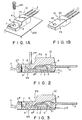
- 1 denotes a semiconductor chip
- Device 10 can be directly fixed on head sink 200 of, for example, aluminum by means of screw 100.
- Part of island 2 of the lead frame is kept contact with supporting pins FP until the mould formation is completed, and thus the lead frame can be adequately positioned.
- Moulded resin 6 is formed to have electrically insulative and heat-conductive thin resin film 6* formed on rear surface side BS of chip mounting section 2 and is so formed that tip end portion 2* of the lead frame will not extend out of moulded resin 6.
- the lead frame (2, 3) is formed to have a bent portion (X) so that the position (T1) of rear surface BS of chip mounting section 2 can be set lower than the position (T2) of the tip end portion 2*.
- distance T1 from the rear surface of chip mounting section 2 to the surface of resin film 6* is set to by smaller than distance T2 from the rear surface of tip end portion 2* to the surface of resin film 6*.
- front surface FS of the lead frame is exposed in frame supporting holes when rear surface side BS of semiconductor device 10 is mounted on a mounting metal plate such as heat radiation plate 200.
- a mounting metal plate such as heat radiation plate 200.
- base end plate (outer connection lead) 3 of the lead frame is first fixed with tip end portion 2* of the lead frame and chip mounting section 2 set in the metal mould. Then, molten resin 11 is injected by pressure into a space under tip end portion 2* of the lead frame via a resin inlet (provided below tip end portion 2* of the lead frame) of the metal mould. At this time, tip end portion 2* of the lead frame is lifted by the action of viscosity of molten resin 11, and the lead frame is fixed with the upper surface thereof set in contact with frame supporting pins (not shown) which are formed inside the metal mould. In this case, since no pin is provided to support rear surface BS of the lead frame, no frame supporting hole is formed in rear surface BS after the resin moulding is completed.
- Semiconductor device 10 shown in Fig. 3 is similar to the semiconductor device of the former embodiment shown in Fig. 2 except that bending angle ⁇ of the lead frame is set to a different value.
- bending angle ⁇ on the base end plate side is so set that tip end portion 2* can be positioned higher than base end plate (outer connection lead) 3 of chip mounting section 2.
- the lead frame described above has an advantage that the thickness of resin film 6* on the rear surface side can be adjusted according to the position of the supporting pins on front surface FS of the lead frame in the mould resin sealing operation.
- Semiconductor device 10 shown in Fig. 4 is similar to the semiconductor device of the former embodiment shown in Fig. 2 except for the shape of the lead frame. With the lead frame, the upper surface of chip mounting section 2 and the upper surface of tip end portion 2* are placed on the same plane, and thickness t2* of tip end portion 2* is made smaller than thickness t2 of chip mounting section 2.
- cap 5 can be omitted as the case may be.
- the tip end portion of the lead frame is formed so as not to extend out of the outer casing and no frame supporting hole is formed in the rear surface of the outer casing. Therefore, when the rear surface is mounted on a metal plate such as heat radiation plate, the dielectric strength of a portion between the lead frame and the metal plate will not be lowered. In a condition that the lead frame is mounted on the metal plate, the dielectric strength is 2 to 2.5 kV in a conventional frame fixing type semiconductor device and 3 to 3.5 kV in a conventional frame supporting type semiconductor device. In contrast, in the semiconductor device as made by the method of this invention being equivalent in scale to the above conventional semiconductor device, the dielectric strength of 5 kV or more can be obtained, and thus the dielectric strength of mould resin film 6* on the rear surface side can be significantly improved.
Landscapes
- Structures Or Materials For Encapsulating Or Coating Semiconductor Devices Or Solid State Devices (AREA)
- Encapsulation Of And Coatings For Semiconductor Or Solid State Devices (AREA)
Claims (3)
- Verfahren zur Herstellung einer Halbleitervorrichtung des Typs mit Harzisolierung, welche folgendes umfaßt: ein Außengehäuse (6) aus einem vergossenen Harz mit einer vorderen und einer hinteren Fläche;
einen Systemträger mit einem Montageabschnitt (2) für ein Halbleiterchip neben einem Spitzenendabschnitt (2*) auf der einen Seite und einem äußeren Anschlußleiter (3) auf der anderen Seite;
einen auf dem Chipmontageabschnitt (2) montierten Halbleiterchip (1),
wobei das vergossene Harzgehäuse (6) den Spitzenendabschnitt (2*) und im wesentlichen den gesamten Montageabschnitt (2) einschließt, während es den äußeren Anschlußleiter (3) freiliegend läßt und einen dünnen Harzfilm (6*) auf der hinteren Oberfläche des Systemträgers (2, 3) zur elektrischen Isolierung und Wärmeableitung bildet, und der Systemträger (2, 3) eine solche Form hat, daß ein Abstand (T2) des Spitzenendabschnitts (2*) von der hinteren Oberfläche größer ist als derjenige (T1) des Chipmontageabschnitts (2), und wobei dieses Verfahren folgende Schritte umfaßt: Bereitstellen einer Metallform mit Trägerhalterungsstiften zur Aufnahme eines Teils des Chipmontageabschnitts (2) zum Zeitpunkt der Bildung des vergossenen Harzgehäuses (6), wobei sich diese Trägerhalterungsstifte an der vorderen Fläche des Systemträgers (2, 3), jedoch nicht an seiner hinteren Fläche befinden;
Fixieren des äußeren Anschlußleiters (3) in der Metallform, so daß der Spitzenendabschnitt (2*) und der Chipmontageabschnitt (2) in der Metallform sitzen;
Einspritzen von viskosem, geschmolzenem Harz unter Druck in die Metallform und den Raum unter dem Spitzenendabschnitt (2*), so daß der Spitzenendabschnitt (2*) durch das geschmolzene Harz angehoben wird, und der Systemträger (2, 3) an der vorderen Fläche des Chipmontageabschnitts (2), welche mit den Trägerhalterungsstiften der Metallform in Berührung steht, fixiert wird;
Aufrechterhalten des Kontaktes zwischen dem Chipmontageabschnitt (2) und den Trägerhalterungsstiften, bis die Bildung des vergossenen Harzgehäuses (6) abgeschlossen ist. - Verfahren zur Herstellung einer Halbleitervorrichtung des Typs mit Harzisolierung gemäß Anspruch 1, dadurch gekennzeichnet, daß der Montageabschnitt (2) für den Halbleiterchip so ausgeformt ist, daß er einen gebogenen Abschnitt zwischen dem äußeren Anschlußleiter (3) und dem Montageabschnitt (2) für den Halbleiterchip aufweist, dessen Biegewinkel so bestimmt wird, daß der Abstand des Spitzenendabschnitts (2*) des Systemträgers (2, 3) vom Harzfilm auf der hinteren Oberfläche (6*) größer ist als derjenige des äußeren Anschlußleiters (3) vom Harzfilm auf der hinteren Oberfläche (6*) (T2>T1).
- Verfahren zur Herstellung einer Halbleitervorrichtung des Typs mit Harzisolierung gemäß Anspruch 1, dadurch gekennzeichnet, daß der Systemträger (2, 3) so geformt ist, daß die obere Fläche des Montageabschnitts (2) für den Halbleiterchip und die obere Fläche des Spitzenendabschnitts (2*) des Systemträgers (2, 3) in derselben Ebene positioniert sind, und die Dicke (t2*) des Spitzenendabschnitts (2*) kleiner eingestellt ist als diejenige (t2) des Montageabschnitts (2) für den Halbleiterchip.
Applications Claiming Priority (2)
| Application Number | Priority Date | Filing Date | Title |
|---|---|---|---|
| JP232945/87 | 1987-09-17 | ||
| JP62232945A JPH0815165B2 (ja) | 1987-09-17 | 1987-09-17 | 樹脂絶縁型半導体装置の製造方法 |
Publications (3)
| Publication Number | Publication Date |
|---|---|
| EP0307946A2 EP0307946A2 (de) | 1989-03-22 |
| EP0307946A3 EP0307946A3 (en) | 1989-07-05 |
| EP0307946B1 true EP0307946B1 (de) | 1994-11-17 |
Family
ID=16947315
Family Applications (1)
| Application Number | Title | Priority Date | Filing Date |
|---|---|---|---|
| EP88115240A Expired - Lifetime EP0307946B1 (de) | 1987-09-17 | 1988-09-16 | Verfahren zum Herstellen einer Halbleiteranordnung vom harzumhüllten Typ |
Country Status (5)
| Country | Link |
|---|---|
| US (1) | US5038200A (de) |
| EP (1) | EP0307946B1 (de) |
| JP (1) | JPH0815165B2 (de) |
| KR (1) | KR910009419B1 (de) |
| DE (1) | DE3852124T2 (de) |
Families Citing this family (13)
| Publication number | Priority date | Publication date | Assignee | Title |
|---|---|---|---|---|
| US5309027A (en) * | 1992-06-15 | 1994-05-03 | Motorola, Inc. | Encapsulated semiconductor package having protectant circular insulators |
| DE9311223U1 (de) * | 1993-07-27 | 1993-09-09 | Siemens AG, 80333 München | Mikrosensor mit Steckeranschluß |
| TW270213B (de) * | 1993-12-08 | 1996-02-11 | Matsushita Electric Industrial Co Ltd | |
| US5886400A (en) * | 1995-08-31 | 1999-03-23 | Motorola, Inc. | Semiconductor device having an insulating layer and method for making |
| JP3344684B2 (ja) * | 1996-05-20 | 2002-11-11 | 株式会社村田製作所 | 電子部品 |
| US6476481B2 (en) | 1998-05-05 | 2002-11-05 | International Rectifier Corporation | High current capacity semiconductor device package and lead frame with large area connection posts and modified outline |
| JP3833464B2 (ja) * | 2000-11-01 | 2006-10-11 | 株式会社三井ハイテック | リードフレーム |
| US7466016B2 (en) * | 2007-04-07 | 2008-12-16 | Kevin Yang | Bent lead transistor |
| EP2051298B1 (de) * | 2007-10-18 | 2012-09-19 | Sencio B.V. | Gehäuse mit integrierter Schaltung |
| US7839004B2 (en) * | 2008-07-30 | 2010-11-23 | Sanyo Electric Co., Ltd. | Semiconductor device, semiconductor module, method for manufacturing semiconductor device, and lead frame |
| JP2010103411A (ja) * | 2008-10-27 | 2010-05-06 | Shindengen Electric Mfg Co Ltd | 半導体装置及びその製造方法 |
| TWI425907B (zh) * | 2010-09-21 | 2014-02-01 | 台達電子工業股份有限公司 | 電子元件和散熱裝置之組合結構及其絕緣元件 |
| CN104247012B (zh) * | 2012-10-01 | 2017-08-25 | 富士电机株式会社 | 半导体装置及其制造方法 |
Family Cites Families (3)
| Publication number | Priority date | Publication date | Assignee | Title |
|---|---|---|---|---|
| JPS5946052A (ja) * | 1982-09-08 | 1984-03-15 | Nec Corp | 樹脂封止絶縁型半導体装置 |
| JPS59130449A (ja) * | 1983-01-17 | 1984-07-27 | Nec Corp | 絶縁型半導体素子用リードフレーム |
| JPS6163849U (de) * | 1984-09-29 | 1986-04-30 |
-
1987
- 1987-09-17 JP JP62232945A patent/JPH0815165B2/ja not_active Expired - Fee Related
-
1988
- 1988-09-16 EP EP88115240A patent/EP0307946B1/de not_active Expired - Lifetime
- 1988-09-16 DE DE3852124T patent/DE3852124T2/de not_active Expired - Fee Related
- 1988-09-16 KR KR1019880011977A patent/KR910009419B1/ko not_active Expired
-
1990
- 1990-11-28 US US07/618,591 patent/US5038200A/en not_active Expired - Lifetime
Non-Patent Citations (1)
| Title |
|---|
| PATENT ABSTRACTS OF JAPAN, vol. 10, no. 268 (E-436)[2324], 12th September 1986 ; & JP-A-61 91 937 * |
Also Published As
| Publication number | Publication date |
|---|---|
| DE3852124D1 (de) | 1994-12-22 |
| KR910009419B1 (ko) | 1991-11-15 |
| DE3852124T2 (de) | 1995-03-23 |
| JPS6474746A (en) | 1989-03-20 |
| KR890005860A (ko) | 1989-05-17 |
| US5038200A (en) | 1991-08-06 |
| EP0307946A3 (en) | 1989-07-05 |
| EP0307946A2 (de) | 1989-03-22 |
| JPH0815165B2 (ja) | 1996-02-14 |
Similar Documents
| Publication | Publication Date | Title |
|---|---|---|
| CA1174821A (en) | Method for manufacturing a plastic encapsulated semiconductor device and a lead frame therefor | |
| EP0063811B1 (de) | Verfahren zum Herstellen einer in Kunststoff verkapselten Halbleiteranordnung | |
| US5834835A (en) | Semiconductor device having an improved structure for storing a semiconductor chip | |
| US4503452A (en) | Plastic encapsulated semiconductor device and method for manufacturing the same | |
| US5038200A (en) | Resin insulated type semiconductor device | |
| US4750030A (en) | Resin-molded semiconductor device having heat radiating plate embedded in the resin | |
| US10388581B2 (en) | Semiconductor device having press-fit terminals disposed in recesses in a case frame | |
| KR19980032479A (ko) | 표면 설치 to-220 패키지 및 그의 제조 공정 | |
| KR100231934B1 (ko) | 반도체 장치 | |
| US7091580B2 (en) | Semiconductor device | |
| KR19980055817A (ko) | 버텀리드 반도체 패키지 및 그 제조 방법 | |
| JPH03108744A (ja) | 樹脂封止型半導体装置 | |
| JPH0897333A (ja) | 半導体モールドパッケージ | |
| JPS60128646A (ja) | 絶縁型パワートランジスタの製造方法 | |
| EP0809861B1 (de) | Methode zur herstellung eines halbleiterbauteils für oberflächenmontage, geeignet für vergleichsweise hohe spannungen und ein solches halbleiterbauteil | |
| JPH10242385A (ja) | 電力用混合集積回路装置 | |
| JPH0548955B2 (de) | ||
| JP3209120B2 (ja) | 圧力センサ | |
| JPH0254665B2 (de) | ||
| JP2555497B2 (ja) | 中空型樹脂封止半導体圧力センサ | |
| JP3014873B2 (ja) | 半導体装置の製造方法 | |
| JPS63211638A (ja) | 樹脂封止型半導体装置の製造方法 | |
| JP2802966B2 (ja) | 樹脂封止型電子部品の製造方法 | |
| CN119542150A (zh) | 半导体结构的制备方法 | |
| JPH04192351A (ja) | 半導体装置及びその形成方法 |
Legal Events
| Date | Code | Title | Description |
|---|---|---|---|
| PUAI | Public reference made under article 153(3) epc to a published international application that has entered the european phase |
Free format text: ORIGINAL CODE: 0009012 |
|
| 17P | Request for examination filed |
Effective date: 19881013 |
|
| AK | Designated contracting states |
Kind code of ref document: A2 Designated state(s): DE FR GB |
|
| PUAL | Search report despatched |
Free format text: ORIGINAL CODE: 0009013 |
|
| AK | Designated contracting states |
Kind code of ref document: A3 Designated state(s): DE FR GB |
|
| 17Q | First examination report despatched |
Effective date: 19920303 |
|
| GRAA | (expected) grant |
Free format text: ORIGINAL CODE: 0009210 |
|
| AK | Designated contracting states |
Kind code of ref document: B1 Designated state(s): DE FR GB |
|
| REF | Corresponds to: |
Ref document number: 3852124 Country of ref document: DE Date of ref document: 19941222 |
|
| ET | Fr: translation filed | ||
| PLBE | No opposition filed within time limit |
Free format text: ORIGINAL CODE: 0009261 |
|
| STAA | Information on the status of an ep patent application or granted ep patent |
Free format text: STATUS: NO OPPOSITION FILED WITHIN TIME LIMIT |
|
| 26N | No opposition filed | ||
| PGFP | Annual fee paid to national office [announced via postgrant information from national office to epo] |
Ref country code: FR Payment date: 19970909 Year of fee payment: 10 |
|
| PGFP | Annual fee paid to national office [announced via postgrant information from national office to epo] |
Ref country code: DE Payment date: 19970919 Year of fee payment: 10 |
|
| REG | Reference to a national code |
Ref country code: GB Ref legal event code: 746 Effective date: 19981103 |
|
| PG25 | Lapsed in a contracting state [announced via postgrant information from national office to epo] |
Ref country code: FR Free format text: LAPSE BECAUSE OF NON-PAYMENT OF DUE FEES Effective date: 19990531 |
|
| PG25 | Lapsed in a contracting state [announced via postgrant information from national office to epo] |
Ref country code: DE Free format text: LAPSE BECAUSE OF NON-PAYMENT OF DUE FEES Effective date: 19990701 |
|
| REG | Reference to a national code |
Ref country code: FR Ref legal event code: ST |
|
| REG | Reference to a national code |
Ref country code: GB Ref legal event code: IF02 |
|
| PGFP | Annual fee paid to national office [announced via postgrant information from national office to epo] |
Ref country code: GB Payment date: 20050914 Year of fee payment: 18 |
|
| GBPC | Gb: european patent ceased through non-payment of renewal fee |
Effective date: 20060916 |
|
| PG25 | Lapsed in a contracting state [announced via postgrant information from national office to epo] |
Ref country code: GB Free format text: LAPSE BECAUSE OF NON-PAYMENT OF DUE FEES Effective date: 20060916 |