EP0307959B1 - Dispositif à cristal liquide ferroélectrique smectique - Google Patents
Dispositif à cristal liquide ferroélectrique smectique Download PDFInfo
- Publication number
- EP0307959B1 EP0307959B1 EP88115325A EP88115325A EP0307959B1 EP 0307959 B1 EP0307959 B1 EP 0307959B1 EP 88115325 A EP88115325 A EP 88115325A EP 88115325 A EP88115325 A EP 88115325A EP 0307959 B1 EP0307959 B1 EP 0307959B1
- Authority
- EP
- European Patent Office
- Prior art keywords
- alignment
- liquid crystal
- domain
- alignment state
- state
- Prior art date
- Legal status (The legal status is an assumption and is not a legal conclusion. Google has not performed a legal analysis and makes no representation as to the accuracy of the status listed.)
- Expired - Lifetime
Links
- 239000004990 Smectic liquid crystal Substances 0.000 title claims description 63
- 239000004973 liquid crystal related substance Substances 0.000 claims description 62
- 230000007547 defect Effects 0.000 claims description 56
- 230000008033 biological extinction Effects 0.000 claims description 26
- 239000000758 substrate Substances 0.000 claims description 26
- 229920001721 polyimide Polymers 0.000 claims description 11
- 238000007789 sealing Methods 0.000 claims description 4
- 239000004952 Polyamide Substances 0.000 claims description 2
- 229920002647 polyamide Polymers 0.000 claims description 2
- 229920006267 polyester film Polymers 0.000 claims 1
- 210000004027 cell Anatomy 0.000 description 51
- 239000005262 ferroelectric liquid crystals (FLCs) Substances 0.000 description 17
- 210000002858 crystal cell Anatomy 0.000 description 16
- 230000007704 transition Effects 0.000 description 13
- 230000005684 electric field Effects 0.000 description 12
- 239000002052 molecular layer Substances 0.000 description 11
- 230000000052 comparative effect Effects 0.000 description 10
- 239000011521 glass Substances 0.000 description 9
- 238000002834 transmittance Methods 0.000 description 9
- 239000004642 Polyimide Substances 0.000 description 8
- 239000000203 mixture Substances 0.000 description 8
- VYPSYNLAJGMNEJ-UHFFFAOYSA-N Silicium dioxide Chemical compound O=[Si]=O VYPSYNLAJGMNEJ-UHFFFAOYSA-N 0.000 description 6
- 239000011324 bead Substances 0.000 description 6
- 239000000463 material Substances 0.000 description 6
- 230000003287 optical effect Effects 0.000 description 6
- 230000001154 acute effect Effects 0.000 description 5
- 238000002474 experimental method Methods 0.000 description 5
- 238000007740 vapor deposition Methods 0.000 description 5
- 125000002723 alicyclic group Chemical group 0.000 description 4
- KFZMGEQAYNKOFK-UHFFFAOYSA-N Isopropanol Chemical compound CC(C)O KFZMGEQAYNKOFK-UHFFFAOYSA-N 0.000 description 3
- PNEYBMLMFCGWSK-UHFFFAOYSA-N aluminium oxide Inorganic materials [O-2].[O-2].[O-2].[Al+3].[Al+3] PNEYBMLMFCGWSK-UHFFFAOYSA-N 0.000 description 3
- 230000015572 biosynthetic process Effects 0.000 description 3
- 230000008859 change Effects 0.000 description 3
- 230000003098 cholesteric effect Effects 0.000 description 3
- 238000005259 measurement Methods 0.000 description 3
- 230000002093 peripheral effect Effects 0.000 description 3
- 230000004044 response Effects 0.000 description 3
- 230000000717 retained effect Effects 0.000 description 3
- 230000002441 reversible effect Effects 0.000 description 3
- 239000000377 silicon dioxide Substances 0.000 description 3
- 125000006850 spacer group Chemical group 0.000 description 3
- 230000035882 stress Effects 0.000 description 3
- GWEVSGVZZGPLCZ-UHFFFAOYSA-N Titan oxide Chemical compound O=[Ti]=O GWEVSGVZZGPLCZ-UHFFFAOYSA-N 0.000 description 2
- 125000003118 aryl group Chemical group 0.000 description 2
- 238000001816 cooling Methods 0.000 description 2
- 230000006355 external stress Effects 0.000 description 2
- PJXISJQVUVHSOJ-UHFFFAOYSA-N indium(III) oxide Inorganic materials [O-2].[O-2].[O-2].[In+3].[In+3] PJXISJQVUVHSOJ-UHFFFAOYSA-N 0.000 description 2
- AMGQUBHHOARCQH-UHFFFAOYSA-N indium;oxotin Chemical compound [In].[Sn]=O AMGQUBHHOARCQH-UHFFFAOYSA-N 0.000 description 2
- 239000007788 liquid Substances 0.000 description 2
- XOLBLPGZBRYERU-UHFFFAOYSA-N tin dioxide Chemical compound O=[Sn]=O XOLBLPGZBRYERU-UHFFFAOYSA-N 0.000 description 2
- POAOYUHQDCAZBD-UHFFFAOYSA-N 2-butoxyethanol Chemical compound CCCCOCCO POAOYUHQDCAZBD-UHFFFAOYSA-N 0.000 description 1
- QTBSBXVTEAMEQO-UHFFFAOYSA-M Acetate Chemical compound CC([O-])=O QTBSBXVTEAMEQO-UHFFFAOYSA-M 0.000 description 1
- SECXISVLQFMRJM-UHFFFAOYSA-N N-Methylpyrrolidone Chemical compound CN1CCCC1=O SECXISVLQFMRJM-UHFFFAOYSA-N 0.000 description 1
- 230000001133 acceleration Effects 0.000 description 1
- 230000005540 biological transmission Effects 0.000 description 1
- 239000003795 chemical substances by application Substances 0.000 description 1
- 239000011248 coating agent Substances 0.000 description 1
- 238000000576 coating method Methods 0.000 description 1
- 229910052681 coesite Inorganic materials 0.000 description 1
- 229910052906 cristobalite Inorganic materials 0.000 description 1
- 239000013078 crystal Substances 0.000 description 1
- 230000006866 deterioration Effects 0.000 description 1
- 238000001035 drying Methods 0.000 description 1
- 239000004744 fabric Substances 0.000 description 1
- 230000006870 function Effects 0.000 description 1
- 238000010438 heat treatment Methods 0.000 description 1
- 238000004519 manufacturing process Methods 0.000 description 1
- 238000000034 method Methods 0.000 description 1
- 229920000728 polyester Polymers 0.000 description 1
- 230000003252 repetitive effect Effects 0.000 description 1
- 230000004043 responsiveness Effects 0.000 description 1
- 230000000630 rising effect Effects 0.000 description 1
- 229910052682 stishovite Inorganic materials 0.000 description 1
- PBCFLUZVCVVTBY-UHFFFAOYSA-N tantalum pentoxide Inorganic materials O=[Ta](=O)O[Ta](=O)=O PBCFLUZVCVVTBY-UHFFFAOYSA-N 0.000 description 1
- 229910052905 tridymite Inorganic materials 0.000 description 1
Images




Classifications
-
- G—PHYSICS
- G02—OPTICS
- G02F—OPTICAL DEVICES OR ARRANGEMENTS FOR THE CONTROL OF LIGHT BY MODIFICATION OF THE OPTICAL PROPERTIES OF THE MEDIA OF THE ELEMENTS INVOLVED THEREIN; NON-LINEAR OPTICS; FREQUENCY-CHANGING OF LIGHT; OPTICAL LOGIC ELEMENTS; OPTICAL ANALOGUE/DIGITAL CONVERTERS
- G02F1/00—Devices or arrangements for the control of the intensity, colour, phase, polarisation or direction of light arriving from an independent light source, e.g. switching, gating or modulating; Non-linear optics
- G02F1/01—Devices or arrangements for the control of the intensity, colour, phase, polarisation or direction of light arriving from an independent light source, e.g. switching, gating or modulating; Non-linear optics for the control of the intensity, phase, polarisation or colour
- G02F1/13—Devices or arrangements for the control of the intensity, colour, phase, polarisation or direction of light arriving from an independent light source, e.g. switching, gating or modulating; Non-linear optics for the control of the intensity, phase, polarisation or colour based on liquid crystals, e.g. single liquid crystal display cells
- G02F1/137—Devices or arrangements for the control of the intensity, colour, phase, polarisation or direction of light arriving from an independent light source, e.g. switching, gating or modulating; Non-linear optics for the control of the intensity, phase, polarisation or colour based on liquid crystals, e.g. single liquid crystal display cells characterised by the electro-optical or magneto-optical effect, e.g. field-induced phase transition, orientation effect, guest-host interaction or dynamic scattering
- G02F1/139—Devices or arrangements for the control of the intensity, colour, phase, polarisation or direction of light arriving from an independent light source, e.g. switching, gating or modulating; Non-linear optics for the control of the intensity, phase, polarisation or colour based on liquid crystals, e.g. single liquid crystal display cells characterised by the electro-optical or magneto-optical effect, e.g. field-induced phase transition, orientation effect, guest-host interaction or dynamic scattering based on orientation effects in which the liquid crystal remains transparent
- G02F1/141—Devices or arrangements for the control of the intensity, colour, phase, polarisation or direction of light arriving from an independent light source, e.g. switching, gating or modulating; Non-linear optics for the control of the intensity, phase, polarisation or colour based on liquid crystals, e.g. single liquid crystal display cells characterised by the electro-optical or magneto-optical effect, e.g. field-induced phase transition, orientation effect, guest-host interaction or dynamic scattering based on orientation effects in which the liquid crystal remains transparent using ferroelectric liquid crystals
- G02F1/1416—Details of the smectic layer structure, e.g. bookshelf, chevron, C1 and C2
Definitions
- the domain occupying a major proportion of the device area comprises the liquid crystal in a first alignment state wherein the liquid crystal forms a connected pair of a hair pin defect and a lightning defect so that the hair pin defect is formed after the lightning defect in the uniaxial alignment axis direction.
- the liquid crystal used was a ferroelectric smectic liquid crystal "CS-1014" (trade name, available from Chisso K.K.).
- the alignment film was formed by using an alicyclic polyimide film-forming liquid "SUN-EVER 150" (trade name, available from Nissan Kagaku Kogyo K.K.).
- the pair of substrates were provided with rubbing axes which were in parallel with each other and identical in direction. (The details of the production of the cell are the same as those given in Example 1 appearing hereinafter except for the cell size and the absence of spacer beads.)
- the liquid crystal in the cell showed the following phase transition characteristic (the numbers indicated on the arrows denote phase transition temperatures in °C):
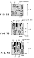
- Figure 2 shows the extinction state (the state given by the extinction position of right angle cross nicols providing the darkest condition of the dark state) of a C1 alignment domain 20 at 52.0 °C, which is bluish including a blue bright state 21 and a blue dark state 22.
- Figure 6 shows a blackish extinction state of a C2 alignment domain 30 at 25 °C including a white bright state 31 and a black dark state 32.
- Figures 3 to 5 respectively show a mixture domain 40 including a bluish extinction state of a C1 alignment domain 20 and a blackish extinction state of a C2 alignment domain 30 at 51.3 °C, 51.2 °C and 51.1 °C, respectively.
- the cell provided a C1 alignment domain or sub-phase 20 and a C2 alignment domain or sub-phase 30, which are different from each other, in the temperature range of chiral smectic C phase.
- the C2 alignment domain 30 was gradually grown to occupy a major areal proportion (60 % or more, preferably 90 % or more) and the C1 alignment domain 20 shrinked correspondingly to occupy a minor areal proportion (40 % or less, preferably 10 % or less) until it reached a macroscopically or substantially negligible except for a minor portion in the vicinity of the cell periphery as is shown in Figures 3 to 5.
- Figures 7A and 7B are a partial schematic plan view and a corresponding sectional view, respectively, showing a hair pin defect and a lightning defect formed in a generally C1 alignment domain.
- Figures 7C and 7D are a partial schematic plan view and a corresponding sectional view, respectively, showing a hair pin defect and a lightning defect formed in a generally C2 alignment domain.
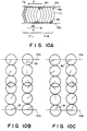
- Figure 9B shows a typical pair of twisting arrangements of C director 81 oriented in a C2 alignment state.
- Molecular long axes 80 in a molecular layer 71 are arranged while changing their positions on the bases 83 (circles) of cones 82 between the interface with the upper alignment control film 14a and the interface with the lower alignment control film 14b.
- the right half arrangement and the left half arrangement of each of Figures 8B and 9B correspond to orientation states after application of a positive (or negative) polarity pulse and a negative (or positive) polarity pulse.
- a molecular layer 71 forms an acute inclination angle ⁇ A on both the upper and lower alignment control films in the C1 alignment domain 73, and an obtuse angle ⁇ B on both the upper and lower alignment control films in the C2 alignment domain 74.
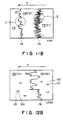
- Figure 12 (12A and 12B) shows connected pairs of a small hair pin defect 121 and a small lightning defect 122 generated due to the presence of spacer beads (of alumina or silica in an average diameter of about 1.5 microns) respectively in a C1 alignment domain 73 and a C2 alignment domain 74 formed with a hair pin defect 76 at the boundary therebetween.
- spacer beads of alumina or silica in an average diameter of about 1.5 microns
- a temperature range for providing a C1 alignment state wherein a lightning defect is formed after a hair pin defect may be restricted to 1/5 or below, preferably 1/10 or below, further preferably 1/20 or below, of a temperature range for providing a C2 alignment state wherein a hair pin defect is formed after a lightning defect, respectively in the direction of a uniaxial alignment axis.
- the lower temperature limit in the course of temperature decrease for allowing the presence of the C1 alignment state or domain in a substantial proportion (40 % or above, preferably 10 % or above) should be 30 °C or higher, preferably 40 °C or higher.
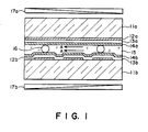
- a surface-stabilized-type ferroelectric liquid crystal cell in a bistable alignment state used in the liquid crystal device of the present invention may be made sufficiently thin.
- the liquid crystal layer is sufficiently thin (e.g., 0.1 - 3 microns)
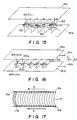
- the helical structure of the liquid crystal molecules will be unwound even under no application of electrical field to become a nonhelical structure as shown in Figure 16, whereby its dipole moment assumes either Pa directed upward (164a) or Pb directed downward (164b), thus forming a bistable state.
- the above-prepared liquid crystal cell was sandwiched between a pair of right-angle cross nicol polarizers and then supplied with a pulse of 50 ⁇ sec and 30 V. Then, the right-angle cross nicols were set at the extinction position (to provide the darkest state), and the transmittance of the cell at that time was measured by a photomultiplier. Then, a pulse of 50 ⁇ sec and -30 V was applied to the cell to provide a bright state, and the transmittance at that time was measured in the same manner. As a result, the transmittance in the darkest state was 1.0 % and the transmittance in the bright state was 8.0 %, so that a contrast of 8 was obtained.
- Ferroelectric smectic liquid crystal cells were prepared in the same manner as in Example 1 except that alignment control film materials and liquid crystal materials shown in the following Table 4 were used.
Landscapes
- Physics & Mathematics (AREA)
- Chemical & Material Sciences (AREA)
- Crystallography & Structural Chemistry (AREA)
- Nonlinear Science (AREA)
- General Physics & Mathematics (AREA)
- Optics & Photonics (AREA)
- Liquid Crystal (AREA)
Claims (21)
- Dispositif à cristaux liquides smectiques chiraux, comprenant :a) une paire de substrats présentant chacun un axe d'alignement uniaxial dans des directions qui sont identiques et essentiellement parallèles l'une à l'autre ;b) un cristal liquide smectique chiral disposé suivant une phase C smectique chirale à structure non hélicoïdale présentant deux états d'orientation stables entre les substrats, le cristal liquide formant un domaine à un premier état d'alignement C2 développé de manière à occuper une portion dominante de surface, égale ou supérieure à 60 % de la surface totale du dispositif lors d'un abaissement de la température, dans lequel ledit domaine occupant une portion dominante de la surface du dispositif comprend une pluralité de couches constituées chacune d'une pluralité de molécules de cristal liquide et fléchies à partir des deux substrats dans une direction qui est identique à la direction d'axe d'alignement uniaxial, par oppositoin aux couches dans un domaine à l'état d'orientation C1 qui sont fléchies dans une direction qui est opposée à la direction d'axe d'alignement uniaxial, etc) un moyen pour différencier optiquement les deux états d'orientation stables.
- Dispositif suivant la revendication 1, dans lequel le domaine occupant une proportion dominante de la surface du dispositif comprend le cristal liquide dans un premier état d'alignement dans lequel le cristal liquide forme une paire connectée d'un défaut en épingle à cheveux et d'un défaut d'impulsion lumineuse de telle sorte que le défaut en épingle à cheveux soit formé après le défaut d'impulsion lumineuse dans la direction d'axe d'alignement uniaxial.
- Dispositif suivant la revendication 2, dans lequel la plage de températures où le domaine dans l'autre état d'alignement n'occupe pas une proportion secondaire représente une valeur égale ou inférieure à 1/5 de la plage de températures où le domaine dans l'autre état d'alignement occupe une proportion secondaire, respectivement, au cours de l'abaissement de la température.
- Dispositif suivant la revendication 2, dans lequel la plage de températures où le domaine dans l'autre état d'alignement n'occupe pas une proportion secondaire représente une valeur égale ou inférieure à 1/10 de la plage de températures où le domaine dans l'autre état d'alignement occupe une proportion secondaire, respectivement, au cours de l'abaissement de la température.
- Dispositif suivant la revendication 2, dans lequel la plage de températures où le domaine dans l'autre état d'alignement n'occupe pas une proportion secondaire représente une valeur égale ou inférieure à 1/20 de la plage de températures où le domaine dans l'autre état d'alignement occupe une proportion secondaire, respectivement, au cours de l'abaissement de la température.
- Dispositif suivant la revendication 2, dans lequel la limite inférieure de la plage de températures où le domaine dans l'autre état d'alignement n'occupe pas une proportion secondaire est égale ou supérieure à 30°C au cours de l'abaissement de la température.
- Dispositif suivant la revendication 2, dans lequel la limite inférieure de la plage de températures où le domaine dans l'autre état d'alignement n'occupe pas une proportion secondaire est égale ou supérieure à 40°C au cours de l'abaissement de la température.
- Dispositif suivant la revendication 2, dans lequel le domaine dans l'autre état d'alignement est présent dans la région voisine d'un élément d'étanchéité dans une cellule, et le domaine dans le premier état d'alignement est présent à l'intérieur de la région voisine.
- Dispositif suivant la revendication 2, dans lequel l'autre état d'alignement comporte une paire connectée d'un défaut en épingle à cheveux et d'un défaut d'impulsion lumineuse, le défaut d'impulsion lumineuse étant formé après le défaut en épingle à cheveux.
- Dispositif suivant la revendication 2, dans lequel les deux états d'orientation stables dans le domaine dans le premier état d'alignement sont optiquement équivalents, respectivement, par la position d'extinction.
- Dispositif suivant la revendication 2, dans lequel l'axe d'alignement uniaxial a été communiqué à un film de commande d'alignement formé sur un substrat.
- Dispositif suivant la revendication 11, dans lequel le film de commande d'alignement comprend un film de polyimide, un film de polyamide ou un film de polyester.
- Dispositif suivant la revendication 11, dans lequel le film de commande d'alignement comprend un film de polyimide.
- Dispositif suivant la revendication 11, dans lequel le film de commande d'alignement est formé sur le substrat au moyen d'un film isolant.
- Dispositif suivant la revendication 2, dans lequel l'axe d'alignement uniaxial est un axe de frottement.
- Dispositif à cristaux liquides smectiques chiraux suivant la revendication 1, dans lequel les molécules de cristal liquide sont alignées pour former un angle de pré-inclinaison égal ou supérieur à 2 degrés par rapport à une face de substrat dans la plage de températures de la phase A smectique, ledit cristal liquide smectique chiral ayant été formé en passant par la phase smectique A lors de l'abaissement de la température.
- Dispositif suivant la revendication 16, dans lequel l'angle de pré-inclinaison est égal ou supérieur à 3 degrés.
- Dispositif suivant la revendication 16, dans lequel l'axe d'alignement uniaxial a été communiqué à un film de commande d'alignement formé sur un substrat.
- Dispositif suivant la revendication 18, dans lequel le film de commande d'alignement comprend un film de polyimide.
- Dispositif suivant la revendication 18, dans lequel le film de commande d'alignement est formé sur le substrat au moyen d'un film isolant.
- Dispositif suivant la revendication 16, dans lequel l'axe d'alignement uniaxial est un axe de frottement.
Priority Applications (1)
| Application Number | Priority Date | Filing Date | Title |
|---|---|---|---|
| EP96103081A EP0724184A1 (fr) | 1987-09-17 | 1988-09-19 | Dispositif à liquide crystal ferroélectrique |
Applications Claiming Priority (6)
| Application Number | Priority Date | Filing Date | Title |
|---|---|---|---|
| JP234357/87 | 1987-09-17 | ||
| JP23435787 | 1987-09-17 | ||
| JP232502/87 | 1987-09-18 | ||
| JP62232502A JP2681779B2 (ja) | 1987-09-18 | 1987-09-18 | 液晶セル |
| JP22504988A JP2603308B2 (ja) | 1987-09-17 | 1988-09-07 | カイラルスメクチック液晶素子及び製法 |
| JP225049/88 | 1988-09-07 |
Related Child Applications (2)
| Application Number | Title | Priority Date | Filing Date |
|---|---|---|---|
| EP96103081A Division EP0724184A1 (fr) | 1987-09-17 | 1988-09-19 | Dispositif à liquide crystal ferroélectrique |
| EP96103081.4 Division-Into | 1996-02-29 |
Publications (3)
| Publication Number | Publication Date |
|---|---|
| EP0307959A2 EP0307959A2 (fr) | 1989-03-22 |
| EP0307959A3 EP0307959A3 (fr) | 1991-03-13 |
| EP0307959B1 true EP0307959B1 (fr) | 1997-07-16 |
Family
ID=27330989
Family Applications (2)
| Application Number | Title | Priority Date | Filing Date |
|---|---|---|---|
| EP96103081A Withdrawn EP0724184A1 (fr) | 1987-09-17 | 1988-09-19 | Dispositif à liquide crystal ferroélectrique |
| EP88115325A Expired - Lifetime EP0307959B1 (fr) | 1987-09-17 | 1988-09-19 | Dispositif à cristal liquide ferroélectrique smectique |
Family Applications Before (1)
| Application Number | Title | Priority Date | Filing Date |
|---|---|---|---|
| EP96103081A Withdrawn EP0724184A1 (fr) | 1987-09-17 | 1988-09-19 | Dispositif à liquide crystal ferroélectrique |
Country Status (4)
| Country | Link |
|---|---|
| US (1) | US4932758A (fr) |
| EP (2) | EP0724184A1 (fr) |
| AU (1) | AU606456B2 (fr) |
| DE (1) | DE3855962T2 (fr) |
Families Citing this family (48)
| Publication number | Priority date | Publication date | Assignee | Title |
|---|---|---|---|---|
| FR2618587B1 (fr) * | 1987-07-20 | 1992-04-24 | Commissariat Energie Atomique | Ecran a cristal liquide, a electrodes opacifiees dans la zone non commutable de l'ecran et procedes d'obtention d'espaceurs et de traitement de cet ecran |
| US5200848A (en) * | 1987-09-17 | 1993-04-06 | Canon Kabushiki Kaisha | Ferroelectric smectic liquid crystal device |
| US5422749A (en) * | 1987-09-17 | 1995-06-06 | Canon Kabushiki Kaisha | Ferroelectric smetic liquid crystal device |
| US5268780A (en) * | 1989-05-11 | 1993-12-07 | Canon Kabushiki Kaisha | Liquid crystal device having a polyimide alignment film substituted with fluorine or a fluorine-containing group |
| JPH01179915A (ja) * | 1988-01-11 | 1989-07-18 | Canon Inc | 液晶素子 |
| US5082352A (en) * | 1988-09-29 | 1992-01-21 | Canon Kabushiki Kaisha | Ferroelectric liquid crystal apparatus |
| JP2640259B2 (ja) * | 1988-12-20 | 1997-08-13 | キヤノン株式会社 | 強誘電性液晶素子 |
| US5076671A (en) * | 1988-12-22 | 1991-12-31 | Canon Kabushiki Kaisha | Liquid crystal device having two bistable orientation states in the chiral smectic temperature range |
| US5293544A (en) * | 1989-03-07 | 1994-03-08 | Canon Kabushiki Kaisha | Liquid crystal apparatus including panel having plural bent layers of liquid crystal molecules |
| AU628953B2 (en) * | 1989-04-03 | 1992-09-24 | Canon Kabushiki Kaisha | Liquid crystal apparatus |
| US5061044A (en) * | 1989-05-23 | 1991-10-29 | Citizen Watch Co., Ltd. | Ferroelectric liquid crystal display having opposingly inclined alignment films wherein the liquid crystal has one twisted and two aligned states which coexist and a driving method to produce gray scale |
| NL8901481A (nl) * | 1989-06-12 | 1991-01-02 | Philips Nv | Passieve ferro-elektrisch vloeibaar kristal weergeefinrichting en werkwijze ter vervaardiging daarvan. |
| JP2768365B2 (ja) * | 1989-06-24 | 1998-06-25 | 富士通株式会社 | 液晶組成物 |
| EP0430299A3 (en) * | 1989-12-01 | 1992-07-15 | Canon Kabushiki Kaisha | Liquid crystal device |
| GB9002105D0 (en) * | 1990-01-31 | 1990-03-28 | Stc Plc | Ferro electric liquid crystal cells |
| US5189536A (en) * | 1990-03-02 | 1993-02-23 | Canon Kabushiki Kaisha | Ferroelectric liquid crystal element having uniform high temperature alignment |
| JP2784700B2 (ja) * | 1990-08-13 | 1998-08-06 | キヤノン株式会社 | 強誘電性液晶素子 |
| JP2802685B2 (ja) * | 1991-01-08 | 1998-09-24 | キヤノン株式会社 | 強誘電性液晶装置 |
| US5347381B1 (en) * | 1991-01-25 | 1997-07-01 | Sharp Kk | Ferroelectric liquid crystal display device with molecules between hairpin and lightning defects following the lightning defects |
| JP2775527B2 (ja) * | 1991-02-01 | 1998-07-16 | キヤノン株式会社 | カイラルスメクチック液晶素子 |
| JPH04258924A (ja) * | 1991-02-13 | 1992-09-14 | Canon Inc | カイラルスメクチック液晶素子およびその製造方法 |
| JPH05150244A (ja) * | 1991-02-20 | 1993-06-18 | Canon Inc | 強誘電液晶素子 |
| US5420603A (en) * | 1991-02-20 | 1995-05-30 | Canon Kabushiki Kaisha | Display apparatus |
| JP2835787B2 (ja) * | 1991-03-22 | 1998-12-14 | キヤノン株式会社 | 強誘電性液晶素子 |
| JP2737032B2 (ja) * | 1991-03-28 | 1998-04-08 | キヤノン株式会社 | 液晶セル |
| JP2794226B2 (ja) * | 1991-04-15 | 1998-09-03 | キヤノン株式会社 | 強誘電性液晶素子の駆動装置および駆動方法 |
| EP0509490A3 (en) * | 1991-04-16 | 1993-05-26 | Canon Kabushiki Kaisha | Liquid crystal apparatus |
| JP2847331B2 (ja) * | 1991-04-23 | 1999-01-20 | キヤノン株式会社 | 液晶表示装置 |
| JP3076085B2 (ja) * | 1991-04-27 | 2000-08-14 | 株式会社半導体エネルギー研究所 | 液晶電気光学装置 |
| JPH0534697A (ja) * | 1991-07-25 | 1993-02-12 | Canon Inc | 強誘電性液晶表示素子 |
| JP2713513B2 (ja) * | 1991-08-29 | 1998-02-16 | シャープ株式会社 | 液晶表示装置 |
| ES2098416T3 (es) * | 1991-10-30 | 1997-05-01 | Canon Kk | Dispositivo de cristal liquido y aparato de visualizacion. |
| JPH05134626A (ja) * | 1991-11-11 | 1993-05-28 | Sharp Corp | 液晶素子とその駆動方法 |
| US5285304A (en) * | 1992-01-24 | 1994-02-08 | Canon Kabushiki Kaisha | Ferroelectric liquid crystal device having spacers including the thermosetting adhesive particles and the thermoplastic polymer particles |
| EP0553727B1 (fr) * | 1992-01-24 | 1998-08-05 | Canon Kabushiki Kaisha | Méthode de traitement d'un dispositif d'affichage à cristal liquide chiral smectique |
| JPH05203961A (ja) * | 1992-01-28 | 1993-08-13 | Canon Inc | 強誘電性液晶素子 |
| US5404237A (en) * | 1992-04-28 | 1995-04-04 | Katsuse; Hirofumi | Ferroelectric liquid crystal display having c2u alignment and the rewriting voltage<non-rewriting voltage |
| EP0588012B1 (fr) * | 1992-07-15 | 1997-12-03 | Canon Kabushiki Kaisha | Dispositif à cristal liquide |
| DE69318276T2 (de) * | 1992-12-25 | 1998-10-08 | Canon Kk | Flüssigkristall-Vorrichtung und Flüssigkristall-Anzeigevorrichtung |
| GB9301051D0 (en) * | 1993-01-20 | 1993-03-10 | Marconi Gec Ltd | Liquid crystal devices |
| US5781266A (en) * | 1993-09-27 | 1998-07-14 | Matsushita Electric Industrial Co., Ltd. | Ferroelectric liquid crystal display device and method for producing the same |
| GB2293889A (en) * | 1994-10-03 | 1996-04-10 | Sharp Kk | Liquid crystal device and method of making a liquid crystal device |
| US5724116A (en) * | 1995-06-06 | 1998-03-03 | Citizen Watch Co., Ltd. | Liquid crystal panel with memory function |
| US5932136A (en) * | 1995-10-20 | 1999-08-03 | Canon Kabushiki Kaisha | Liquid crystal device and liquid crystal apparatus |
| JPH11100577A (ja) * | 1997-07-31 | 1999-04-13 | Canon Inc | 液晶の配向方法、液晶素子の製造方法、該製造方法により得られる液晶素子、液晶装置 |
| US6195147B1 (en) | 1997-08-01 | 2001-02-27 | Canon Kabushiki Kaisha | Liquid crystal substrate with optical modulation region having different alignment control forces |
| US6577289B1 (en) * | 1999-03-26 | 2003-06-10 | Canon Kabushiki Kaisha | Liquid crystal device and display apparatus including the device |
| CN116113794A (zh) | 2020-09-21 | 2023-05-12 | 香港科技大学 | 高对比度铁电液晶单元 |
Family Cites Families (13)
| Publication number | Priority date | Publication date | Assignee | Title |
|---|---|---|---|---|
| JPS60156043A (ja) * | 1984-01-23 | 1985-08-16 | Canon Inc | カイラルスメクティック液晶素子 |
| JPS6167832A (ja) * | 1984-09-12 | 1986-04-08 | Canon Inc | 液晶素子 |
| GB2166256B (en) * | 1984-10-25 | 1988-06-08 | Stc Plc | Ferroelectric liquid crystal display cells |
| JPS6259922A (ja) * | 1985-09-10 | 1987-03-16 | Canon Inc | 強誘電性液晶素子 |
| EP0219336B1 (fr) * | 1985-10-14 | 1993-07-21 | Hitachi Chemical Co., Ltd. | Couche pour commander l'orientation d'un cristal liquide et application de celle-ci dans un dispositif à cristal liquide |
| JPH0685032B2 (ja) * | 1985-10-17 | 1994-10-26 | キヤノン株式会社 | カイラルスメクティック液晶素子 |
| US4820026A (en) * | 1986-03-20 | 1989-04-11 | Canon Kabushiki Kaisha | Ferroelectric liquid crystal device with modified polyvinyl alcohol alignment film |
| US4796980A (en) * | 1986-04-02 | 1989-01-10 | Canon Kabushiki Kaisha | Ferroelectric liquid crystal optical modulation device with regions within pixels to initiate nucleation and inversion |
| GB8608116D0 (en) * | 1986-04-03 | 1986-05-08 | Secr Defence | Liquid crystal devices |
| US4796979A (en) * | 1986-04-07 | 1989-01-10 | Canon Kabushiki Kaisha | Ferroelectric liquid crystal device having dual laminated alignment films |
| GB8614838D0 (en) * | 1986-06-18 | 1986-07-23 | Gen Electric Co Plc | Liquid crystal devices |
| JP2667816B2 (ja) * | 1986-09-20 | 1997-10-27 | キヤノン株式会社 | 液晶素子 |
| KR940008530B1 (ko) * | 1987-09-18 | 1994-09-22 | 가부시끼가이샤 한도 따이에네르기 겐꾸쇼 | 액정 전기 광학 장치 |
-
1988
- 1988-09-16 AU AU22338/88A patent/AU606456B2/en not_active Expired
- 1988-09-16 US US07/245,644 patent/US4932758A/en not_active Expired - Lifetime
- 1988-09-19 DE DE3855962T patent/DE3855962T2/de not_active Expired - Lifetime
- 1988-09-19 EP EP96103081A patent/EP0724184A1/fr not_active Withdrawn
- 1988-09-19 EP EP88115325A patent/EP0307959B1/fr not_active Expired - Lifetime
Also Published As
| Publication number | Publication date |
|---|---|
| DE3855962D1 (de) | 1997-08-21 |
| US4932758A (en) | 1990-06-12 |
| EP0307959A2 (fr) | 1989-03-22 |
| EP0307959A3 (fr) | 1991-03-13 |
| AU2233888A (en) | 1989-03-23 |
| EP0724184A1 (fr) | 1996-07-31 |
| DE3855962T2 (de) | 1998-02-12 |
| AU606456B2 (en) | 1991-02-07 |
Similar Documents
| Publication | Publication Date | Title |
|---|---|---|
| US4932758A (en) | Ferroelectric smectic liquid crystal device having a bistable alignment state providing two stable orientation states | |
| US5200848A (en) | Ferroelectric smectic liquid crystal device | |
| EP0703483B1 (fr) | Dispositif à cristal liquide ferroélectrique et procédé pour sa fabrication | |
| KR100220756B1 (ko) | 반강유전성 액정을 포함하는 액정판넬 및 그의 제조방법 | |
| US5189536A (en) | Ferroelectric liquid crystal element having uniform high temperature alignment | |
| US5742369A (en) | Method of aligning liquid crystals by applying an alternating electric field under periodically changing temperature | |
| EP0539992B1 (fr) | Dispositif d'affichage à cristal liquide | |
| JP2612503B2 (ja) | 液晶素子 | |
| US5422748A (en) | Liquid crystal device and display apparatus | |
| EP0637622B1 (fr) | Dispositif à cristaux liquides | |
| JP2623137B2 (ja) | カイラルスメクチック液晶素子ユニットおよびカイラルスメクチック液晶パネルの支持方法 | |
| US5594571A (en) | Ferroelectric liquid crystal device and process for production thereof | |
| US5076671A (en) | Liquid crystal device having two bistable orientation states in the chiral smectic temperature range | |
| US5422749A (en) | Ferroelectric smetic liquid crystal device | |
| CA1302550C (fr) | Dispositif a cristaux liquides smectiques ferroelectriques | |
| JPH05203961A (ja) | 強誘電性液晶素子 | |
| JP2603308B2 (ja) | カイラルスメクチック液晶素子及び製法 | |
| JPH07168188A (ja) | 液晶素子、これを用いた液晶装置、及び液晶表示装置 | |
| JP3083016B2 (ja) | 液晶の配向処理方法、及び液晶素子の製造方法 | |
| JP2614347B2 (ja) | 液晶素子及び液晶表示装置 | |
| JP2614321B2 (ja) | 液晶素子 | |
| JP2582309B2 (ja) | 液晶素子 | |
| JPH05216034A (ja) | 強誘電性液晶素子 | |
| JPH05203959A (ja) | 強誘電性液晶素子 | |
| JPH05333342A (ja) | 液晶素子 |
Legal Events
| Date | Code | Title | Description |
|---|---|---|---|
| PUAI | Public reference made under article 153(3) epc to a published international application that has entered the european phase |
Free format text: ORIGINAL CODE: 0009012 |
|
| 17P | Request for examination filed |
Effective date: 19880919 |
|
| AK | Designated contracting states |
Kind code of ref document: A2 Designated state(s): DE FR GB IT NL |
|
| PUAL | Search report despatched |
Free format text: ORIGINAL CODE: 0009013 |
|
| AK | Designated contracting states |
Kind code of ref document: A3 Designated state(s): DE FR GB IT NL |
|
| 17Q | First examination report despatched |
Effective date: 19921228 |
|
| GRAG | Despatch of communication of intention to grant |
Free format text: ORIGINAL CODE: EPIDOS AGRA |
|
| GRAH | Despatch of communication of intention to grant a patent |
Free format text: ORIGINAL CODE: EPIDOS IGRA |
|
| GRAH | Despatch of communication of intention to grant a patent |
Free format text: ORIGINAL CODE: EPIDOS IGRA |
|
| GRAA | (expected) grant |
Free format text: ORIGINAL CODE: 0009210 |
|
| AK | Designated contracting states |
Kind code of ref document: B1 Designated state(s): DE FR GB IT NL |
|
| DX | Miscellaneous (deleted) | ||
| REF | Corresponds to: |
Ref document number: 3855962 Country of ref document: DE Date of ref document: 19970821 |
|
| ET | Fr: translation filed | ||
| ITF | It: translation for a ep patent filed | ||
| PLBE | No opposition filed within time limit |
Free format text: ORIGINAL CODE: 0009261 |
|
| STAA | Information on the status of an ep patent application or granted ep patent |
Free format text: STATUS: NO OPPOSITION FILED WITHIN TIME LIMIT |
|
| 26N | No opposition filed | ||
| REG | Reference to a national code |
Ref country code: GB Ref legal event code: IF02 |
|
| PGFP | Annual fee paid to national office [announced via postgrant information from national office to epo] |
Ref country code: DE Payment date: 20070913 Year of fee payment: 20 |
|
| PGFP | Annual fee paid to national office [announced via postgrant information from national office to epo] |
Ref country code: GB Payment date: 20070919 Year of fee payment: 20 |
|
| PGFP | Annual fee paid to national office [announced via postgrant information from national office to epo] |
Ref country code: NL Payment date: 20070916 Year of fee payment: 20 Ref country code: IT Payment date: 20070926 Year of fee payment: 20 |
|
| PGFP | Annual fee paid to national office [announced via postgrant information from national office to epo] |
Ref country code: FR Payment date: 20070914 Year of fee payment: 20 |
|
| REG | Reference to a national code |
Ref country code: GB Ref legal event code: PE20 Expiry date: 20080918 |
|
| NLV7 | Nl: ceased due to reaching the maximum lifetime of a patent |
Effective date: 20080919 |
|
| PG25 | Lapsed in a contracting state [announced via postgrant information from national office to epo] |
Ref country code: NL Free format text: LAPSE BECAUSE OF EXPIRATION OF PROTECTION Effective date: 20080919 |
|
| PG25 | Lapsed in a contracting state [announced via postgrant information from national office to epo] |
Ref country code: GB Free format text: LAPSE BECAUSE OF EXPIRATION OF PROTECTION Effective date: 20080918 |