EP0308169B1 - Ladungsinjektionsschaltung - Google Patents
Ladungsinjektionsschaltung Download PDFInfo
- Publication number
- EP0308169B1 EP0308169B1 EP88308435A EP88308435A EP0308169B1 EP 0308169 B1 EP0308169 B1 EP 0308169B1 EP 88308435 A EP88308435 A EP 88308435A EP 88308435 A EP88308435 A EP 88308435A EP 0308169 B1 EP0308169 B1 EP 0308169B1
- Authority
- EP
- European Patent Office
- Prior art keywords
- photo
- circuit
- charge injection
- field effect
- substrate
- Prior art date
- Legal status (The legal status is an assumption and is not a legal conclusion. Google has not performed a legal analysis and makes no representation as to the accuracy of the status listed.)
- Expired - Lifetime
Links
Images







Classifications
-
- H—ELECTRICITY
- H10—SEMICONDUCTOR DEVICES; ELECTRIC SOLID-STATE DEVICES NOT OTHERWISE PROVIDED FOR
- H10F—INORGANIC SEMICONDUCTOR DEVICES SENSITIVE TO INFRARED RADIATION, LIGHT, ELECTROMAGNETIC RADIATION OF SHORTER WAVELENGTH OR CORPUSCULAR RADIATION
- H10F30/00—Individual radiation-sensitive semiconductor devices in which radiation controls the flow of current through the devices, e.g. photodetectors
- H10F30/20—Individual radiation-sensitive semiconductor devices in which radiation controls the flow of current through the devices, e.g. photodetectors the devices having potential barriers, e.g. phototransistors
- H10F30/21—Individual radiation-sensitive semiconductor devices in which radiation controls the flow of current through the devices, e.g. photodetectors the devices having potential barriers, e.g. phototransistors the devices being sensitive to infrared, visible or ultraviolet radiation
- H10F30/22—Individual radiation-sensitive semiconductor devices in which radiation controls the flow of current through the devices, e.g. photodetectors the devices having potential barriers, e.g. phototransistors the devices being sensitive to infrared, visible or ultraviolet radiation the devices having only one potential barrier, e.g. photodiodes
- H10F30/221—Individual radiation-sensitive semiconductor devices in which radiation controls the flow of current through the devices, e.g. photodetectors the devices having potential barriers, e.g. phototransistors the devices being sensitive to infrared, visible or ultraviolet radiation the devices having only one potential barrier, e.g. photodiodes the potential barrier being a PN homojunction
- H10F30/2218—Individual radiation-sensitive semiconductor devices in which radiation controls the flow of current through the devices, e.g. photodetectors the devices having potential barriers, e.g. phototransistors the devices being sensitive to infrared, visible or ultraviolet radiation the devices having only one potential barrier, e.g. photodiodes the potential barrier being a PN homojunction the devices comprising active layers made of only Group IV-VI materials
-
- H—ELECTRICITY
- H04—ELECTRIC COMMUNICATION TECHNIQUE
- H04N—PICTORIAL COMMUNICATION, e.g. TELEVISION
- H04N25/00—Circuitry of solid-state image sensors [SSIS]; Control thereof
- H04N25/20—Circuitry of solid-state image sensors [SSIS]; Control thereof for transforming only infrared radiation into image signals
-
- H—ELECTRICITY
- H04—ELECTRIC COMMUNICATION TECHNIQUE
- H04N—PICTORIAL COMMUNICATION, e.g. TELEVISION
- H04N25/00—Circuitry of solid-state image sensors [SSIS]; Control thereof
- H04N25/70—SSIS architectures; Circuits associated therewith
- H04N25/76—Addressed sensors, e.g. MOS or CMOS sensors
- H04N25/77—Pixel circuitry, e.g. memories, A/D converters, pixel amplifiers, shared circuits or shared components
-
- H—ELECTRICITY
- H10—SEMICONDUCTOR DEVICES; ELECTRIC SOLID-STATE DEVICES NOT OTHERWISE PROVIDED FOR
- H10F—INORGANIC SEMICONDUCTOR DEVICES SENSITIVE TO INFRARED RADIATION, LIGHT, ELECTROMAGNETIC RADIATION OF SHORTER WAVELENGTH OR CORPUSCULAR RADIATION
- H10F30/00—Individual radiation-sensitive semiconductor devices in which radiation controls the flow of current through the devices, e.g. photodetectors
- H10F30/20—Individual radiation-sensitive semiconductor devices in which radiation controls the flow of current through the devices, e.g. photodetectors the devices having potential barriers, e.g. phototransistors
- H10F30/21—Individual radiation-sensitive semiconductor devices in which radiation controls the flow of current through the devices, e.g. photodetectors the devices having potential barriers, e.g. phototransistors the devices being sensitive to infrared, visible or ultraviolet radiation
- H10F30/22—Individual radiation-sensitive semiconductor devices in which radiation controls the flow of current through the devices, e.g. photodetectors the devices having potential barriers, e.g. phototransistors the devices being sensitive to infrared, visible or ultraviolet radiation the devices having only one potential barrier, e.g. photodiodes
- H10F30/221—Individual radiation-sensitive semiconductor devices in which radiation controls the flow of current through the devices, e.g. photodetectors the devices having potential barriers, e.g. phototransistors the devices being sensitive to infrared, visible or ultraviolet radiation the devices having only one potential barrier, e.g. photodiodes the potential barrier being a PN homojunction
- H10F30/2212—Individual radiation-sensitive semiconductor devices in which radiation controls the flow of current through the devices, e.g. photodetectors the devices having potential barriers, e.g. phototransistors the devices being sensitive to infrared, visible or ultraviolet radiation the devices having only one potential barrier, e.g. photodiodes the potential barrier being a PN homojunction the devices comprising active layers made of only Group II-VI materials, e.g. HgCdTe infrared photodiodes
-
- H—ELECTRICITY
- H10—SEMICONDUCTOR DEVICES; ELECTRIC SOLID-STATE DEVICES NOT OTHERWISE PROVIDED FOR
- H10F—INORGANIC SEMICONDUCTOR DEVICES SENSITIVE TO INFRARED RADIATION, LIGHT, ELECTROMAGNETIC RADIATION OF SHORTER WAVELENGTH OR CORPUSCULAR RADIATION
- H10F30/00—Individual radiation-sensitive semiconductor devices in which radiation controls the flow of current through the devices, e.g. photodetectors
- H10F30/20—Individual radiation-sensitive semiconductor devices in which radiation controls the flow of current through the devices, e.g. photodetectors the devices having potential barriers, e.g. phototransistors
- H10F30/21—Individual radiation-sensitive semiconductor devices in which radiation controls the flow of current through the devices, e.g. photodetectors the devices having potential barriers, e.g. phototransistors the devices being sensitive to infrared, visible or ultraviolet radiation
- H10F30/22—Individual radiation-sensitive semiconductor devices in which radiation controls the flow of current through the devices, e.g. photodetectors the devices having potential barriers, e.g. phototransistors the devices being sensitive to infrared, visible or ultraviolet radiation the devices having only one potential barrier, e.g. photodiodes
- H10F30/221—Individual radiation-sensitive semiconductor devices in which radiation controls the flow of current through the devices, e.g. photodetectors the devices having potential barriers, e.g. phototransistors the devices being sensitive to infrared, visible or ultraviolet radiation the devices having only one potential barrier, e.g. photodiodes the potential barrier being a PN homojunction
- H10F30/2215—Individual radiation-sensitive semiconductor devices in which radiation controls the flow of current through the devices, e.g. photodetectors the devices having potential barriers, e.g. phototransistors the devices being sensitive to infrared, visible or ultraviolet radiation the devices having only one potential barrier, e.g. photodiodes the potential barrier being a PN homojunction the devices comprising active layers made of only Group III-V materials
-
- H—ELECTRICITY
- H10—SEMICONDUCTOR DEVICES; ELECTRIC SOLID-STATE DEVICES NOT OTHERWISE PROVIDED FOR
- H10F—INORGANIC SEMICONDUCTOR DEVICES SENSITIVE TO INFRARED RADIATION, LIGHT, ELECTROMAGNETIC RADIATION OF SHORTER WAVELENGTH OR CORPUSCULAR RADIATION
- H10F39/00—Integrated devices, or assemblies of multiple devices, comprising at least one element covered by group H10F30/00, e.g. radiation detectors comprising photodiode arrays
- H10F39/10—Integrated devices
- H10F39/12—Image sensors
- H10F39/15—Charge-coupled device [CCD] image sensors
- H10F39/157—CCD or CID infrared image sensors
- H10F39/1575—CCD or CID infrared image sensors of the hybrid type
Definitions
- the present invention generally relates to charge injection circuits, and more particularly to a charge injection circuit for an infrared detector element which carries out a signal multiplexing within the element by coupling a photo-voltaic element and a signal processing circuit.
- An infrared detector element which carries out a signal multiplexing within the element by coupling a photo-voltaic element and a signal processing circuit such as a charge coupled device (CCD) is the center of attention as the infrared detector element of the next generation, and active research is made on the infrared detector element.
- CCD charge coupled device
- the infrared detector element In the infrared detector element, a charge (photocurrent) which is obtained by the photoelectric conversion carried out in the photo-voltaic element is injected to the signal processing circuit through a field effect transistor (FET).
- FET field effect transistor
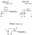
- FIG.1A shows a first example of a conventional charge injection circuit.
- This charge injection circuit is referred to as a "direct injection type" because a cathode of a photo-voltaic element 1 is directly connected to a source diffusion layer of a metal oxide semiconductor (MOS) type FET 2.
- MOS metal oxide semiconductor
- a gate of the FET 2 is applied with a gate voltage Vg through an input terminal 3.
- a drain of the FET 2 is connected to a signal processing circuit (not shown) such as a CCD to which the charge is to be injected.
- FIG.1B shows an A.C. equivalent circuit diagram of the direct injection type charge injection circuit shown in FIG.1A.
- a current source 4 of the photo-voltaic element 1 generates a photocurrent I P when the photo-voltaic element 1 receives an infrared light.
- the photocurrent I P is divided into an internal resistance R0 of the photo-voltaic element 1 and an input impedance 1/gm which is an inverse number of a mutual conductance gm of the FET 2.
- a charge corresponding to a current I2 which flows through the input impedance 1/gm is injected to the signal processing circuit.
- I1 a current which flows through the internal resistance R0
- the current I2 can be described by the following formula (1), where gm ⁇ R0/(1 + gm ⁇ R0) is the injection efficiency.
- I2 gm ⁇ R0 ⁇ I P /(1 + gm ⁇ R0)
- the internal resistance R0 is a relatively small resistance in the order of 10 k ⁇ to 1 G ⁇ . Moreover, the internal resistance R0 greatly decreases as the cutoff wavelength of the photo-voltaic element 1 becomes long and the ambient temperature becomes high.
- the input impedance 1/gm is normally dependent on the shape, that is, the width-to-length ratio of the FET 2. Under the normal operating condition, however, the operating region of the FET is in the weak inversion state, and the input impedance 1/gm is virtually independent of the width-to-length ratio of the FET 2 with respect to a current having a minute level in the weak inversion state.
- the charge corresponding to the current I2 injected to the signal processing circuit is considerably small, and the conventional charge injection circuit suffers problems in that the injection efficiency is poor and the sensitivity of the infrared detector element accordingly becomes poor.
- FIG.2 shows a second example of a conventional charge injection circuit.
- This charge injection circuit is referred to as a "gate input type" because the cathode of the photo-voltaic element 1 is directly connected to the gate of the FET 2.
- the source of the FET 2 is grounded, and the drain of the FET 2 is connected to the signal processing circuit (not shown) to which the charge is to be injected.
- the charge (photocurrent) obtained by the photoelectric conversion in the photo-voltaic element is injected to the signal processing circuit and it is important that a signal-to-noise (S/N) ratio thereof is large.
- the photo-voltaic element 1 generates the photocurrent when the infrared light is received, and the gate of the FET 2 is applied with a voltage which is determined by a product of the internal resistance R0 of the photo-voltaic element 1 and the photocurrent.
- the charge corresponding to the drain current of the FET 2 is injected to the signal processing circuit.
- the charge injected to the signal processing circuit is not directly related to the quantity of the infrared light received by the photo-voltaic element 1, and the relationship between the injected charge and the quantity of received infrared light is described by an exponential function.
- the conventional charge injection circuit uses the photo-voltaic effect, that is, an open voltage of the photo-voltaic element 1, the signal conversion is extremely faint because of the extremely small open voltage which is in the order of mV.
- the S/N ratio of the charge supplied to the signal processing circuit is poor. It is possible to conceive an arrangement wherein the open voltage is increased by providing an amplifier between the cathode of the photo-voltaic element 1 and the gate of the FET 2, but such an arrangement will result in a large power consumption and it will be necessary to match operating points.
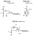
- FIG.3A shows a third example of a conventional charge injection circuit.
- the charge injection circuit has a photo-voltaic element 11, a MOS type FET 12, a load resistance R L and a capacitor C for providing an A.C. coupling between a gate of the FET 12 and a node connecting a cathode of the photo-voltaic element 11 and the load resistance R L .
- This charge injection circuit is referred to as a "gate coupling type" because an A.C. component of an output voltage of the photo-voltaic element 11 is applied to the gate of the FET 12.
- a source of the FET 12 is grounded, and a drain of the FET 12 is connected to a signal processing circuit (not shown) such as a CCD to which the charge is to be injected.
- FIG.3B shows an equivalent circuit of a circuit portion of the charge injection circuit shown in FIG.3A including the photo-voltaic element 11 and the load resistance R L .
- a current source 14 of the photo-voltaic element 11 generates a photocurrent I P when the photo-voltaic element 11 receives an infrared light.
- the current source 14 is connected in parallel to the internal resistance R0 thereof and is connected in series to the load resistance R L .
- Vdd denotes a power source voltage
- V OUT denotes an output voltage supplied to the gate of the FET 12.
- the photo-voltaic element 11 generates the photocurrent I P depending on the received infrared light and the output voltage V OUT described by the formula (4) is obtained from the cathode of the photo-voltaic element 11.
- the output voltage V OUT described by the formula (4) is obtained from the cathode of the photo-voltaic element 11.
- only an A.C. component of the output voltage V OUT is applied to the gate of the FET 12 due to the provision of the capacitor C, and as a result the drain current flowing through the FET 12 is injected to the signal processing circuit.
- the charge (current) injected to the signal processing circuit corresponds to the A.C. component of the output voltage V OUT of the photo-voltaic element 11.
- FIG.4 shows a fourth example of a conventional charge injection circuit.
- the charge injection circuit shown in FIG.4 has a negative feedback amplifier 5 for applying the source potential of the FET 2 to the gate of the FET 2.
- a current I2 flowing between the drain and source of the FET 2 can be described by the following formula (5), where I P denotes the photocurrent flowing through the photo-voltaic element 1, -B (B >> 1) denotes the gain of the negative feedback amplifier 5, R0 denotes the internal resistance of the photo-voltaic element 1 and gm denotes the mutual conductance of the FET 2.
- I2 [(1 + B) ⁇ gm ⁇ R0 ⁇ I P ]/[1 + (1 + B) ⁇ gm ⁇ R0]
- the injection efficiency is improved compared to the charge injection circuit shown in FIG.1A because the conductance gm is effectively improved to (1 + B) times that of the charge injection circuit shown in FIG.1A.
- the conductance gm is effectively improved to (1 + B) times that of the charge injection circuit shown in FIG.1A.
- FIG.5A shows a first embodiment of the charge injection circuit according to the present invention.
- a cathode of a photo-voltaic element 21 is directly connected to a source diffusion layer of a MOS type FET 22.
- a gate of the FET 22 is applied with a gate voltage Vg through an input terminal 23.
- a drain of the FET 22 is connected to a signal processing circuit (not shown) such as a CCD to which the charge is to be injected.
- an impedance conversion circuit 25 is connected between the cathode and anode of the photo-voltaic element 21.
- the impedance conversion circuit 25 has a gain A which is less than or equal to one. Hence, a source potential V S of the FET 22 is fed back to a substrate potential (anode) of the photo-voltaic element 21 through the impedance conversion circuit 25.
- FIG.5B shows an A.C. equivalent circuit diagram of the direct injection type charge injection circuit shown in FIG.5A.
- a current source 24 of the photo-voltaic element 21 generates a photocurrent I P when the photo-voltaic element 21 receives an infrared light.
- the photocurrent I P is divided by an internal resistance R0 of the photo-voltaic element 21 and an impedance 1/gm which is an inverse number of a mutual conductance gm of the FET 22.
- a voltage source 26 corresponds to a voltage AV S which is obtained by a positive feedback of the source potential V S of the FET 22 to the substrate potential of the photo-voltaic element 21.
- FIG.6 shows an embodiment of the circuit construction of the first embodiment.
- the impedance conversion circuit 25 has a MOS type FET 30.
- a gate of the FET 30 is connected to the source of the FET 22 and to the cathode of the photo-voltaic element 21.
- a MOS type FET 31 acts as a load on the FET 30 and a gate and a source of the FET 31 are connected to each other.
- a drain of the FET 31 is connected to a node connecting a source of the FET 30 and the photo-voltaic element 21.
- V DD and V SS denote respective power source voltages to the drain of the FET 30 and the source of the FET 31.
- FIG.7 shows a cross sectional view of the construction of an essential part of the circuit shown in FIG.6.
- the photo-voltaic element 21 has a p-type substrate 32, an n+-type diffusion layer 33 formed in the p-type substrate 32, and an insulator layer 34 formed on the p-type substrate 32.
- the p-type substrate 32 is made of indium antimony (InSb), lead tin telluride (PbSnTe), mercury cadmium telluride (HgCdTe) or the like.
- the insulator layer 34 is made of silicon dioxide (SiO2), zinc sulfide (ZnS) or the like.
- n+-type diffusion layers 38, 39 and 40 are formed within the p-type well 36.
- n+-type diffusion layer 41 is formed within the other p-type well 37.
- the n+-type diffusion layer 41 constitutes a source region of the FET 22 and also constitutes the input diode together with the p-type well 37.
- gate electrodes 43 and 44 made of polysilicon or the like, an input gate electrode 45, a storage gate 46, an electrode 47 which constitutes a part of the signal processing circuit (CCD) are thereafter formed on the n-type Si substrate 35.
- the drain of the FET 22 corresponds to the region of the p-type well 37 immediately below the storage gate 46, and the gate of the FET 22 corresponds to the input gate electrode 45.
- the drain of the FET 30 corresponds to the n+-type diffusion layer 38. Because the source of the FET 30 and the drain of the FET 31 always have the same potential, the n+-type diffusion layer 39 is used in common as the source of the FET 30 and the drain of the FET 31.
- the source of the FET 31 corresponds to the n+-type diffusion layer 40.
- the photocurrent generated when the photo-voltaic element 21 receives the infrared light is supplied from the n+-type diffusion layer 33 to the n+-type diffusion layer 41.
- the photocurrent supplied to the n+-type diffusion layer 41 then passes through the region of the p-type well 37 immediately below the input gate electrode 45 and is stored as a signal charge in the potential well of the region of the p-type well 37 immediately below the storage gate 46.
- the n+-type diffusion layer 41, the potential well immediately below the electrode 46 and the gate electrode 45 substantially constitute the FET 22.
- the signal charge is thereafter transferred to the signal processing circuit (CCD).
- the source potential V S at the n+-type diffusion layer 41 is fed back to the p-type substrate 32 of the photo-voltaic element 21 through the gate electrode 43, the n+-type diffusion layer 39 and a connection line 48. Accordingly, the injection efficiency of this embodiment is greatly improved compared to that of the conventional charge injection circuit.
- the FETs 30 and 31 constitute a source follower and the gain A of the impedance conversion circuit 25 is approximately 0.9.
- the value of the internal resistance R0 is improved to over ten times that of the conventional charge injection circuit.
- FIG.8 shows a voltage versus current characteristic for explaining the injection efficiency.
- the source potential V S and the current of the photo-voltaic element 21 have a relationship indicated by a solid line I in FIG.8.
- a D.C. current I B is generated by the background light and the like.
- the input gate voltage Vg is a predetermined constant value
- the input source potential V S of the FET 22 and the current of the photo-voltaic element 21 have a relationship indicated by a solid line II in FIG.8.
- An intersection C1 of the characteristics (curves) I and II is the operating point for the case where there is no subject of detection.
- the source potential V S and the current of the photo-voltaic element have a relationship indicated by a solid line III in FIG.8. It can be seen that the characteristic III is obtained by shifting the characteristic I by the quantity of the photocurrent I P parallel with respect to the current axis.
- the operating point in this case is located at a position C2 and the injection current is increased by the quantity of the current I22 compared to the operating point C1 for the case where there is no subject of detection.
- the source potential V S and the current of the photo-voltaic element 21 have a relationship indicated by a one-dot chain line IV in FIG.8. It can be seen that the source potential V S is reduced compared to that of the conventional charge injection circuit, and the substrate potential of the photo-voltaic element 21 is also shifted to a smaller value at a certain gain.
- the operating point in this embodiment is thus located at a position C3, and the injection current is I P ( > I22) and large compared to the case where there is no incoming infrared light.
- the operating point is varied depending on the photocurrent I P by feeding back the source potential V S of the FET 22 to the substrate potential of the photo-voltaic element 21. Further, according to this embodiment, the injection efficiency is greatly improved compared to that of the conventional charge injection circuit.
- a lowpass filter 27 is connected between the impedance conversion circuit 25 and the anode of the photo-voltaic element 21.
- the source potential V S of the FET 22 is fed back to the substrate potential of the photo-voltaic element 21 through the impedance conversion circuit 25 and the lowpass filter 27 which is provided in the feedback path.
- the lowpass filter 27 reduces the feedback gain in the high frequency region to reduce the injection efficiency in the high frequency region and accordingly improve the S/N ratio of the photo-voltaic element 21.
- the first embodiment shown in FIG.5A has the high injection efficiency also with respect to a white noise which is the dominant noise in the ideal photo-voltaic element 21. For this reason, the sensitivity of the infrared detector element is improved and the S/N ratio is improved with respect to external noise, but the first embodiment does not contribute to the improvement of the S/N ratio of the photo-voltaic element 21.
- the white noise is added and amplified by the aliasing effect when the multiplexing takes place in for example a horizontal transfer register within the signal processing circuit.
- the white noise greatly deteriorates the S/N ratio of an output video signal of the horizontal transfer register.
- the lowpass filter 27 reduces the injection efficiency of the high frequency component.
- the internal resistance R0 greatly decreases when the photo-voltaic element 21 has a long cutoff wavelength or the photo-voltaic element 21 operates under a high temperature, and thus, gm ⁇ R0 ⁇ 1 in such a case.
- A 0.9
- FIG.10 shows an embodiment of the circuit construction of the second embodiment.
- those parts which are the same as those corresponding parts in FIG.6 are designated by the same reference numerals, and a description thereof will be omitted.
- the lowpass filter 27 which has a filter characteristic shown in FIG.11 with respect to the voltage obtained from the source of the FET 30 is constituted by the capacitor C11, the impedance of the FET 31 and the impedance of the FET 30 of the source follower.
- FIG.12 shows another embodiment of the circuit construction of the second embodiment.
- those parts which are the same as those corresponding parts in FIG.10 are designated by the same reference numerals, and a description thereof will be omitted.
- one end of a resistor R1 is connected to the source of the FET 30 and the drain of the FET 31, while the other end of the resistor R1 is connected to the capacitor C11 and the substrate of the photo-voltaic element 21.
- the resistor R1 restricts the frequency characteristic of the lowpass filter 27.
- the lowpass filter characteristic can be realized without the use of the resistor R1, but the terminal voltage of the capacitor C11 stabilizes when the resistor R1 is used.
- the source potential V S is fed back to the substrate potential of the photo-voltaic element 21 through the lowpass filter 27.
- the impedance conversion circuit 25 is not limited to the source follower and it is possible to use an emitter follower, for example.
- the frequency characteristic in the high frequency region may be intentionally deteriorated by determining the various constants when designing the lowpass filter 27.
- the FET 22, the impedance conversion circuit 25, the signal processing circuit and the lowpass filter 27 may be formed on a single substrate.
- the first and second embodiments use the MOS type FET for the FET 22, but it is of course possible to use a junction type FET.
- an infrared detector has a plurality of photo-voltaic elements arranged in an array, and currents generated in parallel are supplied to a signal processing circuit (CCD) through corresponding MOS transistors. A signal multiplexing takes place in the signal processing circuit and a serial signal is obtained from the signal processing circuit.
- CCD signal processing circuit
- a signal multiplexing takes place in the signal processing circuit and a serial signal is obtained from the signal processing circuit.
- the ohmic contact with the substrate must be made independently for each of the photo-voltaic elements 21 because the positive feedback is independently made to the substrate from each of the photo-voltaic elements 21. For this reason, it is necessary to electrically isolate the photo-voltaic elements 21 and connect the substrate of each photo-voltaic element 21 to the impedance conversion circuit 25.
- the ohmic contact with the substrate is formed within the diffusion length of the minority carriers within a p-type layer from a pn junction interface of the photo-voltaic element 21, the surface recombination velocity becomes large and a dark current increases.
- FIGS.13A and 13B are a cross sectional view and a plan view respectively showing a third embodiment of the charge injection circuit according to the present invention.
- those parts which are the same as those corresponding parts in FIG.5A are designated by the same reference numerals, and a description thereof will be omitted.
- IR denotes the incoming infrared light.
- a semiconductor substrate 56 made of HgCdTe, for example, is provided on an insulator body 55 made of CdTe, for example.
- the semiconductor substrate 56 is provided on the insulator body 55 with a sufficiently large light receiving area.
- a pn+ junction of a p-type layer 56p and an n+-type layer 56n is formed by an ion implantation, and an epitaxial layer or a bulk crystal film is used.
- a contact portion 57 makes contact with the n+-type layer 56n of the semiconductor substrate 56 and is also connected to a node connecting one end of the impedance conversion circuit 25 and the source of the FET 22.
- An ohmic contact portion 58 makes contact with the p-type layer 56p of the semiconductor substrate 56 and is also connected to the other end of the impedance conversion circuit 25.
- a protection layer 59 made of zinc sulfide (ZnS), for examples is formed on the semiconductor substrate 56.
- the photo-voltaic element 21 is constituted by the semiconductor substrate 56, the contact portions 57 and 58, and the protection layer 59.
- the contact portion 58 is formed at a portion located the diffusion length or more of the minority carriers within the p-type layer 56p away from a pn+ junction interface 56a of the semiconductor substrate 56.
- L denotes a distance between the pn+ junction interface 56a and the ohmic contact portion 58 which is the diffusion length or more away from the pn+ junction interface 56a.
- FIG.14 shows the photo-voltaic element 21, the FET 22 and the impedance conversion circuit 25 arranged in an array.
- photo-voltaic elements 211 through 213, FETs 221 through 223, and impedance conversion circuits 251 through 253 are shown.
- the FETs 221 through 223, the impedance conversion circuits 251 through 253, and a CCD 60 are provided on a substrate 61 made of Si, for example.
- the photo-voltaic elements 211 through 213 are provided on the insulator body 55.
- the photo-voltaic elements 211 through 213 are electrically isolated by a process such as ion milling.
- the photo-voltaic elements 211 through 213 are connected to the FETs 221 through 223 and the impedance conversion circuits 251 through 253 by a wire bonding or the like.
- An output serial signal of the CCD 60 is obtained from a terminal 63 through an amplifier 62.
- FIGS.15A and 15B are a cross sectional view and a perspective view respectively showing a fourth embodiment of the charge injection circuit according to the present invention.
- FIGS.15A and 15B those parts which are essentially the same as those corresponding parts in FIGS.13A and 13B are designated by the same reference numerals, and a description thereof will be omitted.
- a semiconductor substrate 65 has a p-type layer 65p and an n+-type layer 65n, and the p-type layer 65p has a p+-type layer 65pp which is doped to a p+-type and has a high carrier density.
- the contact portion 57 makes contact with the n+-type layer 65n, and the ohmic contact portion 58 makes contact with the p+-type layer 65pp.
- the ohmic contact portion 58 is located at a portion within the diffusion length of the minority carriers within the p-type layer 65 away from the pn+ junction interface 56a. The arrangement of the array becomes substantially the same as that shown in FIG.14.
- the p+-type layer 65pp has an electrically reflecting state with respect to the minority carriers within the p-type layer 65p and suppresses the generation of the minority carriers.
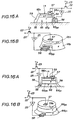
- FIGS.16A and 16B are a cross sectional view and a perspective view respectively showing a fifth embodiment of the charge injection circuit according to the present invention.
- those parts which are essentially the same as those corresponding parts in FIGS.13A and 13B are designated by the same reference numerals, and a description thereof will be omitted.
- a semiconductor substrate 66 has a p-type layer 66p1, a p-type layer 66p2, and a n+-type layer 66n.
- the p-type layer 66p1 is made of a semiconductor having a wide band gap
- the p-type layer 66p2 and the n+-type layer 66n are made of a semiconductor having a narrow band gap thereby constituting a diode.
- the contact portion 57 makes contact with the n+-type layer 66n
- the ohmic contact portion 58 makes contact with the p-type layer 66p1.
- the structure shown in FIGS.16A and 16B is obtained by forming the p-type layer 66p2 made of the narrow band gap semiconductor on the p-type layer 66p1 which is an epitaxial layer. Then, the n+-type layer 66n is formed on the p-type layer 66p2, and the n+pp junction is formed by a mesa etching. The arrangement of the array becomes substantially the same as that shown in FIG.14.
- the ohmic contact portion 58 is substantially located at a portion the diffusion length or more of the minority carriers away from the pn+ junction interface, and it is thus possible to reduce the dark current.
- FIG.17 is a perspective view showing a sixth embodiment of the charge injection circuit according to the present invention.
- those parts which are essentially the same as those corresponding parts in FIGS.13A and 13B are designated by the same reference numerals, and a description thereof will be omitted.
- the diode portion has a planar structure.
- a semiconductor substrate 67 has a p-type layer 67p and an n+-type layer 67n, and a pn+ junction interface is exposed at the wafer.
- the substrate ohmic contact portion 58 is located the diffusion length or more of the minority carriers within the p-type layer 67p from the pn+ junction interface of the semiconductor substrate 67. The effects obtainable in this embodiment are the same as those obtainable in the third through fifth embodiments described before.
- the charge injection circuit When arranging the photo-voltaic elements in the array or matrix arrangement, the charge injection circuit must be provided for each photo-voltaic element. As a result, the structure of the infrared detector becomes extremely complex. Next, a description will be given on embodiments in which the structure of the infrared detector is simplified.
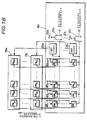
- FIG.18 is a block diagram for explaining the operating principle of a seventh embodiment of the charge injection circuit according to the present invention which is a scan type charge injection circuit.
- m x n photo-voltaic elements 7811 through 78 mn are arranged in an array or matrix arrangement.
- n photo-voltaic elements arranged in a line direction, that is, a line address direction, and there are m photo-voltaic elements arranged in a direction perpendicular to the line address direction.
- a substrate 80 is provided independently of the detector element substrates 791 through 79 n .
- MOS type FETs 221 through 22 n which constitute input gates provided for each column perpendicular to the line address direction, impedance circuits 251 through 25 n , address switches SW11 through SW mn provided in 1:1 correspondence with the photo-voltaic elements 7811 through 78 mn , and signal processing circuits (not shown) are provided on the substrate 80. Terminals 231 through 23 n are connected to the corresponding gates of the FETs 221 through 22 n .
- the m photo-voltaic elements 78 1j through 78 mj provided on the detector element substrate 79 j are coupled in common to a source of the FET 22 j through the respective address switches SW11 through SW mn .
- the source of the FET 22 j is coupled to the detector element substrate 79 j through the corresponding impedance conversion circuit 25 j .
- the n address switches SW11 through SW mn are controlled responsive to switching signals applied to terminals 831 through 83 m so that the address switches of the same line address are simultaneously turned ON and the address switches are sequentially turned ON in the sequence of the line address.
- the FETs 221 through 22 n are sequentially turned ON within the time in which the n address switches of the same line address are simultaneously turned ON.
- the m photo-voltaic elements 7811 through 78 m1 are respectively connected to the m address switches SW11 through SW m1 .
- the address switches SW11 through SW m1 are sequentially turned ON based on the switching signals from the terminals 831 through 83 m and it is impossible that two or more address switches are turned ON simultaneously.
- the photocurrent (charge) from only one of the photo-voltaic elements 7811 through 78 m1 is obtained through a corresponding one of the address switches SW11 through SW m1 which is turned ON and is supplied to the source of the FET 221.
- the source potential of the FET 221 is only due to the photocurrent from one of the m photo-voltaic elements 7811 through 78 m1 provided on the common detector element substrate 791, and the photocurrents from two or more photo-voltaic elements will not be mixed. For this reason, it is possible to accurately inject the charge from one photo-voltaic element, and the injection efficiency is improved as in the case of the first embodiment described before in conjunction with FIGS.5A and 5B by making a positive feedback to the detector element substrate 791 through the impedance conversion circuit 251.
- the injection of the charge from one photo-voltaic element and the positive feedback to the detector element substrate are carried out for every m photo-voltaic elements and m address switches arranged perpendicularly to the line address direction by using in common the FETs 221 through 22 n , the impedance conversion circuits 251 through 25 n and the detector element substrates 791 through 79 n .
- FIG.19 shows an embodiment of an essential part of the seventh embodiment shown in FIG.18.
- those parts which are the same as those corresponding parts in FIG.18 are designated by the same reference numerals, and a description thereof will be omitted.
- the circuit construction is only shown for one column perpendicular to the line address direction.
- the cathodes of the photo-voltaic elements 7811 through 78 m1 are respectively coupled to the input side of the impedance conversion circuit 251 through sources and drains of MOS type FETS 8411 through 84 m1 which respectively correspond to the address switches SW11 rough SW m1 .
- the impedance conversion circuit 251 is a buffer amplifier (non-inverting amplifier) having the gain A which is less than or equal to one.
- the impedance conversion circuit 251 is made up of a source follower, an emitter follower, or a voltage follower using an operational amplifier.
- the output side of the impedance conversion circuit 251 is connected to the detector element substrate 791.
- one FET which is ON receives the photocurrent from one selected photo-voltaic element connected thereto, and the received photocurrent is passed through the source and drain of the FET which is ON and supplied to the source of the FET 221 which constitutes the input gate.
- the source potential of the FET 221 is positively fed back to the anodes of the m photo-voltaic elements 7811 through 78 m1 including the one selected photo-voltaic element through the impedance conversion circuit 251. Accordingly, the injection efficiency of the charge injection circuit is improved.
- FIG.20 shows an embodiment of the construction of an essential part of the seventh embodiment shown in FIG.18.
- FIG.20 shows the construction of the detector element substrates 791 and 792, and the illustration of the other detector element substrates 793 through 79 n and the substrate 80 is omitted.
- An insulator substrate 87 is made of sapphire, gallium arsenide (GaAs), cadmium telluride (CdTe) or the like.
- a semiconductor film made of InSb, HgCdTe or the like is formed on the insulator substrate 87 and patterned into bands to isolate the columns to form the detector element substrates 791 and 792.
- Photodiodes 8911 through 89 m1 which correspond to the photo-voltaic elements 7811 through 78 m1 are formed on the detector element substrate 791. Similarly, photodiodes 8912 through 89 m2 which correspond to the photo-voltaic elements 7812 through 78 m2 are formed on the detector element substrate 792. Input terminals 901 and 902 respectively receive the signals from the impedance conversion circuits 251 and 252, and the source potentials of the FETs 221 and 222 are positively fed back.
- FIG.21 shows an embodiment of the construction of another essential part of the seventh embodiment shown in FIG.18.
- FIG.21 shows the detector element substrate 791 shown in FIG.20 in a side view together with the substrate 80.
- the detector element substrate 791 is a p-type substrate made of InSb, HgCdTe or the like, and n+-type regions 9111 through 91 m1 are formed in the detector element substrate 791 to constitute the photodiodes 8911 through 89 m1 which respectively correspond to the photo-voltaic elements 7811 through 78 m1 .
- a thin film 92 made of SiO2, ZnS or the like is formed on the detector element substrate 791 and contact holes are formed in the thin film 92.
- Bump electrodes 93 made of indium (In) or the like are formed in the contact holes and connect the n+-type regions 9111 through 91 m1 to the sources of the corresponding FETs 8411 through 84 m1 formed on the substrate 80.
- the output terminal of the impedance conversion circuit 251 provided on the substrate 80 is connected to the detector element substrate 791 through a bump electrode 94.
- the infrared light is irradiated downwardly in FIG.21 onto the back surface of the insulator substrate 87 to generate the minority carriers.
- FIG.21 only the FETs 8411 through 84 m1 , the impedance conversion circuit 251 and the FET 221 amounting to one column are shown on the substrate 80. However, there actually are n columns of such circuits provided in parallel.
- FIG.22 shows another embodiment of the construction of an essential part of the seventh embodiment shown in FIG.18.
- those parts which are essentially the same as those corresponding parts in FIG.20 are designated by the same reference numerals, and a description thereof will be omitted.
- the circuits such as the FETs 221 and 8411 through 84 m1 , and the impedance conversion circuit 251 are provided on the substrate 80 which is made of Si, for example, and such circuits amounting to n columns are provided on the substrate 80.
- the detector element substrates 791 through 79 n (only 791 shown in FIG.22) are adhered on the substrate 80 to constitute the scanning type charge injection circuit.
- An infrared detecting material such as InSb and HgCdTe is used for the detector element substrates 791 through 79 n .
- the photodiodes 8911 through 89 m1 may be formed before or after the detector element substrate 791 is adhered on the substrate 80. In this embodiment, the infrared light is irradiated downwardly in FIG.22 from above the detector element substrate 791 and the like.
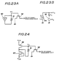
- FIG.23A is a circuit diagram showing an eighth embodiment of the charge injection circuit according to the present invention
- FIG.23B is an A.C. equivalent circuit diagram of the charge injection circuit shown in FIG.23A excluding the FET.
- a potential at a node connecting a photo-voltaic element 91 and a gate of a FET 92 is positively fed back to a substrate potential of the photo-voltaic element 91 through an impedance conversion circuit 93 having a gain A which is less than or equal to one.
- a current source 94 generates a photocurrent I P when the photo-voltaic element 91 receives an infrared light.
- the photocurrent I P is dependent on a quantity of the received infrared light.
- a voltage source 95 corresponds to a voltage AV G which is obtained by a positive feedback of a potential V G at the node connecting the photo-voltaic element 91 and the gate of the FET 92 to the substrate potential of the photo-voltaic element 91 through the impedance conversion circuit 93, where A is less than or equal to one.
- the internal resistance R0 of the photo-voltaic element 91 is connected in series with the voltage source 95.
- a node connecting the internal resistance R0 and the current source 94 is connected to the gate of the FET 92.
- no current flows to the gate of the FET 92, and the photocurrent I P flows through the series circuit of the internal resistance R0 and the voltage source 94 without being divided. Accordingly, the gate voltage (open voltage) V G can be described by the following formula (11).
- V G (I P ⁇ R0)/(1 - A)
- the open voltage V G is 1/(1 - A) times the open voltage I P ⁇ R0 of the conventional charge injection circuit described before in conjunction with FIGS.3A and 3B. Since the gain A is less than or equal to one, it may be seen that the open voltage V G is amplified by 1/(1 - A).
- FIG.24 is a circuit diagram showing an embodiment of the circuit construction of the eighth embodiment shown in FIG.23A.
- those parts which are the same as those corresponding parts in FIG.23A are designated by the same reference numerals, and a description thereof will be omitted.
- a gate of a MOS type FET 96 is connected to the node connecting the photo-voltaic element 91 and the gate of the FET 92.
- a source of the FET 96 is connected to the anode (substrate) of the photo-voltaic element 91 and a drain of a MOS type FET 97.
- the FET 97 acts as a load on the FET 96 and the gate and a source of the FET 97 are connected to each other.
- the FETs 96 and 97 constitute a source follower corresponding to the impedance conversion circuit 93.
- Vdd and Vss denote respective power source voltages to the drain of the FET 96 and the source of the FET 97.
- FIG.25 is a cross sectional view showing the construction of an essential part of the circuit shown in FIG.24.
- the photo-voltaic element 91 has a p-type substrate 110, an n+-type diffusion layer 111 formed in the p-type substrate 110, and an insulator layer 112 formed on the p-type substrate 110.
- the p-type substrate 110 is made of InSb, PbSnTe, HgCdTe or the like.
- the insulator layer 112 is made of SiO2, ZnS or the like.
- n+-type diffusion layers 116, 117 and 118 are formed within the p-type well 114.
- an n+-type diffusion layer 119 is formed within the other p-type well 115.
- the n+-type diffusion layer 119 constitutes a source region of the FET 92 and also constitutes the input diode together with the p-type well 115.
- gate electrodes 121 and 122 made of polysilicon and the like, an input gate electrode 123, a storage gate 124, an electrode 125 which constitutes a part of the signal processing circuit (CCD) are thereafter formed on the n-type Si substrate 113.
- the drain of the FET 92 corresponds to the region of the p-type well 115 immediately below the storage gate 124, and the gate of the FET 92 corresponds to the input gate electrode 123.
- the drain of the FET 96 corresponds to the n+ diffusion layer 116. Because the source of the FET 96 and the drain of the FET 97 always have the same potential, the n+-type diffusion layer 117 is used in common as the source of the FET 96 and the drain of the FET 97.
- the source of the FET 97 corresponds to the n+-type diffusion layer 118.
- the open voltage V G determined by a product of the photocurrent generated when the photo-voltaic element 91 receives the infrared light and the internal resistance R0 of the photo-voltaic element 91 is supplied from the n+-type diffusion layer 111 to the gate electrode 121 which corresponds to the gate of the FET 96.
- the open voltage V G is subject to the impedance conversion in the FET 96 which is made up of the gate electrode 121, the oxide layer 120, the n+-type diffusion layers 116 and 117, the p-type well 114, and the Si substrate 113. Then, the open voltage V G subject to the impedance conversion is positively fed back to the substrate 110 through the n+-type diffusion layer 117.
- the open voltage V G which is amplified in this manner is applied to the gate electrode 123 through the n+-type diffusion layer 111, and then passes through the region of the p-type well 115 immediately below the input gate electrode 123 to store a signal charge in the potential well of the region of the p-type well 115 immediately below the storage gate 124.
- the gain A of the source follower constituted by the FETs 96 and 97 can easily be set in the range of 0.9.
- the open voltage V G can be improved to approximately ten times that obtained in the conventional charge injection circuit described before in conjunction with FIGS.3A and 3B.
- the drain current of the FET 92 becomes large and the signal quantity becomes large while the noise is approximately constant, thereby making it possible to considerably improve the S/N ratio.
- the impedance conversion circuit 93 is not limited to the source follower, and other circuits having a gain close to one may be used. Examples of such circuits are the emitter follower having a greater current driving capability than the source follower, and the operational amplifier.
- the FET 92, the impedance conversion circuit 93 and the signal processing circuit may be provided on the same substrate (not shown).
- the FET 92 is not limited to the MOS type FET, and a junction type FET, for example, may be used for the FET 92.
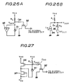
- FIG.26A is a circuit diagram showing a ninth embodiment of the charge injection circuit according to the present invention
- FIG.26B is an A.C. equivalent circuit diagram of the input circuit portion of the charge injection circuit shown in FIG.26A.
- FIGS.26A and 26B those parts which are essentially the same as those corresponding parts in FIGS.23A and 23B are designated by the same reference numerals, and a description thereof will be omitted.
- the output voltage V OUT of the photo-voltaic element 91 which is biased through a load resistance R L is positively fed back to the substrate potential of the photo-voltaic element 91 through the impedance conversion circuit 93 having the gain A which is less than or equal to one, as shown in FIG.26A.
- a capacitor C20 is connected between the gate of the FET 92 and a node connecting the photo-voltaic element 91, the impedance conversion circuit 93 and the load resistance R L .
- the voltage source 95 corresponds to the voltage AV OUT which is obtained by a positive feedback of the output voltage V OUT to the substrate potential of the photo-voltaic element 91 through the impedance conversion circuit 93, where A is less than or equal to one.
- the voltage source 95 is coupled to the input terminal of the power source voltage Vdd through the internal resistance R0 of the photo-voltaic element 91 and the load resistance R L which are connected in series. A series circuit of the voltage source 95 and the internal resistance R0 is connected in parallel to the current source 94.
- the gain A of the impedance conversion circuit 93 is less than or equal to one, the internal resistance R0 is in effect multiplied by 1/(1 - A), and it is possible to make the voltage supplied to the gate of the FET 92 large even when the value of the load resistance R L is large.
- FIG.27 is a circuit diagram showing an embodiment of the circuit construction of the ninth embodiment shown in FIG.26A.
- those parts which are the same as those corresponding parts in FIGS.24 and 26A are designated by the same reference numerals, and a description thereof will be omitted.
- the gate of a MOS type FET 96 is connected to the node connecting the photo-voltaic element 91, the load resistance R L and the capacitor C20.
- the source of the FET 96 is connected to the anode (substrate) of the photo-voltaic element 91 and the drain of the FET 97.
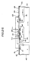
- FIG.28 is a cross sectional view showing the construction of an essential part of the circuit shown in FIG.27.
- those parts which are essentially the same as those corresponding parts in FIG.25 are designated by the same reference numerals, and a description thereof will be omitted.
- a non-doped polysilicon layer 126 is formed on the oxide layer 120 to constitute the load resistance R L .
- a polysilicon layer 127, an oxide layer 128 made of SiO2 or the like and a polysilicon layer 129 are sequentially stacked to constitute the capacitor C20.
- the output voltage V OUT determined by the photocurrent generated when the photo-voltaic element 91 receives the infrared light and the internal resistance R0 of the photo-voltaic element 91 is supplied from the n+-type diffusion layer 111 to the gate electrode 121 which corresponds to the gate of the FET 96.
- the output voltage V OUT is subject to the impedance conversion in the FET 96 which is made up of the gate electrode 121, the oxide layer 120, the n+-type diffusion layers 116 and 117, the p-type well 114, and the Si substrate 113. Then, the output voltage V OUT subject to the impedance conversion is positively fed back to the substrate 110 through the n+-type diffusion layer 117.
- the output voltage V OUT which is amplified in this manner and described by the formula (14) is obtained from the n+-type diffusion layer 111.
- the obtained output voltage V OUT is applied to the gate electrode 123 through the capacitor C20 which passes only the A.C. component, and is then passed through the region of the p-type well 115 immediately below the input gate electrode 123 to store a signal charge in the potential well of the region of the p-type well 115 immediately below the storage gate 124.
- the gain A of the source follower constituted by the FETs 96 and 97 can easily be set in the range of 0.9.
- the output voltage V OUT can be improved to approximately ten times that obtained in the conventional charge injection circuit described before.
- the drain current of the FET 92 becomes large and the signal quantity becomes large while the noise is approximately constant, thereby making it possible to considerably improve the S/N ratio.
- the impedance conversion circuit 93 is not limited to the source follower, and other circuits having a gain close to one may be used.
- the load resistance R L may be formed by changing the width-to-length ratio of a MOS type FET instead of using the polysilicon layer 126.
- the FET 92 is not limited to the MOS type FET, and a junction type FET, for example, may be used for the FET 92.
- the gain -B of the negative feedback amplifier 5 can be set to approximately 10 when the stable operation and power consumption are considered.
- the injection efficiency is only in the order of ten times that of the conventional charge injection circuit not having the negative feedback.
- the impedance conversion circuit 25 is constituted by a source follower and the gain A thereof is approximately 0.9.
- the injection efficiency is only in the order of ten times that of the conventional charge injection circuit not having the negative feedback or the impedance conversion circuit.
- FIG.29 shows a tenth embodiment of the charge injection circuit according to the present invention.
- those parts which are essentially the same as those corresponding parts in FIG.5A are designated by the same reference numerals, and a description thereof will be omitted.
- a negative feedback amplifier 130 having a gain -B is provided between the cathode of the photo-voltaic element 21 and the gate of the FET 22.
- the source potential of the FET 22 is positively fed back to the anode (substrate potential) of the photo-voltaic element 21 through the impedance conversion circuit 25 having the gain A which is less than or equal to one, while the source potential of the FET 22 is also negatively fed back to the gate of the FET 22 through the negative feedback amplifier 130 which has the gain -B.
- FIG.30 shows only the gate feedback portion of the charge injection circuit shown in FIG.29.
- I I ds ⁇ exp[q(Vg - V S )/nkT]
- the mutual conductance gm becomes (1 + B) times in the weak inversion state by the negative feedback to the gate of the FET 22.
- the gain A of the impedance conversion circuit 25 is 0.9 and the gain -B of the negative feedback amplifier 130 is -10, it may be seen from the formula (24) that the product gmR0 is greatly improved to (1 + B)/(1 - A) times, that is, 110 times that of the conventional charge injection circuit shown in FIG.1A.
- FIG.32 is a circuit diagram showing an embodiment of the circuit construction of the tenth embodiment shown in FIG.29.
- those parts which are the same as those corresponding parts in FIG.6 are designated by the same reference numerals, and a description thereof will be omitted.
- a MOS type FET 135 constitutes an inverting amplifier corresponding to the negative feedback amplifier 130.
- a gate of the FET 135 is connected to a node connecting the source of the FET 22, the cathode of the photo-voltaic element 21 and the gate of the FET 30.
- a drain of the FET 135 is connected to a source of a MOS type FET 136 and the gate of the FET 22.
- the FET 136 acts as a load on the FET 135 and the gate and a drain of the FET 136 are connected to each other.
- V S1 and V S2 denote respective power source voltages to the source of the FET 31 and the source of the FET 135, and V D1 and V D2 denote respective power source voltages to the drain of the FET 30 and the drain of the FET 136.
- the gain A of 0.9 can easily be realized by the source follower constituted by the FETs 30 and 31, and the gain -B of -10 can easily be realized by the inverting amplifier constituted by the FETs 135 and 136.
- FIG.33 is a cross sectional view showing the construction of an essential part of the circuit shown in FIG.32.
- those parts which are essentially the same as those corresponding parts in FIG.7 are designated by the same reference numerals, and a description thereof will be omitted.
- a p-type well 143 is formed in the n-type Si substrate 35.
- n+-type diffusion layers 148, 149 and 150 are formed within the p-type well 143.
- the oxide layer 42 made of SiO2, for example, is formed by a known means on the n-type Si substrate 35 which is already formed with the regions described above.
- Gate electrodes 155 and 156 made of polysilicon and the like are also formed on the n-type Si substrate 35 after the formation of the oxide layer 42.
- the drain of the FET 136 corresponds to the n+-type diffusion layer 148. Because the source of the FET 136 and the drain of the FET 135 always have the same potential, the n+-type diffusion layer 149 is used in common as the source of the FET 136 and the drain of the FET 135. The source of the FET 135 corresponds to the n+-type diffusion layer 150.
- the photocurrent generated when the photo-voltaic element 21 receives the infrared light is supplied from the n+-type diffusion layer 33 to the n+-type diffusion layer 41.
- the photocurrent supplied to the n+-type diffusion layer 41 then passes through the region of the p-type well 37 immediately below the input gate electrode 45 and is stored as a signal charge in the potential well of the region of the p-type well 37 immediately below the storage gate 46.
- the n+-type diffusion layer 41, the potential well immediately below the gate electrode 25 and the electrode 26 substantially constitute the FET 22.
- the signal charge is thereafter transferred to the signal processing circuit (CCD).
- the source potential V S at the n+-type diffusion layer 41 is fed back to the p-type substrate 32 of the photo-voltaic element 21 through the gate electrode 43, the n+-type diffusion layer 39 and the connection line 48. Furthermore, the source potential V S is fed back to the input gate electrode 45 through the gate electrode 156, the n+-type diffusion layer 149 and a connection line 158.
- the injection efficiency is in the range of 9%. But according to this embodiment, the injection efficiency is approximately 92% which is ten or more times that obtainable in the conventional charge injection circuit, as may be seen from the coefficient of I P in the formula (24).
- the infrared detector can detect infrared light having a long wavelength and the infrared detector can be operated under a high temperature. Further, the effective product gmR0 can be improved to 100 or more times that of the conventional charge injection circuit.
- bipolar transistors in place of the MOS type FETs.
- resistors may be used in place of the MOS type FETs which act as loads.
- the injection efficiency is improved with respect to the input signal which passes through the lowpass filter.
- the gains A and -B substantially become zero in the high frequency region outside the passband of the lowpass filter, and the injection efficiency becomes approximately the same as that of the conventional charge injection circuit shown in FIG.1A, thereby making it possible to suppress the noise caused by the photo-voltaic element 21 and improve the S/N ratio in the high frequency region.
- the FET 22, the impedance conversion circuit 25, the signal processing circuit (not shown), the lowpass filter (not shown) and the like may be provided on the same substrate.
Landscapes
- Engineering & Computer Science (AREA)
- Multimedia (AREA)
- Signal Processing (AREA)
- Transforming Light Signals Into Electric Signals (AREA)
- Solid State Image Pick-Up Elements (AREA)
Claims (18)
- Ladungsinjektionsschaltung, geeignet zum Injizieren von Ladung in eine Signalprozessorschaltung, wobei die Ladungsinjektionsschaltung umfaßt
ein Photovoltaikbauteil (21), das ein Halbleitersubstrat eines ersten Leitfähigkeitstyps und eine Halbleiterschicht eines zweiten Leitfähigkeitstyps aufweist, um mit dem Substrat einen pn-Übergang zu bilden, geeignet zum Erzeugen eines Photostroms (IP), wenn Infrarotlicht empfangen wird, und
einen Feldeffekttransistor (22), dessen Source mit der Schicht des Photovoltaikbauteils verbunden ist, um die Ladung in die Signalprozessorschaltung zu injizieren, die mit dem Drain des Feldeffekttransistors verbunden ist, wobei der Feldeffekttransistor ein Gate hat, an den eine Gatespannung (Vg) angelegt ist, dadurch gekennzeichnet,
daß eine Impedanzkonverterschaltung (25) bereitgestellt ist, um das Sourcepotential des Feldeffekttransistors (22) positiv auf das Substrat des Photovoltaikbauteils (25) zurückzukoppeln und die Impedanzkonverterschaltung eine Verstärkung (A) aufweist, die kleiner oder gleich Eins ist. - Ladungsinjektionsschaltung nach Anspruch 1, dadurch gekennzeichnet, daß die Impedanzkonverterschaltung (25) einen Sourcefolger aufweist, der aus einem weiteren Feldeffekttransistor (30) und einer Last (31) aufgebaut ist, die zwischen eine erste und eine zweite Energiequellenspannung (VDD, VSS) in Reihe geschaltet ist, wobei ein Knoten, der den weiteren Feldeffekttransistor und die Last verbindet, an das Substrat des Photovoltaikbauteils (21) angeschlossen ist.
- Ladungsinjektionsschaltung nach Anspruch 1 oder 2, dadurch gekennzeichnet, daß der Feldeffekttransistor, die Impedanzkonverterschaltung und die Signalprozessorschaltung auf einem einzigen Substrat bereitgestellt sind.
- Ladungsinjektionsschaltung nach Anspruch 1, dadurch gekennzeichnet, daß ferner ein Tiefpaßfilter (27) bereitgestellt ist, das in den Rückkopplungspfad zwischen der Impedanzkonverterschaltung (25) und dem Photovoltaikbauteil (21) geschaltet ist.
- Ladungsinjektionsschaltung nach Anspruch 4, dadurch gekennzeichnet, daß die Impedanzkonverterschaltung (25) einen Sourcefolger hat, der aus einem weiteren Feldeffekttransistor (30) und einer Last (31) aufgebaut ist, die zwischen eine erste und eine zweite Energiequellenspannung (VDD, VSS) in Reihe geschaltet ist, wobei ein Knoten, der den weiteren Feldeffekttransistor und die Last verbindet, an das Substrat des Photovoltaikbauteils (21) angeschlossen ist und das Tiefpaßfilter einen Kondensator (C₁₁) enthält, der zwischen den Knoten und Masse geschaltet ist.
- Ladungsinjektionsschaltung nach Anspruch 1, dadurch gekennzeichnet, daß das Photovoltaikbauteil (21) aufweist
ein Halbleitersubstrat (56) , das eine erste Schicht (56p) eines ersten Leitfähigkeitstyps sowie eine zweite Schicht (56n) eines zweiten Leitfähigkeitstyps umfaßt und damit eine pn-Übergangs-Grenzschicht (56a) mit der ersten Schicht bildet, und
ein ohmsches Kontaktteil (58), das mit der Impedanzkonverterschaltung (25) zum Empfangen der Rückkopplung des Sourcepotentials verbunden ist, wobei das ohmsche Kontaktteil an einer Stelle angeordnet ist, die eine Diffusionslänge der Minoritätsträger der ersten Schicht oder mehr von der pn-Übergangs-Grenzschicht entfernt ist. - Ladungsinjektionsschaltung nach Anspruch 1, dadurch gekennzeichnet, daß das Photovoltaikbauteil (21) aufweist
ein Halbleitersubstrat (65), das eine erste Schicht (56p) eines ersten Leitfähigkeitstyps sowie eine zweite Schicht (56n) eines zweiten Leitfähigkeitstyps umfaßt und damit eine pn-Übergangs-Grenzschicht (56a) mit der ersten Schicht bildet,
eine Schicht (65pp) mit hoher Trägerdichte vom ersten Leitfähigkeitstyp, die in der ersten Schicht gebildet wird und eine Trägerdichte hat, die größer ist als die der ersten Schicht, und
ein ohmsches Kontaktteil (58), das mit der Impedanzkonverterschaltung (25) zum Empfangen der Rückkopplung des Sourcepotentials verbunden ist, wobei das ohmsche Kontaktteil zur Schicht mit hoher Trägerdichte Kontakt hat. - Ladungsinjektionsschaltung nach Anspruch 1, dadurch gekennzeichnet, daß das Photovoltaikbauteil (21) ein Halbleitersubstrat (66) aufweist, enthaltend
eine Halbleiterschicht (66p1) eines ersten Leitfähigkeitstyps, die einen breiten Bandabstand hat, und eine erste Schicht (66p2) des ersten Leitfähigkeitstyps, die einen schmalen Bandabstand hat, und eine zweite Schicht (66n) eines zweiten Leitfähigkeitstyps, die einen schmalen Bandabstand hat und eine pn-Übergangs-Grenzschicht mit der ersten Schicht bildet, und
ein ohmsches Kontaktteil (58), das mit der Impedanzkonverterschaltung (25) zum Empfangen der Rückkopplung des Sourcepotentials verbunden ist, wobei das ohmsche Kontaktteil mit der Halbleiterschicht (66p1) in Kontakt ist. - Ladungsinjektionsschaltung nach Anspruch 1, dadurch gekennzeichnet, daß das Photovoltaikbauteil (21), der Feldeffekttransistor (22) und die Impedanzkonverterschaltung (25) in einem Feld angeordnet sind.
- Ladungsinjektionsschaltung nach Anspruch 9, dadurch gekennzeichnet, daß zudem bereitgestellt sind
m mal n Adreßschalter (SW₁₁ bis SWmn), die aufeinanderfolgend in der Abfolge einer Leitungsadresse eingeschaltet werden, wobei die Adreßschalter von identischen Leitungsadressen gleichzeitig eingeschaltet werden und das Photovoltaikbauteil (21), der Feldeffekttransistor (22) und die Impedanzkonverterschaltung (25) in einem Feld angeordnet sind, das m x n Photovoltaikbauteile (78₁₁ bis 78mn), n Feldeffekttransistoren (22₁ bis 22n) und n Impedanzkonverterschaltungen (25₁ bis 25n) aufweist, wobei ein von den Photovoltaikbauteilen (78lj bis 78mj) erzeugter Photostrom an die Source eines entsprechenden Feldeffekttransistors über einen der Adreßschalter (SWlj bis SWmj) angelegt wird, der eingeschaltet ist, wenn j = 1, ... n ist. - Ladungsinjektionsschaltung nach Anspruch 10, dadurch gekennzeichnet, daß zudem bereitgestellt sind
ein einzelnes Substrat (80) und n Detektorbauteilsubstrate (79₁ bis 79n), wobei die Photovoltaikbauteile (78lj bis 78mj) in einer Richtung senkrecht zu einer Leitungsadreßrichtung angeordnet sind, die auf einem gemeinsamen Detektorbauteilsubstrat (79j) außerhalb der n Detektorbauteilsubstrate bereitgestellt ist, wobei j = 1, ..., n ist, so daß die in Leitungsadreßrichtung angeordneten Photovoltaikbauteile auf voneinander verschiedenen Detektorbauteilsubstraten bereitgestellt sind, und die Adreßschalter, die Impedanzkonverterschaltungen und die Feldeffekttransistoren auf dem einzelnen Substrat bereitgestellt sind und jede Impedanzschaltung eine positive Rückkopplung zu einem entsprechenden Detektorbauteilsubstrat herstellt. - Ladungsinjektionsschaltung nach Anspruch 1, dadurch gekennzeichnet, daß die Signalprozessorschaltung ein Ladungsspeicherbauteil CCD (CCD = Charge Coupled Device) enthält.
- Ladungsinjektionsschaltung zum Injizieren einer Ladung in eine Signalprozessorschaltung, wobei die Ladungsinjektionsschaltung umfaßt
ein Photovoltaikbauteil (91), das ein Halbleitersubstrat eines ersten Leitfähigkeitstyps und eine Halbleiterschicht eines zweiten Leitfähigkeitstyps aufweist, um mit dem Substrat einen pn-Übergang zu bilden, geeignet zum Erzeugen eines Photostroms (IP), wenn infrarotes Licht empfangen wird, und
einen Feldeffekttransistor (92), dessen Gate mit der Schicht des Photovoltaikbauteil verbunden ist, um die Ladung in die Signalprozessorschaltung zu injizieren, die mit dem Drain des Feldeffekttransistors verbunden ist, wobei die Source des Feldeffekttransistors an Masse liegt, dadurch gekennzeichnet,
daß eine Impedanzkonverterschaltung (93) bereitgestellt ist zum positiven Rückkoppeln des Potentials an einem Knoten, der die Schicht des Photovoltaikbauteil (91) und das Gate des Feldeffekttransistors (92) mit dem Substrat des Photovoltaikbauteils verbindet, wobei die Impedanzkonverterschaltung eine Verstärkung (A) hat, die kleiner oder gleich Eins ist. - Ladungsinjektionsschaltung nach Anspruch 1, dadurch gekennzeichnet, daß die Impedanzkonverterschaltung (93) einen Sourcefolger hat, der aus einem weiteren Feldeffekttransistor (96) und einer Last (97) aufgebaut ist, die zwischen eine erste und eine zweite Energiequellenspannung (Vdd, VSS) in Reihe geschaltet ist, wobei ein Knoten, der den weiteren Feldeffekttransistor und die Last verbindet, an das Substrat des Photovoltaikbauteils (91) angeschlossen ist.
- Ladungsinjektionsschaltung zum Injizieren einer Ladung in eine Signalprozessorschaltung, wobei die Ladungsinjektionsschaltung umfaßt
ein Photovoltaikbauteil (91), das ein Halbleitersubstrat eines ersten Leitfähigkeitstyps und eine Halbleiterschicht eines zweiten Leitfähigkeitstyps aufweist, um mit dem Substrat einen pn-Übergang zu bilden, geeignet zum Erzeugen eines Photostroms (IP), wenn infrarotes Licht empfangen wird,
eine Last (RL), die zwischen eine Energiequellenspannung (Vdd) und die Schicht des Photovoltaikbauteils geschaltet ist, um das Photovoltaikbauteil vorzuspannen,
einen Kondensator (C₂₀), dessen einer Anschluß an einen Knoten angeschlossen ist, der die Schicht des Photovoltaikbauteils und die Last verbindet, und
einen Feldeffekttransistor (92), dessen Gate mit einem anderen Anschluß des Kondensators verbunden ist, um Ladung in die Signalprozessorschaltung zu injizieren, die mit dem Drain des Feldeffekttransistors verbunden ist, wobei der Feldeffekttransistor eine Source hat, die an Masse liegt, dadurch gekennzeichnet,
daß eine Impedanzkonverterschaltung (93) bereitgestellt ist, um die Ausgangsspannung des Photovoltaikbauteils (91) positiv auf das Substrat des Photovoltaikbauteil zuruckzukoppeln, wobei die Impedanzkonverterschaltung eine Verstärkung (A) hat, die kleiner oder gleich Eins ist. - Ladungsinjektionsschaltung nach Anspruch 15, dadurch gekennzeichnet, daß die Impedanzkonverterschaltung (93) einen Sourcefolger hat, der aus einem weiteren Feldeffekttransistor (96) und einer Last (97) aufgebaut ist, die zwischen eine erste und eine zweite Energiequellenspannung (Vdd, VSS) in Reihe geschaltet ist, wobei ein Knoten, der den weiteren Feldeffekttransistor und die Last verbindet, an das Substrat des Photovoltaikbauteils (91) angeschlossen ist.
- Ladungsinjektionsschaltung, geeignet zum Injizieren von Ladung in eine Signalprozessorschaltung, wobei die Ladungsinjektionsschaltung umfaßt
ein Photovoltaikbauteil (21), das ein Halbleitersubstrat eines ersten Leitfähigkeitstyps und eine Halbleiterschicht eines zweiten Leitfähigkeitstyps aufweist, um mit dem Substrat einen pn-Übergang zu bilden, geeignet zum Erzeugen eines Photostroms (Ip) wenn Infrarotlicht empfangen wird,
einen Feldeffekttransistor (22), dessen Source mit der Schicht des Photovoltaikbauteils verbunden ist, um die Ladung in die Signalprozessorschaltung zu injizieren, die mit dem Drain des Feldeffekttransistors verbunden ist, und
einen Verstärker (130) mit negativer Rückkopplung, der zwischen das Gate des Feldeffekttransistors und einen Knoten geschaltet ist, der die Schicht des Photovoltaikbauteils und die Source des Feldeffekttransistors verbindet, um eine negative Rückkopplung des Sourcepotentials auf das Gate des Feldeffekttransistors herzustellen, wobei der Verstärker mit negativer Rückkopplung eine Verstärkung (-B) hat, die großer als Eins ist, dadurch gekennzeichnet,
daß eine Impedanzkonverterschaltung (25) bereitgestellt ist zum positiven Rückkoppeln des Sourcepotentials des Feldeffekttransistors (22) auf das Substrat des Photovoltaikbauteils (21), wobei die Impedanzkonverterschaltung eine Verstärkung (A) hat, die kleiner oder gleich Eins ist. - Ladungsinjektionsschaltung nach Anspruch 17, dadurch gekennzeichnet, daß die Impedanzkonverterschaltung (25) einen Sourcefolger hat, der aus einem weiteren Feldeffekttransistor (30) und einer Last (31) aufgebaut ist, die zwischen eine erste und eine zweite Energiequellenspannung (VD1, VS1) in Reihe geschaltet ist, wobei ein Knoten, der den weiteren Feldeffekttransistor und die Last verbindet, an das Substrat des Photovoltaikbauteils (21) angeschlossen ist.
Applications Claiming Priority (12)
| Application Number | Priority Date | Filing Date | Title |
|---|---|---|---|
| JP62230257A JPH0682822B2 (ja) | 1987-09-14 | 1987-09-14 | 走査型電荷入力回路 |
| JP230252/87 | 1987-09-14 | ||
| JP230257/87 | 1987-09-14 | ||
| JP62230254A JPH07120816B2 (ja) | 1987-09-14 | 1987-09-14 | 赤外検知装置 |
| JP62230252A JPH073869B2 (ja) | 1987-09-14 | 1987-09-14 | 電荷入力回路 |
| JP230254/87 | 1987-09-14 | ||
| JP235628/87 | 1987-09-19 | ||
| JP62235628A JPH0718759B2 (ja) | 1987-09-19 | 1987-09-19 | ゲート結合入力方式信号入力回路 |
| JP235629/87 | 1987-09-19 | ||
| JP62235629A JPH0718760B2 (ja) | 1987-09-19 | 1987-09-19 | ゲート入力方式信号入力回路 |
| JP62269974A JPH01112876A (ja) | 1987-10-26 | 1987-10-26 | 電荷入力回路 |
| JP269974/87 | 1987-10-26 |
Publications (3)
| Publication Number | Publication Date |
|---|---|
| EP0308169A2 EP0308169A2 (de) | 1989-03-22 |
| EP0308169A3 EP0308169A3 (de) | 1991-12-18 |
| EP0308169B1 true EP0308169B1 (de) | 1994-12-28 |
Family
ID=27554042
Family Applications (1)
| Application Number | Title | Priority Date | Filing Date |
|---|---|---|---|
| EP88308435A Expired - Lifetime EP0308169B1 (de) | 1987-09-14 | 1988-09-13 | Ladungsinjektionsschaltung |
Country Status (2)
| Country | Link |
|---|---|
| US (1) | US5093589A (de) |
| EP (1) | EP0308169B1 (de) |
Families Citing this family (3)
| Publication number | Priority date | Publication date | Assignee | Title |
|---|---|---|---|---|
| JP3866069B2 (ja) * | 2001-09-26 | 2007-01-10 | 株式会社東芝 | 赤外線固体撮像装置 |
| US9029770B2 (en) * | 2009-01-16 | 2015-05-12 | Raytheon Company | Enhanced direct injection circuit |
| JP2025511948A (ja) * | 2022-04-22 | 2025-04-16 | イリノイ トゥール ワークス インコーポレイティド | ハイブリッドPIN PbSe中波赤外線(MWIR)光検出器のためのシステム及び方法 |
Family Cites Families (15)
| Publication number | Priority date | Publication date | Assignee | Title |
|---|---|---|---|---|
| US3566131A (en) * | 1967-10-06 | 1971-02-23 | Trw Inc | Solar cell current sensing circuit employing digital-to-analogue electrical signal converstion |
| NL155155B (nl) * | 1968-04-23 | 1977-11-15 | Philips Nv | Inrichting voor het omzetten van een fysisch patroon in een elektrisch signaal als functie van de tijd, daarmede uitgevoerde televisiecamera, alsmede halfgeleiderinrichting voor toepassing daarin. |
| US3742830A (en) * | 1971-07-06 | 1973-07-03 | Olympus Optical Co | Information holding apparatus |
| US3808435A (en) * | 1973-05-29 | 1974-04-30 | Texas Instruments Inc | Infra-red quantum differential detector system |
| JPS5235536A (en) * | 1975-09-13 | 1977-03-18 | Toshiba Corp | Memory using charge cobination element |
| US4072863A (en) * | 1976-10-26 | 1978-02-07 | Roundy Carlos B | Pyroelectric infrared detection system |
| US4142207A (en) * | 1977-12-20 | 1979-02-27 | Texas Instruments Incorporated | Ferroelectric imaging system |
| US4379232A (en) * | 1977-12-19 | 1983-04-05 | Texas Instruments Incorporated | Ferroelectric imaging system |
| DE2936492A1 (de) * | 1979-09-10 | 1981-03-26 | Siemens AG, 1000 Berlin und 8000 München | Analog-digital-wandler zur bewertung des ausgangssignals eines optoelektronischen sensorelements |
| JPS57113630A (en) * | 1980-12-29 | 1982-07-15 | Nec Corp | Mos integrated circuit |
| JPS59107634A (ja) * | 1982-12-13 | 1984-06-21 | Hitachi Ltd | Mos集積回路における出力回路 |
| JPH0834564B2 (ja) * | 1984-05-23 | 1996-03-29 | 株式会社日立製作所 | 固体撮像装置およびその駆動方法 |
| US4633086A (en) * | 1985-04-09 | 1986-12-30 | Grumman Aerospace Corporation | Input circuit for infrared detector |
| GB2181012B (en) * | 1985-09-20 | 1989-09-13 | Philips Electronic Associated | Imaging devices comprising photovoltaic detector elements |
| US4684800A (en) * | 1986-03-14 | 1987-08-04 | Hughes Aircraft Company | Low-noise charge-injection method and apparatus for IR CCD scanning |
-
1988
- 1988-09-13 EP EP88308435A patent/EP0308169B1/de not_active Expired - Lifetime
-
1991
- 1991-03-15 US US07/670,384 patent/US5093589A/en not_active Expired - Fee Related
Also Published As
| Publication number | Publication date |
|---|---|
| EP0308169A2 (de) | 1989-03-22 |
| EP0308169A3 (de) | 1991-12-18 |
| US5093589A (en) | 1992-03-03 |
Similar Documents
| Publication | Publication Date | Title |
|---|---|---|
| US7183555B2 (en) | Charge or particle sensing | |
| Stetson et al. | Design and performance of blocked-impurity-band detector focal plane arrays | |
| US5276407A (en) | Sense amplifier | |
| EP0253678B1 (de) | Photoelektrischer Wandler | |
| US6163024A (en) | Photoelectric transducer | |
| CN103975581B (zh) | 光电转换器、光电转换器阵列和成像器件 | |
| US9197220B2 (en) | Method for resetting photoelectric conversion device, and photoelectric conversion device | |
| KR960002100B1 (ko) | 전하결합소자형 이미지센서 | |
| US4173723A (en) | Photo detector input circuit | |
| US6087703A (en) | Photodetector and photodetection circuit | |
| Felix et al. | CCD readout of infrared hybrid focal-plane arrays | |
| Kyomasu | A new MOS imager using photodiode as current source | |
| JPH09331051A (ja) | 光電変換半導体装置 | |
| US5093589A (en) | Charge injection circuit having impedance conversion means | |
| JPH0856011A (ja) | 受光素子、受光素子回路および受光素子アレイ | |
| EP0218710A1 (de) | Cmos-schaltung. | |
| US20210375957A1 (en) | Open circuit voltage photodetector | |
| US7592576B1 (en) | Optical sensor array, sensing method and circuit therefore, and device and apparatus thereby | |
| US4139787A (en) | Line-addressable random-access memory decoupling apparatus | |
| Kohn | A charge-coupled infrared imaging array with Schottky-barrier detectors | |
| US6437378B1 (en) | Charge coupled devices including charge signal amplifiers therein | |
| Baker | Intrinsic focal plane arrays | |
| Bailey et al. | Prospects for large-format IR astronomy FPAs using MBE-grown HgCdTe detectors with cutoff wavelength> 4 um | |
| JP2590135B2 (ja) | 電荷入力回路 | |
| JP5083982B2 (ja) | 光センサーアレイ、光センサーアレイデバイス、撮像装置、及び光センサーアレイの検出方法 |
Legal Events
| Date | Code | Title | Description |
|---|---|---|---|
| PUAI | Public reference made under article 153(3) epc to a published international application that has entered the european phase |
Free format text: ORIGINAL CODE: 0009012 |
|
| AK | Designated contracting states |
Kind code of ref document: A2 Designated state(s): DE FR GB |
|
| PUAL | Search report despatched |
Free format text: ORIGINAL CODE: 0009013 |
|
| AK | Designated contracting states |
Kind code of ref document: A3 Designated state(s): DE FR GB |
|
| 17P | Request for examination filed |
Effective date: 19920220 |
|
| 17Q | First examination report despatched |
Effective date: 19940421 |
|
| RBV | Designated contracting states (corrected) |
Designated state(s): FR GB |
|
| REG | Reference to a national code |
Ref country code: DE Ref legal event code: 8566 |
|
| GRAA | (expected) grant |
Free format text: ORIGINAL CODE: 0009210 |
|
| AK | Designated contracting states |
Kind code of ref document: B1 Designated state(s): FR GB |
|
| ET | Fr: translation filed | ||
| PLBE | No opposition filed within time limit |
Free format text: ORIGINAL CODE: 0009261 |
|
| STAA | Information on the status of an ep patent application or granted ep patent |
Free format text: STATUS: NO OPPOSITION FILED WITHIN TIME LIMIT |
|
| 26N | No opposition filed | ||
| PGFP | Annual fee paid to national office [announced via postgrant information from national office to epo] |
Ref country code: GB Payment date: 19990908 Year of fee payment: 12 |
|
| PGFP | Annual fee paid to national office [announced via postgrant information from national office to epo] |
Ref country code: FR Payment date: 19990909 Year of fee payment: 12 |
|
| PG25 | Lapsed in a contracting state [announced via postgrant information from national office to epo] |
Ref country code: GB Free format text: LAPSE BECAUSE OF NON-PAYMENT OF DUE FEES Effective date: 20000913 |
|
| GBPC | Gb: european patent ceased through non-payment of renewal fee |
Effective date: 20000913 |
|
| PG25 | Lapsed in a contracting state [announced via postgrant information from national office to epo] |
Ref country code: FR Free format text: LAPSE BECAUSE OF NON-PAYMENT OF DUE FEES Effective date: 20010531 |
|
| REG | Reference to a national code |
Ref country code: FR Ref legal event code: ST |