EP0308632A2 - Circuit multiplex pour signaux ternaires - Google Patents
Circuit multiplex pour signaux ternaires Download PDFInfo
- Publication number
- EP0308632A2 EP0308632A2 EP88112551A EP88112551A EP0308632A2 EP 0308632 A2 EP0308632 A2 EP 0308632A2 EP 88112551 A EP88112551 A EP 88112551A EP 88112551 A EP88112551 A EP 88112551A EP 0308632 A2 EP0308632 A2 EP 0308632A2
- Authority
- EP
- European Patent Office
- Prior art keywords
- input
- signal
- transistor
- output
- ternary
- Prior art date
- Legal status (The legal status is an assumption and is not a legal conclusion. Google has not performed a legal analysis and makes no representation as to the accuracy of the status listed.)
- Withdrawn
Links
Images


Classifications
-
- H—ELECTRICITY
- H03—ELECTRONIC CIRCUITRY
- H03K—PULSE TECHNIQUE
- H03K17/00—Electronic switching or gating, i.e. not by contact-making and –breaking
- H03K17/16—Modifications for eliminating interference voltages or currents
-
- H—ELECTRICITY
- H03—ELECTRONIC CIRCUITRY
- H03K—PULSE TECHNIQUE
- H03K17/00—Electronic switching or gating, i.e. not by contact-making and –breaking
- H03K17/51—Electronic switching or gating, i.e. not by contact-making and –breaking characterised by the components used
- H03K17/56—Electronic switching or gating, i.e. not by contact-making and –breaking characterised by the components used by the use, as active elements, of semiconductor devices
- H03K17/60—Electronic switching or gating, i.e. not by contact-making and –breaking characterised by the components used by the use, as active elements, of semiconductor devices the devices being bipolar transistors
- H03K17/601—Electronic switching or gating, i.e. not by contact-making and –breaking characterised by the components used by the use, as active elements, of semiconductor devices the devices being bipolar transistors using transformer coupling
-
- H—ELECTRICITY
- H03—ELECTRONIC CIRCUITRY
- H03K—PULSE TECHNIQUE
- H03K17/00—Electronic switching or gating, i.e. not by contact-making and –breaking
- H03K17/51—Electronic switching or gating, i.e. not by contact-making and –breaking characterised by the components used
- H03K17/56—Electronic switching or gating, i.e. not by contact-making and –breaking characterised by the components used by the use, as active elements, of semiconductor devices
- H03K17/60—Electronic switching or gating, i.e. not by contact-making and –breaking characterised by the components used by the use, as active elements, of semiconductor devices the devices being bipolar transistors
- H03K17/62—Switching arrangements with several input- output-terminals, e.g. multiplexers, distributors
- H03K17/6242—Switching arrangements with several input- output-terminals, e.g. multiplexers, distributors with several inputs only and without selecting means
Definitions
- This invention relates to multiplexing a plurality of ternary input signals into a common output, and more particularly, relates to a ternary signal multiplexing circuit capable of passively multiplexing ternary input signals with minimum feedback and minimum attenuation.
- Multiplexors capable of combining multiple input signals into a common output signal are well known. Multiplexors are used in a variety of equipment, such as power supplies, telephonic equipment, and logic circuits. Some of the problems associated with prior art multiplexors are that: 1) they have poor isolation of input sources, 2) they attenuate the signal, 3) they need an external power source and 4) they are costly due to a requirement for numerous components. Due to the interaction of these problems in prior art multiplexors, solving any one of them has often resulted in exacerbating the others.
- Attenuation in prior art multiplexors typically increases as the number of input signal lines are added. For example, a multiplexor with four input lines would produce an output signal with 1/4 the energy of the input signal. Likewise, a multiplexor with eight input lines would produce an output signal with 1/8 the energy of the input signal. As the number of input signal lines increase, the amount of attenuation increases.
- An external power source adds to the cost of the multiplexor, and can limit the physical location of circuits due to a necessity to have the power supply within a reasonable distance of the multiplexor.
- a passive multiplexor can have adverse effects on signal strength.
- Utilizing a large number of components to allow for more options in the design of a circuit for isolation purposes results in increasing the circuit size, increasing the power requirements, increasing the attenuation caused by the components in the circuit, and increasing the cost of fabrication.
- a circuit that has a plurality of ternary input signals and a single ternary output signal. Multiplexing is accomplished by using parallel oppositely poled transistor diode combinations in each input stage where each of the input stages use the output of other input stages to reverse bias the transistor diode combinations and provide a high impedance block in each of the separate signal paths between the ternary input of the input stage and the output of other input stages.
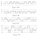
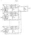
- Figure 1 is a schematic of the circuit and Figures 2A through 2D are diagrams of ternary input signals that could be used by the circuit in Figure 1.
- a ternary signal is defined as a signal with positive, zero, and negative polarities.
- a ternary signal differs from a trinary signal in that a trinary signal is limited to a single polarity, either positive or negative, even though it uses three levels of that polarity.
- the circuit disclosed herein will work with ternary signals having multiple levels of each polarity. Likewise, it will work also with signals having a single positive or negative polarity.
- the ternary signal depicted by Figure 2C will be used to describe the operation of the circuit.
- input lines 10, 20, n0 are connected to the input sides of input stages 100, 200, n00 respectively through transformers 102 202, ...n02 having a primary winding 136 236,...n36 and a secondary winding 138, 238,...n38.
- the output sides of input stages 100, 200, n00 are connected to a transformer 114 having a primary winding 140 and a secondary winding 142.
- the output of the input stages 100, 200, n00 are connected to a common output line 17 through transformer 114. Since each input stage 100, 200, n00 is identical to the other input stages 100, 200, n00, the circuit will be described in terms of input stage 100 with an understanding that the other input stages, 200, n00 operate in like fashion.
- isolation of input line 10 from the output of other input stages 200, n00 is accomplished as follows.
- a ternary signal on input line 10 will pass through input stage 100 to output line 17.
- Signals from other input stages will be prevented from feeding back into input line 10 by isolation circuitry comprised of transistor-diode combination 104 and 108, parallel oppositely poled transistor-diode combination 106 and 110 and resistor 112 in the input stage.
- the circuitry allows ternary signals to pass in one direction only, from input line 10 to output line 17.
- Signals from the output of other input stages 200, n00 will be prevented from feeding back into input line 10 due to a high impedance block that is created by the isolation circuitry 104-112 in response to signals from other input stages 200, n00 as will hereinafter be more fully explained.
- isolation of input line 10 is provided by transistor-diode combination 104 and 108 that comprises part of signal path 102, 104, 108, 114 and oppositely poled transistor-diode combination 106 and 110 that comprises part of signal path 102, 106, 110, 114 of input stage 100, and by resistor 112 which is used to bias transistors 104 and 106.
- the transistor-diode combination 104, 108 and transistor-diode combination 106, 110 allow signals originating on input line 10 to pass through one of the combinations 104 and 108 or 106 and 110.
- the transistor-diode combination 104, 108 or 106, 110 is selected by the polarity of the input signal.
- the transistor-diode combination 104, 108 and transistor-diode combination 106, 110 are connected in parallel and configured such that while an input signal of a given polarity on input line 10 will cause one transistor-diode combination to conduct and the other oppositely poled transistor-diode combination connected in parallel to reverse bias, a signal of any polarity produced by another input stage 200, n00 will reverse bias both transistor-diode combinations in input stage 100, thereby creating a high impedance block in the current path of output winding 138 of input transformer 102. By preventing current flow in the output winding 138 of input transformer 102 of input stage 100, the high impedance block will prevent signals from input stages 200, n00 from feeding back into input line 10. A detailed description of how the high impedance block is created by signals from other stages 200, n00 will be explained in the operation section.
- minimum attenuation is desirable because as attenuation is minimized, the possibility of error due to attenuated signal strength is reduced. Further, an attenuated signal may require amplification at some point, thereby increasing cost of operation and device complexity.
- the attenuation of the multiplexor disclosed herein is limited to the fixed drop of voltage across the components of the input stage. There is no progressive loss of signal energy as the number of input signal lines increase.
- minimization of attenuation is further enhanced by a step-up ratio in the input transformer 102 and a step-down ratio in the common output stage which is comprised of transformer 114. More specifically, the step-up/step-down ratios will reduce the relative amount of signal loss due to the saturation drop across the components 104-110 of input stage 100. Since these drops are relatively fixed by the circuit components, a large signal will have a proportionately smaller drop than a small signal.
- a typical turns ratio may be on the order of 4:1, but can vary due to specific values of circuit components, signal strength, etc. Therefore, the turns ratio selected is a matter of routine circuit design choice, as are the values for all of the other circuit components. A detailed description of how transformers 102, 114 operate to reduce signal attenuation is in the operation section.
- Each input stage 100, 200, n00 is completely passive, requiring no external power.
- the input signals power the circuit. Passive operation has several advantages. There is no requirement for a separate power supply, there is less complexity, there is more energy efficiency, and there is less expensive construction.
- Input stages are attached to output transformer 114 at 124 and 126 as shown in Figure 1. Signals passing through each of the plurality of input stages are processed in the same manner as the signal in input line 10, described above.
- Each input line 10, 20, n0 is connected to its own input stage 100, 200, n00, with its output connected in common to the output transformer 114. For ease of illustration, only 3 inputs 10, 20, n0 are shown in Figure 1. It is recognized that any number of input stages could be used depending on the number of input signals.
- the preferred embodiment uses lines which are balanced, both as to the inputs and the output.
- the alternative embodiments in Figures 3 and 4 are unbalanced lines which do not provide the output step-down transformer 114.
- a coax 134 and a resistor 132 are shown.
- Figure 3 shows an alternative embodiment of the invention.
- the output from each input stage 100, 200, n00 is connected directly to a coax cable 134.
- the circuit functions in the same manner as the circuit in Figure 1 with one exception. Due to the absence of the output step-down transformer, the ability to alter signal levels by stepping-up and then stepping down the signal to reduce attenuation as described in the preferred embodiment is not present.
- Figure 4 shows another embodiment of the invention.
- the output from each input stage 100, 200, n00 is connected to a resistive output 132.
- the ability to alter signal levels to reduce attenuation as described in the preferred embodiment is not present.
- Input line 10 is connected to input stage 100.
- a ternary signal appearing on input line 10 is separated into positive and negative pulses. The pulses will pass through input stage 100 by way of separate paths depending on the polarity of the pulse.
- a positive pulse will pass through input stage 100 using the path 102, 104, 108 and 114.
- a negative pulse will pass through input stage 100 using path 102, 106, 110, 114.
- Pulses produced by other input stages 200, n00, and appearing at the output of input stage 100 will be prevented from feeding back into input line 10 by a high impedance block created by the transistor-diode combination 104, 108, and transistor-diode combination 106, 110 in input stage 100.
- Ternary signals will pass from the input line 10 to the output line 17 as follows.
- a positive pulse on input line 10 will cause a positive pulse to appear between the output side 120 of input transformer 102 and the emitter of transistor 106, and a negative pulse to appear between the output side 122 of input transformer 102 and the collector of diode 110.
- the negative pulse from output side 122 of input transformer 102 will also be applied through resistor 112 to the base of transistor 106. Due to the positive pulse at the output 120 of input transformer 102 and the negative pulse at the base of transistor 106, transistor 106 will be reverse biased. Therefore, the transistor-diode combination 106, 110 will be prevented from passing the positive pulse on input line 10 through to output transformer 114.
- a positive pulse on input line 10 will cause a positive pulse to appear between the output side 120 of input transformer 102 and the emitter of transistor 104, and a negative pulse to appear between the output side 122 of input transformer 102 and the emitter of diode 108, the negative pulse will also be applied through resistor 112 to the base of transistor 104. Due to the positive pulse at the output 120 of input transformer 102 and the negative pulse at the base of transistor 104, transistor 104 will be forward biased, thus allowing the pulse to pass through to diode 108. Diode 108 will be forward biased due to the positive pulse applied to its collector by transistor 104 and the negative pulse applied to its emitter by the output side 122 of input transformer 102. Therefore, the transistor-diode combination 104, 108 will be forward biased causing current to flow through the path 102, 114, 108, 104. The current flow through transformer 114 will cause the positive pulse to appear on output line 17.
- a negative pulse on input line 10 will cause a negative pulse to appear between the output side 120 of input transformer 102 and the emitter of transistor 104, and a positive pulse to appear between the output side 122 of input transformer 102 and the emitter of diode 108.
- the positive pulse from output side 122 of input transformer 102 will also be applied through resistor 112 to the base of transistor 104. Due to the negative pulse at the output 120 of input transformer 102 and the positive pulse at the base of transistor 104, the transistor 104 will be reverse biased. Therefore, the transistor-diode combination 104, 108 will be prevented from passing the negative pulse on input line 10 through to output transformer 114.
- a negative pulse on input line 10 will cause a negative pulse to appear between the output side 120 of input transformer 102 and the emitter of transistor 106, and a positive pulse to appear between the output side 122 of input transformer 102 and the collector of diode 110.
- the positive pulse from output side 122 of input transformer 102 will also be applied through resistor 112 to the base of transistor 106. Due to the negative pulse at the output 120 of input transformer 102 and the positive pulse at the base of transistor 106, the transistor 106 will be forward biased, thus allowing the pulse to pass through to diode 110. Diode 110 will be forward biased due to the negative pulse applied to its emitter by transistor 106 and the positive pulse applied to its collector by the output side 122 of input transformer 102. Therefore, the transistor-diode combination 106, 110 will be forward biased causing current to flow through the path 102, 114, 110, 106. The current flow through transformer 114 will cause the negative pulse to appear on output line 17.
- Isolation of input stage 100 is achieved as follows.
- a positive pulse from another input stage 200, n00 will produce a positive pulse on the input side 124 of output transformer 114 and a negative pulse on the input side 126 of output transformer 114.
- the positive pulse on the input side 124 of output transformer 114 will apply to the emitter of diode 108.
- Diode 108 will be reverse biased by the positive pulse, thereby preventing conduction through transistor-diode combination 104, 108.
- the negative pulse on the input side 126 of output transformer 114 will apply a negative pulse through resistor 112 to the base of transistor 106.
- Transistor 106 will be reverse biased by the negative pulse, thereby preventing conduction through transistor-diode combination 106, 110.
- a negative pulse from another input stage 200, n00 will produce a negative pulse on the input side 124 of output transformer 114 and a positive pulse on the input side 126 of output transformer 114.
- the negative pulse on the input side 124 of output transformer 114 will apply to the collector of diode 110.
- Diode 110 will be reverse biased by the negative pulse, thereby preventing conduction through transistor-diode combination 106, 110.
- the positive pulse on the input side 126 of output transformer 114 will apply a positive pulse through resistor 112 to the base of transistor 104.
- Transistor 104 will be reverse biased by the positive pulse, thereby preventing conduction through transistor-diode combination 104, 108.
- the input and output transformers 102, 114 are reciprocal in turns ratio and impedance ratio so that the transformers 102, 114 are substantially transparent to the line.
- the input transformer 102 has a step-up ratio to increase the voltage level of the input signal and output transformer 114 has a step-down ratio to restore the signal voltage to level existing on input line 10.
- the higher level signal that results from the step-up ratio will produce the same voltage drop across the components 104-112 of input stage 100 as the signal would at its original level prior to being stepped-up by input transformer 102.
- the output transformer 114 has a step-down ratio equal to the step-up ratio of input transformer 102.
- the result of temporarily stepping up the signal while it passes through the multiplexor is to reduce the amount of signal loss due to attenuation.
- the following example can be used to illustrate the effect of the step-up/step-down ratios on signal attenuation. The values used for signal levels were chosen for ease of illustration.
- input transformer 102 has a 1:1 ratio (no step-up)
- output transformer 114 also has a 1:1 ratio (no step-down)
- the components 104-112 of input stage 100 create a 1 volt drop in signal level.
- a 4 volt signal applied to the input winding 136 of input transformer 102 would produce a 4 volt signal at the output winding 138 of input transformer 102.
- a signal drop of 1 volt due to the characteristics of the components 104-112 of input stage 100 would result in the application of a signal level of 3 volts to the input winding 140 of output transformer 114. Therefore, the signal at the output winding 142 of output transformer 114 would be 3 volts.
- the output signal level would be as follows.
- An input signal of 4 volts applied to the input winding 136 of input transformer 102 would produce a 16 volt signal at the output winding 138 of input transformer 102.
- a loss of 1 volt in signal level due to voltage drop across the components 104-112 of input stage 100 would result in application of a 15 volt signal level to the input winding 140 of output transformer 114.
- the 4:1 step-down ratio of output transformer 114 would result in a signal level of 3.75 volts at the output winding 142 of output transformer 114, thereby significantly reducing the effects of attenuation due to circuit components.
- Input stage 100 is completely passive, requiring no external power supply. The power required to pass the input signal on input line 10 through input stage 100 to output transformer 114 is provided solely by the input signal on line 10.
- the circuit multiplexes the plurality of input ternary signals while simultaneously achieving a high level of isolation of input lines, minimizing attenuation of the signal, eliminating the need for an external power supply through passive operation, and reducing fabrication costs by being constructed with a small number of components.
Landscapes
- Engineering & Computer Science (AREA)
- Power Engineering (AREA)
- Electronic Switches (AREA)
- Time-Division Multiplex Systems (AREA)
- Dc Digital Transmission (AREA)
- Logic Circuits (AREA)
Applications Claiming Priority (2)
| Application Number | Priority Date | Filing Date | Title |
|---|---|---|---|
| US07/100,061 US4814634A (en) | 1987-09-23 | 1987-09-23 | Ternary signal multiplexor circuit |
| US100061 | 1987-09-23 |
Publications (2)
| Publication Number | Publication Date |
|---|---|
| EP0308632A2 true EP0308632A2 (fr) | 1989-03-29 |
| EP0308632A3 EP0308632A3 (fr) | 1990-07-18 |
Family
ID=22277924
Family Applications (1)
| Application Number | Title | Priority Date | Filing Date |
|---|---|---|---|
| EP88112551A Withdrawn EP0308632A3 (fr) | 1987-09-23 | 1988-08-02 | Circuit multiplex pour signaux ternaires |
Country Status (3)
| Country | Link |
|---|---|
| US (1) | US4814634A (fr) |
| EP (1) | EP0308632A3 (fr) |
| JP (1) | JPS6490629A (fr) |
Families Citing this family (3)
| Publication number | Priority date | Publication date | Assignee | Title |
|---|---|---|---|---|
| US5390181A (en) * | 1993-06-04 | 1995-02-14 | Illinois Institute Of Technology | Method for detecting collisions on and controlling access to a transmission channel |
| DE10039248C2 (de) * | 2000-08-11 | 2002-10-24 | Zeiss Carl Jena Gmbh | Verfahren zur elektronischen Bildentzerrung bei Laser-Scan-Einrichtungen |
| US7825745B1 (en) * | 2006-09-12 | 2010-11-02 | Rf Magic Inc. | Variable bandwidth tunable silicon duplexer |
Family Cites Families (13)
| Publication number | Priority date | Publication date | Assignee | Title |
|---|---|---|---|---|
| US2889537A (en) * | 1955-10-28 | 1959-06-02 | Gen Dynamics Corp | Electronic selector switch |
| US3453495A (en) * | 1965-10-24 | 1969-07-01 | Cons Edison Co | Reverse current flow protector for electric power systems |
| US3832494A (en) * | 1970-06-10 | 1974-08-27 | Control Data Corp | Signal multiplexer and demultiplexer |
| US3842401A (en) * | 1973-09-10 | 1974-10-15 | Gen Electric | Ternary code error detector for a time-division multiplex, pulse-code modulation system |
| US3904977A (en) * | 1973-10-05 | 1975-09-09 | Ibm | Multiplexing switch with wide bandpass characteristics and high isolation impedance between inputs |
| US4087642A (en) * | 1974-05-07 | 1978-05-02 | International Standard Electric Corporation | Digital data communication system |
| US3974397A (en) * | 1975-04-01 | 1976-08-10 | S & C Electric Company | Multi-phase rectifier system |
| FR2333392A1 (fr) * | 1975-11-25 | 1977-06-24 | Europ Teletransmission | Multiplexeur et demultiplexeur pour multiplexage a impulsions codees |
| US4010385A (en) * | 1976-01-09 | 1977-03-01 | Teletype Corporation | Multiplexing circuitry for time sharing a common conductor |
| DK143627C (da) * | 1978-10-30 | 1982-02-15 | Rovsing A S | Koblingskreds til overfoering af datasignaler med stor hastighed |
| US4243976A (en) * | 1979-03-12 | 1981-01-06 | The Singer Company | Ternary to binary converter |
| US4387460A (en) * | 1979-07-23 | 1983-06-07 | Societe Anonyme De Tele-Communication | Supplementary information transmitting arrangement for a digital data transmission system |
| US4649548A (en) * | 1981-03-11 | 1987-03-10 | Crane Ronald C | Local computer network transceiver |
-
1987
- 1987-09-23 US US07/100,061 patent/US4814634A/en not_active Expired - Fee Related
-
1988
- 1988-08-02 EP EP88112551A patent/EP0308632A3/fr not_active Withdrawn
- 1988-08-12 JP JP63200309A patent/JPS6490629A/ja active Granted
Also Published As
| Publication number | Publication date |
|---|---|
| EP0308632A3 (fr) | 1990-07-18 |
| JPH043141B2 (fr) | 1992-01-22 |
| US4814634A (en) | 1989-03-21 |
| JPS6490629A (en) | 1989-04-07 |
Similar Documents
| Publication | Publication Date | Title |
|---|---|---|
| DE3851970T2 (de) | Übertragungssystem für Binärdaten. | |
| DE1512073B2 (de) | Teilnehmerschaltung fuer eine fernsprechanlage | |
| US3970784A (en) | Transmission system | |
| US3610963A (en) | Switch drive circuit for the time ratio controlled transistor switching circuits | |
| US4814634A (en) | Ternary signal multiplexor circuit | |
| EP0260752A1 (fr) | Circuit hybride actif à équilibrage symétrique | |
| US3424858A (en) | Line communications system including an electric amplifier composed of similar transistors | |
| GB1407246A (en) | High voltage switching systems | |
| DE2613929C3 (de) | Schaltungsanordnung mit einem Relais, das einen Arbeitskontakt aufweist | |
| DE2927607C2 (de) | Schaltungsanordnung zum Zuführen eines Signals zu einer Übertragungsleitung | |
| US3943432A (en) | Electronic feeding bridge | |
| US5093587A (en) | ECL bidirectional bus for use in a network with modules which employs high resistance interconnect technology between module | |
| US4639620A (en) | Parallel-series converter | |
| US3176152A (en) | Current switching transistor system utilizing tunnel diode coupling | |
| DE2925747C2 (de) | Schaltungsanordnung für einen elektronischen Gleichstrom-Telegrafiesender | |
| US4172215A (en) | Transformer coupling circuit providing for cancellation of D.C. fluxes | |
| US5448076A (en) | Optically-coupled differential line driver generating an optical signal having at least three states | |
| US4234763A (en) | Feeding bridge with d.c.-compensation for both directions of the feed current | |
| US5332894A (en) | Optical output control IC and optical input amplifier IC | |
| US4373118A (en) | Battery feed circuit | |
| DE3407226C2 (fr) | ||
| GB1386339A (en) | Combiner network | |
| EP0048490A1 (fr) | Circuit pour transformer un signal d'entrée binaire en un signal télégraphique | |
| US3047842A (en) | Magnetic-core shift register | |
| DE1562261B1 (de) | Schaltmatrix fuer eine selbsttaetige Schaltvorrichtung z.B. eine Selbstwaehlfernsprechanlage |
Legal Events
| Date | Code | Title | Description |
|---|---|---|---|
| PUAI | Public reference made under article 153(3) epc to a published international application that has entered the european phase |
Free format text: ORIGINAL CODE: 0009012 |
|
| AK | Designated contracting states |
Kind code of ref document: A2 Designated state(s): DE FR GB |
|
| 17P | Request for examination filed |
Effective date: 19890720 |
|
| PUAL | Search report despatched |
Free format text: ORIGINAL CODE: 0009013 |
|
| AK | Designated contracting states |
Kind code of ref document: A3 Designated state(s): DE FR GB |
|
| 17Q | First examination report despatched |
Effective date: 19920103 |
|
| STAA | Information on the status of an ep patent application or granted ep patent |
Free format text: STATUS: THE APPLICATION IS DEEMED TO BE WITHDRAWN |
|
| 18D | Application deemed to be withdrawn |
Effective date: 19940301 |