EP0308959B1 - Empfänger, geeignet für die Verbesserung des Geräuschabstands bei der Wiedergabe digitaler Signale - Google Patents
Empfänger, geeignet für die Verbesserung des Geräuschabstands bei der Wiedergabe digitaler Signale Download PDFInfo
- Publication number
- EP0308959B1 EP0308959B1 EP88115695A EP88115695A EP0308959B1 EP 0308959 B1 EP0308959 B1 EP 0308959B1 EP 88115695 A EP88115695 A EP 88115695A EP 88115695 A EP88115695 A EP 88115695A EP 0308959 B1 EP0308959 B1 EP 0308959B1
- Authority
- EP
- European Patent Office
- Prior art keywords
- digital signal
- signal
- tap gains
- binary
- noise
- Prior art date
- Legal status (The legal status is an assumption and is not a legal conclusion. Google has not performed a legal analysis and makes no representation as to the accuracy of the status listed.)
- Expired - Lifetime
Links
- 230000004044 response Effects 0.000 claims description 15
- 230000005540 biological transmission Effects 0.000 claims description 10
- 238000001228 spectrum Methods 0.000 claims description 5
- 238000001914 filtration Methods 0.000 claims description 4
- 230000003111 delayed effect Effects 0.000 description 4
- 238000010586 diagram Methods 0.000 description 4
- 230000003044 adaptive effect Effects 0.000 description 2
- 230000006978 adaptation Effects 0.000 description 1
- 230000006870 function Effects 0.000 description 1
Images

Classifications
-
- H—ELECTRICITY
- H04—ELECTRIC COMMUNICATION TECHNIQUE
- H04L—TRANSMISSION OF DIGITAL INFORMATION, e.g. TELEGRAPHIC COMMUNICATION
- H04L25/00—Baseband systems
- H04L25/02—Details ; arrangements for supplying electrical power along data transmission lines
- H04L25/03—Shaping networks in transmitter or receiver, e.g. adaptive shaping networks
- H04L25/03006—Arrangements for removing intersymbol interference
- H04L25/03012—Arrangements for removing intersymbol interference operating in the time domain
- H04L25/03019—Arrangements for removing intersymbol interference operating in the time domain adaptive, i.e. capable of adjustment during data reception
- H04L25/03057—Arrangements for removing intersymbol interference operating in the time domain adaptive, i.e. capable of adjustment during data reception with a recursive structure
Definitions
- This invention relates to a receiver for receiving a digital signal transmitted through a transmission path to reproduce the transmitted digital signal as a reproduced digital signal.
- a receiver of the type described is supplied with a transmitted digital signal which is transmitted through a transmission path of a first frequency characteristic and which is inevitably subjected to noise. It is therefore necessary in the receiver not only to equalize the transmitted digital signal but also to remove the noise.
- the receiver comprises a feedback digital filter for equalizing the transmitted digital signal.
- a proposal is made about reduction of the noise by using a matched filter which has an infinite delay time. However, it is practically difficult to implement such a matched filter having the infinite delaying time.
- the improved receiver comprises a linear filter and the feedback digital filter.
- the linear filter is used as a filter section and has a second frequency characteristic.
- the feedback digital filter is used as an equalizer section.
- the linear filter filters the transmitted digital signal into a filtered digital signal.
- the feedback decision equalizer equalizes the filtered digital signal into an equalized digital signal in response to controllable tap gains.
- the controllable tap gains are controlled by a tap gain controller in accordance with the first and second frequency characteristics to make the linear filter produce the equalized digital signal as the reproduced digital signal.
- the linear filter can not sufficiently get rid of the noise introduced into the transmitted digital signal.
- the filtered digital signal is accompanied with a noise signal and is applied to the feedback digital filter together with the noise signal.
- the equalized digital signal is produced with the noise from the feedback decision equalizer. This makes it difficult to achieve a satisfactory signal-to-noise ratio in the reproduced digital signal.
- Said receiver comprises a filter section with a filter and an A/D converter for filtering said transmitted digital signal into a filtered digital signal, a decision feedback equalizer for equalizing said filtered digital signal into an equalized digital signal in response to controllable tap gains, and a tap gain adaptation for controlling said controllable tap gains to make said equalizer section produce said equalized digital signal as said reproduced digital signal.
- Said equalizer section comprises a forward filter for filtering said filtered digital signal in response to predetermined ones of said controllable tap gains; and a backward filter for equalizing in response to remaining ones of said controllable tap gains to produce said reproduced digital signal.
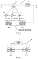
- a receiver has receiver input and output terminals 11 and 12.
- a transmission path 13 which may be a radio channel, a transmitted digital signal is supplied to the receiver input terminal 11 as a received digital signal.
- the transmitted digital signal may be, for example, a binary signal.
- the transmitted digital signal is carried by a carrier signal of a carrier angular frequency ⁇ and is transmitted at a predetermined transmission rate R.
- the transmission path 13 has a first frequency characteristic T( ⁇ ).
- the received digital signal is inevitably accompanied by noise to which the transmitted digital signal is subjected while being transmitted through the transmission path 13.
- the receiver comprises a filter section 16 connected to the receiver input terminal 11.
- the filter section 16 filters the received digital signal into a filtered digital signal in accordance with a second frequency characteristic H( ⁇ ). Due to the noise accompanying the received digital signal, the filtered digital signal is accompanied by a noise signal.
- An equalizer section 17 is given a plurality of controllable tap gains in the manner which is known in the art and will become clear as the description proceeds.
- the equalizer section 17 equalizes the filtered digital signal into an equalized digital signal in response to the controllable tap gains and delivers the equalized digital signal to the receiver output terminal 12 as a reproduced digital signal which is a reproduction of the transmitted digital signal exempted substantially from the noise.
- the equalizer section 17 includes a tap gain controller 18 which keeps the first and the second frequency characteristics.
- the controllable tap gains are controlled by the tap gain controller 18 in accordance with the first and the second frequency characteristics. According to this invention, the controllable tap gains are classified into predetermined tap gains and remaining tap gains.
- the equalizer section 17 comprises a transversal filter 21 and a decision equalizer 22.
- the filtered digital signal is supplied to the transversal filter 21 from the filter section 16.
- the transversal filter 21 filters the filtered digital signal into an intermediate digital signal in response to the predetermined tap gains. In this manner, the transversal filter 21 is operable as a first arrangement.
- the decision equalizer 22 is supplied with the intermediate digital signal and equalizes the intermediate digital signal into the equalized digital signal in response to the remaining tap gains.
- the equalized digital signal is delivered to the receiver output terminal 12 as the reproduced digital signal.
- the decision equalizer 22 is operable as a second arrangement.
- the transversal filter 21 has filter input and output terminals 31 and 32.
- the filtered digital signal is supplied to the filter input terminal 31.
- the transversal filter 21 comprises a filter shifting memory circuit 33 having first through M-th filter registers 34-1, 34-2, ..., and 34-M connected in cascade, where M may be, for example, six.
- the filter shifting memory circuit 33 has first through M-th transversal filter taps 35-1, 35-2, ..., 35-(M-1), and 35-M corresponding to the filter registers 34-1 to 34-M, respectively.
- the input terminal 31 corresponds to a zeroth tap.
- Transversal filter taps 35-1 to 35-M are connected to first through M-th filter multipliers 36-1, 36-2, ..., 36-(M-1), and 36-M.
- the tap gain controller 18 (Fig. 1) supplies first through M-th predetermined tap gains d1 to d M to the first through the M-th filter multipliers 36-1 to 36-M.
- the filter multipliers 36-1 to 36-M are connected to a filter adder 37.
- the filter adder 37 is connected to the decision equalizer 22 (Fig. 1) through the filter output terminal 32.
- the filtered digital signal is supplied to the first register 34-1 and the adder 37 through the filter input terminal 31.
- Each of the first through the M-th filter registers gives a delay of 1/R to a signal supplied thereto.
- the first through the M-th registers 34-1 to 34-M supply first through M-th delayed digital signals to the first through the M-th multipliers 36-1 to 36-M through the first through the M-th transversal filter taps 35-1 to 35-M, respectively.
- the first multiplier 36-1 multiplies the first delayed digital signal by the first predetermined tap gain d1.
- the first through the M-th multipliers 36-1 to 36-M deliver first through M-th multiplied digital signals, respectively, to the adder 37.
- the adder 37 calculates a total sum of the filtered digital signal and the first through the M-th multiplied digital signals to produce a sum digital signal as the intermediate digital signal.
- the sum digital signal is delivered to the decision equalizer 17 through the filter output terminal 22.
- the sum digital signal is produced in the form of a binary signal.
- the decision equalizer 22 has equalizer input and output terminals 41 and 42.
- the sum digital signal is supplied to the equalizer input terminal 41 from the transversal filter 21 (Fig. 1).
- the decision equalizer 22 comprises a decision equalizer adder 43 and a judging circuit 44 connected to the decision equalizer adder 43.
- the judging circuit 44 is connected to a decision equalizer shifting memory circuit 45 having first through N-th decision equalizer registers 46-1, 46-2, ..., and 46-N connected in cascade, where N may be, for example, fifteen.
- the decision equalizer shifting memory circuit 45 has first through N-th decision equalizer taps 47-1, 47-2, ..., and 47-N corresponding to the decision equalizer registers 46-1 to 46-N, respectively.
- Each of decision equalizer taps 47-1 to 47-N is connected to first through N-th decision equalizer multipliers 48-1, 48-2, ..., and 48-N.
- the tap gain controller 18 (Fig. 1) supplies first through N-th remaining tap gains c1 to c N to the first through the N-th decision equalizer multipliers 48-1 to 48-N.
- the decision equalizer multipliers 48-1 to 48-N are connected to the decision equalizer adder 43.
- the sum digital signal is supplied to the judging circuit 44 through the decision equalizer adder 43.
- the judging circuit 44 has a predetermined threshold level.
- the judging circuit 44 judges at first the sum digital signal whether or not the sum digital signal has a binary level above the predetermined threshold level to decide a judged binary level for the binary level.
- the judging circuit 44 thereby produces a judged digital signal having the judged binary level.
- the judging circuit 44 delivers the judged digital signal to the first decision equalizer register 46-1.
- the first through the N-th decision equalizer registers 46-1 to 46-N supply first through the N-th decision equalizer delayed digital signal to the first through the N-th decision equalizer multipliers 48-1 to 48-N through the first through the N-th decision equalizer taps 47-1 to 47-N, respectively.
- Each of the decision equalizer registers 46-1 to 46-N gives a delay of 1/R to an input signal supplied thereto.
- the first decision equalizer multiplier 48-1 multiplies the first decision equalizer delayed digital signal by the first remaining tap gain c1.
- the first through the N-th decision equalizer multipliers 48-1 to 48-N deliver first through N-th decision equalizer multiplied digital signals, respectively, to the decision equalizer adder 43.
- the decision equalizer adder 43 subtracts a sum of the first through the N-th decision equalizer multiplied digital signals from the sum digital signal to produce a subtracted digital signal.
- the subtracted digital signal is produced in the form of a binary signal.
- the subtracted digital signal is supplied to the judging circuit 44 and is judged by the judging circuit 44 to be produced as the reproduced digital signal.
- the reproduced digital signal is delivered from the equalizer output terminal 42 to the receiver output terminal 12.
- the tap gain controller 18 comprises a memory part 51, a first determining part 52, and a second determining part 53.
- the memory part 51 memorizes the first and the second frequency characteristics and a noise spectrum N( ⁇ ) of the noise signal accompanying the filtered digital signal.
- the first determining part 52 determines the first through the M-th predetermined tap gains d1 to d M in response to the second frequency characteristic H( ⁇ ) and the noise spectrum N( ⁇ ).
- the first determining part 52 supplies the first through the M-th predetermined tap gains d1 to d M to the first and the M-th filter multipliers 36-1 to 36-M and to the second determining part 53.
- the second determining part 53 determines the first through the N-th remaining tap gains c1 to c N in response to the first and the second frequency characteristics T( ⁇ ) and H( ⁇ ) and the first through the M-th predetermined tap gains d1 to d M supplied from the first determining part 52.
- the second determining part 53 supplies the first through the N-th remaining tap gains c1 to c N to the first through the N-th decision equalizer multipliers 48-1 to 48-N, respectively.
- the transversal filter 21 has a third frequency characteristic G( ⁇ ) given as follows: where d(i) represents the first through the M-th predetermined tap gains d1 to d M and a zeroth tap gain d0 which is equal to unity and where t(i) represents zeroth through M-th time instants having a time duration of 1/R between two consecutive ones of the time instants.
- the zeroth time instant t0 represents a time instant at which the filtered digital signal is supplied to the transversal filter 21.
- the transversal filter 21 produces the intermediate digital signal which may be accompanied by a small noise signal of a noise power ⁇ 2.
- the noise power is given by:
- Equation (3) the noise power is represented as a quadratic having a positive coefficient related to the zeroth through the M-th predetermined tap gains d0 to d M .
- the first determining part 52 determines the first through the M-th predetermined tap gains d1 to d M by minimizing the noise power.
- a microprocessor may be used as the first determining part 52. Responsive to the first through the M-th predetermined tap gains d1 to d M supplied to the first through the M-th filter multipliers 35-1 to 35-M, the transversal filter 21 filters the filtered digital signal into the intermediate digital signal so as to minimize the noise power of the intermediate digital signal.
- the second determining part 53 calculates the first through the N-th levels g1 to g N according to Equation (4).
- a microprocessor may be used as the second determining part 53.
- the second determining part 53 thereby supplies the decision equalizer 22 with the first through the N-th levels g1 to g N as the first through the N-th remaining tap gains c1 to c N , respectively.
- the decision equalizer 22 equalizes the intermediate digital signal into the equalized digital signal.
Landscapes
- Engineering & Computer Science (AREA)
- Power Engineering (AREA)
- Computer Networks & Wireless Communication (AREA)
- Signal Processing (AREA)
- Cable Transmission Systems, Equalization Of Radio And Reduction Of Echo (AREA)
- Filters That Use Time-Delay Elements (AREA)
- Noise Elimination (AREA)
- Circuits Of Receivers In General (AREA)
Claims (3)
- Empfänger für den Empfang eines auf einem Übertragungspfad mit einer ersten Frequenzcharakteristik übertragenen Digitalsignals, um jenes übertragene Digitalsignal als Wiedergabe-Digitalsignal wiederzugeben, wobei der Empfänger aufweist: ein Filterteil (16), das eine zweite Frequenzcharakteristik zur Filterung jenes übertragenen Digitalsignals in ein von einem Rauschsignal begleitetes, gefiltertes Digitalsignal besitzt, ein Entzerrerteil (17) zum Entzerren des gefilterten Digitalsignals in ein entzerrtes Digitalsignal als Antwort auf steuerbare Stufenverstärkungen und eine Steuereinrichtung (18) zum Steuern der steuerbaren Stufenverstärkungen in Übereinstimmung mit den ersten und zweiten Frequenzcharakteristika, um das Entzerrerteil zu veranlassen, das entzerrte Digitalsignal als das Wiedgergabe-Digitalsignal zu erzeugen, wobei das Entzerrerteil (17) umfaßt:
eine erste Einrichtung (21) zum Filtern des gefilterten Digitalsignals als Antwort auf die vorgegebenen der steuerbaren Stufenverstärkungen, um ein Zwischendigitalsignal zu erzeugen, und
eine zweite Einrichtung (22) zum Entzerren des Zwischendigitalsignals in das entzerrte Digitalsignal als Antwort auf die verbleibenden der steuerbaren Stufenverstärkungen, um das Wiedergabe-Digitalsignal zu erzeugen, dadurch gekennzeichnet, daß
die Steuereinrichtung (18) eine Einrichtung (52) zum Steuern der vorgegebenen Stufenverstärkungen, um die Rauschleistung des Rauschsignals in dem Zwischendigitalsignal zu minimieren, und eine Einrichtung (53) zum Steuern der verbleibenden Stufenverstärkungen aufweist, um das Zwischendigitalsignal in das Wiedergabe-Digitalsignal zu entzerren. - Empfänger nach Anspruch 1, wobei die Steuereinrichtung (18) eine Speichereinrichtung (51) zum Speichern der ersten und zweiten Frequenzcharakteristika und eines Rauschspektrums des Rauschsignals aufweist, wobei die erste Steuereinrichtung (52) auf die zweite Frequenzcharakteristik und auf das Rauschspektrum anspricht, um die vorgegebenen Stufenverstärkugen zu bestimmen, und wobei die zweite Steuereinrichtung (53) auf die erste und die zweite Frequenzcharakteristika und die vorgegebenen Stufenverstärkungen anspricht, um die verbleibenden Schaltverstärkungsgrade zu bestimmen.
- Empfänger nach Anspruch 1 oder 2, wobei das Zwischendigitalsignal ein Zwischenbinärsignal ist, die zweite Einrichtung eine Beurteilungsschaltung (44) zur Beurteilung, ob ein Eingangsbinärsignal einen Binärpegel über einem vorgegebenen Schwellpegel besitzt, aufweist, um einen beurteilten Binärpegel für den Eingangsbinärpegel zu bestimmen, die Beurteilungsschaltung dabei ein Ausgangsbinärsignal mit dem beurteilten Binärpegel erzeugt, und die zweite Einrichtung ferner Modifizierungseinrichtungen (43, 45, 47, 48) zum Modifizieren einer Kombination des Zwischenbinärsignals und des Ausgangsbinärsignals zu einem modifizierten Binärsignal als Antwort auf die verbleibenden Stufenverstärkungen und eine Einrichtung (43) zur Belieferung der Beurteilungsschaltung zuerst mit dem Zwischenbinärsignal als dem Eingangsbinärsignal und darauffolgend mit dem modifizierten Binärsignal aufweist, wobei die Beurteilungsschaltung das Ausgangsbinärsignal als das entzerrte Digitalsignal erzeugt, wenn sie mit dem modifizierten Binärsignal beliefert wird.
Applications Claiming Priority (2)
| Application Number | Priority Date | Filing Date | Title |
|---|---|---|---|
| JP62238990A JPH0750863B2 (ja) | 1987-09-25 | 1987-09-25 | 受信器 |
| JP238990/87 | 1987-09-25 |
Publications (3)
| Publication Number | Publication Date |
|---|---|
| EP0308959A2 EP0308959A2 (de) | 1989-03-29 |
| EP0308959A3 EP0308959A3 (en) | 1990-10-31 |
| EP0308959B1 true EP0308959B1 (de) | 1994-12-14 |
Family
ID=17038279
Family Applications (1)
| Application Number | Title | Priority Date | Filing Date |
|---|---|---|---|
| EP88115695A Expired - Lifetime EP0308959B1 (de) | 1987-09-25 | 1988-09-23 | Empfänger, geeignet für die Verbesserung des Geräuschabstands bei der Wiedergabe digitaler Signale |
Country Status (6)
| Country | Link |
|---|---|
| US (1) | US4972433A (de) |
| EP (1) | EP0308959B1 (de) |
| JP (1) | JPH0750863B2 (de) |
| AU (1) | AU611948B2 (de) |
| CA (1) | CA1312356C (de) |
| DE (1) | DE3852454T2 (de) |
Families Citing this family (14)
| Publication number | Priority date | Publication date | Assignee | Title |
|---|---|---|---|---|
| US4995106A (en) * | 1989-08-24 | 1991-02-19 | Ampex Corporation | Fast decision feedback decoder for digital data |
| ES2208713T3 (es) * | 1989-10-17 | 2004-06-16 | Paragon Ag | Dispositivo sensor de gas. |
| US5111481A (en) * | 1989-11-17 | 1992-05-05 | Nynex Corporation | Dual mode LMS channel equalizer |
| JP2543215B2 (ja) * | 1990-03-19 | 1996-10-16 | 松下電器産業株式会社 | デ―タ受信装置 |
| US5481564A (en) * | 1990-07-20 | 1996-01-02 | Fujitsu Limited | Received data adjusting device |
| JP3251023B2 (ja) * | 1991-02-27 | 2002-01-28 | 日本電気株式会社 | 自動等化器 |
| US5327460A (en) * | 1992-07-07 | 1994-07-05 | National Semiconductor Corporation | Method and apparatus for filtering post decision feedback equalization noise |
| US5408696A (en) * | 1992-12-11 | 1995-04-18 | Telefonaktiebolaget L M Ericsson | Method and apparatus for correcting a radio signal strength information signal |
| JPH0738560B2 (ja) * | 1993-02-23 | 1995-04-26 | 日本電気株式会社 | 自動等化器 |
| US5572552A (en) * | 1994-01-27 | 1996-11-05 | Ericsson Ge Mobile Communications Inc. | Method and system for demodulation of downlink CDMA signals |
| FR2732178A1 (fr) * | 1995-03-22 | 1996-09-27 | Philips Electronique Lab | Systeme de transmission numerique muni d'un recepteur a egaliseurs cascades |
| US6166594A (en) * | 1999-09-01 | 2000-12-26 | Zenith Electronics Corporation | Self calibrating demodulator system |
| JP2005159466A (ja) * | 2003-11-20 | 2005-06-16 | Sanyo Electric Co Ltd | 等化方法およびそれを利用した受信装置 |
| US7483479B2 (en) * | 2004-09-16 | 2009-01-27 | Keyeye Communications | Scaled signal processing elements for reduced filter tap noise |
Family Cites Families (8)
| Publication number | Priority date | Publication date | Assignee | Title |
|---|---|---|---|---|
| US3708766A (en) * | 1970-12-31 | 1973-01-02 | Ibm | Automatic equalizer and method of operation therefor |
| US3795865A (en) * | 1972-02-23 | 1974-03-05 | Honeywell Inf Systems | Automated real time equalized modem |
| FR2482809B1 (fr) * | 1980-05-14 | 1986-11-14 | Labo Electronique Physique | Systeme adaptatif de reception de donnees numeriques a compensation des distorsions d'amplitude et de phase introduites par le canal de transmission des donnees |
| US4359778A (en) * | 1981-02-05 | 1982-11-16 | Zenith Radio Corporation | Channel equalizer and method for cancelling ghosts |
| JPS592448A (ja) * | 1982-06-28 | 1984-01-09 | Fujitsu Ltd | 自動等化器発散検出方式 |
| IT1188626B (it) * | 1986-03-25 | 1988-01-20 | Gte Telecom Spa | Metodo e dispositivo di equalizzazione adattiva cieca |
| US5042026A (en) * | 1987-03-03 | 1991-08-20 | Nec Corporation | Circuit for cancelling whole or part of a waveform using nonrecursive and recursive filters |
| EP0300449B1 (de) * | 1987-07-21 | 1994-06-08 | Nec Corporation | Digitaler automatischer Leitungsentzerrer mit Mitteln zur Regelung der Anzapfungsverstärkung in Abhängigkeit der mittleren Filterausgangsleistung |
-
1987
- 1987-09-25 JP JP62238990A patent/JPH0750863B2/ja not_active Expired - Lifetime
-
1988
- 1988-09-22 CA CA000578089A patent/CA1312356C/en not_active Expired - Fee Related
- 1988-09-23 AU AU22766/88A patent/AU611948B2/en not_active Ceased
- 1988-09-23 EP EP88115695A patent/EP0308959B1/de not_active Expired - Lifetime
- 1988-09-23 DE DE3852454T patent/DE3852454T2/de not_active Expired - Fee Related
- 1988-09-26 US US07/249,068 patent/US4972433A/en not_active Expired - Fee Related
Also Published As
| Publication number | Publication date |
|---|---|
| DE3852454T2 (de) | 1995-05-04 |
| EP0308959A2 (de) | 1989-03-29 |
| EP0308959A3 (en) | 1990-10-31 |
| DE3852454D1 (de) | 1995-01-26 |
| AU611948B2 (en) | 1991-06-27 |
| JPH0750863B2 (ja) | 1995-05-31 |
| JPS6482824A (en) | 1989-03-28 |
| US4972433A (en) | 1990-11-20 |
| CA1312356C (en) | 1993-01-05 |
| AU2276688A (en) | 1989-04-06 |
Similar Documents
| Publication | Publication Date | Title |
|---|---|---|
| US5432522A (en) | Cross polarization interference compensating device comprising decision feedback cross polarization interference cancellers | |
| US5394110A (en) | Demodulation system having adaptive matched filter and decision feedback equalizer | |
| EP0755141B1 (de) | Adaptive, entscheidungsrückgekoppelte Entzerrung für Kommunikationssysteme | |
| US4972433A (en) | Receiver capable of improving signal-to-noise ratio in reproducing digital signal | |
| CA1276246C (en) | Digital automatic line equalizer for communication system | |
| US5661528A (en) | Apparatus and method for controlling operation of a high defination television adaptive equalizer | |
| US5359628A (en) | Channel impulse response estimator for use in an adaptive maximum likelihood sequence estimation receiver which is applicable to a communication system having a channel characteristic with rapid fluctuation | |
| EP0532353B1 (de) | Schneller entscheidungsrückgekoppelter Entzerrer mit niedrigem Restschwund | |
| US5327458A (en) | Automatic equalizer capable of effectively cancelling intersymbol interference and cross polarization interference in co-channel dual polarization | |
| US5303264A (en) | Adaptive equalizer using recursive least-squares algorithm and method therefor | |
| JP3099831B2 (ja) | 自動等化器 | |
| EP0500041B1 (de) | Schnell-konvergierender, entscheidungsrückgekoppelter Entzerrer | |
| JP2616152B2 (ja) | 自動等化器 | |
| EP0675608B1 (de) | Verfahren und Vorrichtung zum Steuern der Filterkoeffizienten eines adaptiven signalangepassten Filters in einem automatischen Entzerrer | |
| US5418816A (en) | Automatic equalizer | |
| KR100260806B1 (ko) | 이퀄라이저 | |
| JP3116982B2 (ja) | 自動等化器 | |
| JP3371256B2 (ja) | 自動等化器 | |
| CA2050867A1 (en) | System for reproducing timing clock signal | |
| CA1304455C (en) | Adaptive equalizer included in the receiver for a data transmission system | |
| JPH05101306A (ja) | 磁気再生装置 | |
| JP2518520B2 (ja) | 復調方法及び復調器 | |
| EP0566362A2 (de) | Adaptiver FIR-Entzerrer | |
| JP2871519B2 (ja) | 自動等化器 | |
| JPH05284063A (ja) | 自動等化器 |
Legal Events
| Date | Code | Title | Description |
|---|---|---|---|
| PUAI | Public reference made under article 153(3) epc to a published international application that has entered the european phase |
Free format text: ORIGINAL CODE: 0009012 |
|
| 17P | Request for examination filed |
Effective date: 19880923 |
|
| AK | Designated contracting states |
Kind code of ref document: A2 Designated state(s): DE FR GB |
|
| PUAL | Search report despatched |
Free format text: ORIGINAL CODE: 0009013 |
|
| AK | Designated contracting states |
Kind code of ref document: A3 Designated state(s): DE FR GB |
|
| RHK1 | Main classification (correction) |
Ipc: H04L 25/03 |
|
| 17Q | First examination report despatched |
Effective date: 19930203 |
|
| GRAA | (expected) grant |
Free format text: ORIGINAL CODE: 0009210 |
|
| AK | Designated contracting states |
Kind code of ref document: B1 Designated state(s): DE FR GB |
|
| REF | Corresponds to: |
Ref document number: 3852454 Country of ref document: DE Date of ref document: 19950126 |
|
| ET | Fr: translation filed | ||
| PLBE | No opposition filed within time limit |
Free format text: ORIGINAL CODE: 0009261 |
|
| STAA | Information on the status of an ep patent application or granted ep patent |
Free format text: STATUS: NO OPPOSITION FILED WITHIN TIME LIMIT |
|
| 26N | No opposition filed | ||
| PGFP | Annual fee paid to national office [announced via postgrant information from national office to epo] |
Ref country code: FR Payment date: 20000912 Year of fee payment: 13 |
|
| PGFP | Annual fee paid to national office [announced via postgrant information from national office to epo] |
Ref country code: DE Payment date: 20000918 Year of fee payment: 13 |
|
| PGFP | Annual fee paid to national office [announced via postgrant information from national office to epo] |
Ref country code: GB Payment date: 20000920 Year of fee payment: 13 |
|
| PG25 | Lapsed in a contracting state [announced via postgrant information from national office to epo] |
Ref country code: GB Free format text: LAPSE BECAUSE OF NON-PAYMENT OF DUE FEES Effective date: 20010923 |
|
| REG | Reference to a national code |
Ref country code: GB Ref legal event code: IF02 |
|
| PG25 | Lapsed in a contracting state [announced via postgrant information from national office to epo] |
Ref country code: DE Free format text: LAPSE BECAUSE OF NON-PAYMENT OF DUE FEES Effective date: 20020501 |
|
| GBPC | Gb: european patent ceased through non-payment of renewal fee |
Effective date: 20010923 |
|
| PG25 | Lapsed in a contracting state [announced via postgrant information from national office to epo] |
Ref country code: FR Free format text: LAPSE BECAUSE OF NON-PAYMENT OF DUE FEES Effective date: 20020531 |
|
| REG | Reference to a national code |
Ref country code: FR Ref legal event code: ST |