EP0309003A2 - Analyseur de spectre d'ondes de surface acoustiques - Google Patents
Analyseur de spectre d'ondes de surface acoustiques Download PDFInfo
- Publication number
- EP0309003A2 EP0309003A2 EP88117878A EP88117878A EP0309003A2 EP 0309003 A2 EP0309003 A2 EP 0309003A2 EP 88117878 A EP88117878 A EP 88117878A EP 88117878 A EP88117878 A EP 88117878A EP 0309003 A2 EP0309003 A2 EP 0309003A2
- Authority
- EP
- European Patent Office
- Prior art keywords
- array
- transducers
- input
- focal
- acoustic wave
- Prior art date
- Legal status (The legal status is an assumption and is not a legal conclusion. Google has not performed a legal analysis and makes no representation as to the accuracy of the status listed.)
- Granted
Links
- 238000010897 surface acoustic wave method Methods 0.000 title claims abstract description 41
- 238000001228 spectrum Methods 0.000 title claims abstract description 19
- 239000000758 substrate Substances 0.000 claims abstract description 34
- 230000005855 radiation Effects 0.000 claims abstract description 10
- 239000000463 material Substances 0.000 claims description 8
- GQYHUHYESMUTHG-UHFFFAOYSA-N lithium niobate Chemical compound [Li+].[O-][Nb](=O)=O GQYHUHYESMUTHG-UHFFFAOYSA-N 0.000 claims description 4
- 230000006872 improvement Effects 0.000 abstract description 9
- 230000000875 corresponding effect Effects 0.000 abstract description 5
- 230000003071 parasitic effect Effects 0.000 abstract description 2
- 238000000034 method Methods 0.000 description 7
- 230000003287 optical effect Effects 0.000 description 7
- VYPSYNLAJGMNEJ-UHFFFAOYSA-N Silicium dioxide Chemical compound O=[Si]=O VYPSYNLAJGMNEJ-UHFFFAOYSA-N 0.000 description 6
- 238000013459 approach Methods 0.000 description 3
- 230000001419 dependent effect Effects 0.000 description 3
- 229910052751 metal Inorganic materials 0.000 description 3
- 239000002184 metal Substances 0.000 description 3
- 230000000644 propagated effect Effects 0.000 description 3
- 230000004044 response Effects 0.000 description 3
- 235000012239 silicon dioxide Nutrition 0.000 description 3
- 239000000377 silicon dioxide Substances 0.000 description 3
- 230000003595 spectral effect Effects 0.000 description 3
- 238000005253 cladding Methods 0.000 description 2
- 239000003989 dielectric material Substances 0.000 description 2
- 230000005684 electric field Effects 0.000 description 2
- 238000005516 engineering process Methods 0.000 description 2
- 229910003327 LiNbO3 Inorganic materials 0.000 description 1
- 238000003491 array Methods 0.000 description 1
- 229910052729 chemical element Inorganic materials 0.000 description 1
- 239000004020 conductor Substances 0.000 description 1
- 230000008878 coupling Effects 0.000 description 1
- 238000010168 coupling process Methods 0.000 description 1
- 238000005859 coupling reaction Methods 0.000 description 1
- 238000013461 design Methods 0.000 description 1
- 238000001514 detection method Methods 0.000 description 1
- 238000009792 diffusion process Methods 0.000 description 1
- 238000006073 displacement reaction Methods 0.000 description 1
- 230000000694 effects Effects 0.000 description 1
- 239000002305 electric material Substances 0.000 description 1
- 238000005468 ion implantation Methods 0.000 description 1
- 238000004519 manufacturing process Methods 0.000 description 1
- 238000012986 modification Methods 0.000 description 1
- 230000004048 modification Effects 0.000 description 1
- 230000008569 process Effects 0.000 description 1
- 238000012545 processing Methods 0.000 description 1
- 230000001902 propagating effect Effects 0.000 description 1
- 230000009467 reduction Effects 0.000 description 1
- 239000007787 solid Substances 0.000 description 1
- 238000010183 spectrum analysis Methods 0.000 description 1
- 230000001629 suppression Effects 0.000 description 1
Images
Classifications
-
- H—ELECTRICITY
- H03—ELECTRONIC CIRCUITRY
- H03H—IMPEDANCE NETWORKS, e.g. RESONANT CIRCUITS; RESONATORS
- H03H9/00—Networks comprising electromechanical or electro-acoustic elements; Electromechanical resonators
- H03H9/02—Details
- H03H9/125—Driving means, e.g. electrodes, coils
- H03H9/145—Driving means, e.g. electrodes, coils for networks using surface acoustic waves
- H03H9/14544—Transducers of particular shape or position
- H03H9/1455—Transducers of particular shape or position constituted of N parallel or series transducers
-
- G—PHYSICS
- G01—MEASURING; TESTING
- G01R—MEASURING ELECTRIC VARIABLES; MEASURING MAGNETIC VARIABLES
- G01R23/00—Arrangements for measuring frequencies; Arrangements for analysing frequency spectra
- G01R23/16—Spectrum analysis; Fourier analysis
- G01R23/17—Spectrum analysis; Fourier analysis with optical or acoustical auxiliary devices
Definitions
- SAW devices employ substrates of a piezoelectric material, across which elastic surface waves are propagated between sets of electroacoustic transducers disposed on the substrate surface.
- the devices employ so-called Rayleigh waves, which can be propagated along a free surface of a solid, and have an amplitude of displacement that is largest right at the substrate surface.
- Rayleigh waves which can be propagated along a free surface of a solid, and have an amplitude of displacement that is largest right at the substrate surface.
- deformations produced by such waves induce local electric fields, which are propagated with the acoustic waves and extend into space above the surface of the material. These electric fields will interact with electrodes disposed on the surface of the material, to serve as electrical input and output transducers for the surface acoustic wave device.
- SAW technology can also be applied to diffraction-effect devices, such as spectrum analyzers.
- a SAW spectrum analyzer is disclosed in a copending application of Robert E. Brooks, Serial No. 529,066, filed on September 2, 1983, and entitled “Signal Processing System and Method.” The Brooks application describes the basis on which a SAW spectrum analyzer operates. In essence, the principle of operation is closely analagous to that of an optical diffraction grating. When a collimated beam of light is incident on a plane grating, the scattered light is dispersed into monochromatic waves propagating at angles dependent on their wavelength.
- the scattered waves are imaged to points or lines by a focusing lens, a number of diffraction orders will be seen. In each order except the zero order, the light is dispersed into its spectral components.
- This basic property is used in the optical spectrograph, in which the grating is curved to eliminate the need for a focusing lens, and is "blazed" to provide a multiplicity of reflective scattering strips. By this means, the grating scatters light only in a single diffraction order, and no energy is lost to the unused orders.
- the SAW counterpart of the optical spectrograph is closely analagous to a curved and blazed diffraction grating.
- the device is constructed so that almost all of the energy is confined to the first order.
- the SAW device comprises a curved input transducer array having a large number of wideband interdigital transducers connected in parallel, and an array of output transducers.
- Each input transducer is so small that it behaves very much like a point source of energy, which can be considered to radiate circular wavefronts if the anisotropic nature of most SAW substrate materials is neglected.
- the curvature of the input transducer array causes the energy from the array to focus at a focal point located at a predetermined focal distance from the array.
- the zero-order focal point is, therefore, at the center of curvature of the array, and each wavefront arriving at the focal point has traversed the same distance from an input transducer.
- a first-order focal point is laterally spaced from the zero-order focal point. Waves from two adjacent transducers still arrive at the first-order focal point in phase with each other, but their path lengths differ by one wavelength, or some other integral number of wavelengths.
- the first-order focal point is shifted laterally with respect to the zero-order focal point. If a wideband input signal is applied to the input array, the first-order focal point becomes a focal arc, each point on the arc representing a differenct input frequency.
- the output transducers are arrayed along the focal arc, and each is responsive to a narrow band of frfequencies. This, then, is the basis for spectral analysis using SAW techniques.
- the present invention resides in an improved SAW spectrum analyzer that provides higher dynamic range, finer frequency resolution, and better electro magnetic feedthrough suppression, by means of a variety of improvements in input and output transducer structures, which can be implemented in various combinations.
- the spectrum analyzer structure that is common to all aspects of the invention, and to the apparatus disclosed in the previously referenced patent application, includes a piezoelectric substrate, and an input transducer array disposed on the surface of the substrate and having a plurality of individual interdigital transducers spaced onto a curve and connected electrically for the application of input signals.
- the array of input transducers provides acoustical radiation that is focused along a focal arc, each position on the focal arc being representative of a different frequency component in the input signals.
- the structure also includes an output transducer array, disposed on the substrate in such positions as to convert acoustical signals received at the focal arc into corresponding electrical output signals representative of relatively narrow frequency bands in the input signals.
- the present invention provides a surface acoustic wave (SAW) device for use as a spectrum analyzer, said device comprising: a piezoelectric substrate; an input transducer array disposed on the surface of said substrate, said array having a plurality of individual interdigital transducers spaced along a curve and connected electrically for the application of input signals, to provide acoustic radiation that is focused at a focal arc, each position on the focal arc being representative of a different frequency component in the input signals; an array of output transducers disposed on said substrate in such positions as to convert acoustic signals received at the focal arc into corresponding electrical output signals representative of relatively narrow frequency bands in the input signals; and a plurality of acoustic waveguides leading from selected segments of the focal line to corrresponding ones of said output transducers, whereby use of said waveguides provide for increased frequency resolution along the focal arc.
- SAW surface acoustic wave
- the output transducer array is not positioned at the focal line of the device. Instead, acoustic waveguides are used to transmit acoustic radiation from the focal line to the output transducers, which can be "fanned out” across the substrate in more convenient positions.
- This approach increases the frequency resolution of the device, since the output transducers do not have to be crowded along the focal line.
- a variation of the acoustic waveguide output approach is to use a dielectric waveguide or a hybrid stripline mounted on the surface of the substrate.
- the present invention further provides a surface acoustic wave (SAW) device for use as a spectrum analyzer, said device comprising: a piezoelectric substrate; an input transducer array disposed on the surface of said substrate, said array having a plurality of individual interdigital transducers spaced along a curve and connected electrically for the application of input signals, to provide acoustic radiation that is focused at a focal arc, each position on the focal arc being representative of a different frequency component in the input signals; an array of output transducers disposed on said substrate in such positions as to convert acoustic signals received at the focal arc into corresponding electrical output signals representative of relatively narrow frequency bands in the input signals; and a plurality of electromagnetic waveguides leading from said output transducers located on the focal line.
- SAW surface acoustic wave
- the output transducers can be of conventional design, since the output from the waveguides will be in the form of practically straight-line wavefronts rather than circular wavefronts.
- the present invention represents a significant advance in the field of diffraction-effect SAW devices.
- the improvements of the invention result in enhanced frequency resolution, reduced crosstalk between adjacent transducer elements of the device, and a higher dynamic range.
- the present invention is concerned with surface acoustice wave (SAW) devices of the type that are used as diffraction-effect devices.
- SAW surface acoustice wave
- the invention is concerned with a SAW spectrum analyzer, the function of which is to provide a spectral set of narrowband output signals from a single wideband input signal.
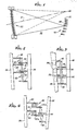
- the spectrum analyzer comprises an array of input tranducers, indicated generally by reference numeral 20, and an array of output transducers 22, both arrays being disposed on the surface of a piezoelectric substrate 24.
- An electrical input signal having a wide band of frequency components is applied to the input transcducer array 20, and the device functions to provide narrowband output signals from the output transducers 22.
- the principle of operation of the device is analagous to that of an optical diffraction grating.
- the input transducer array includes a relatively large number of individual transducers, each of which, at least in theory, functions as a point source of acoustic energy. If the substrate material is isotropic, the point sources of radiation give rise to circular wavefronts emanating from each input transducer. In practice, many SAW substrates are anisotropic, and the wavefront velocity is dependent on the direction of propagation.
- the transducers in the input array 20 are positioned on a circular arc, and the separate wavefronts from all of the transducers will reinforce each other at a zero-order focal point, indicated at 26, which is equidistant from all of the transducers.
- the zero-order focal point will be the same regardless of the frequency of the signals.
- there is a first-order focal point such as is shown at 28, where the accoustic waves from all of the input tranducers also combine to reinforce each other, but there is a one-wavelength difference in the path lengths to the focal point from any town adjacent transducers.
- the posi tion of this first-order focal point shifts laterally along a focal arc, indicated at 30.
- the output transducers 22 are arrayed along the focal arc 30, each having a relatively small aperture and being responsive to only a relatively narrow band of frequencies. In this manner, the SAW spectrum analyzer operates to provide a spectral set of narrowband output signals from a single wideband input signal.
- the device as described with reference to FIG. 1 suffers from a few significant disadvantages, such as lack of good frequency resolution. Also, devices constructed prior to this invention had to use anisotropic substrate materials for high frequency operation, and this required the use of cumbersome techniques to compensate for the differences in propagation velocity.
- the basic device illustrated in FIG. 1 is provided with a number of related improvements in the arrangement of its input transducers and its output transducers.
- a preferred form of the device employs an isotropic form of lithium niobate as the substrate.
- the isotropic substrate preferred in the structure of the invention is X-propagating, rotated Y-cut lithium niobate (LiNbO3), in which the Y-rotation angle is 121 degrees. It has been found that this particular cut provides a practically zero coefficient of anisotropy. In other words, the velocity of propagation is almost independent of direction, at least over a practical range of propagation directions. Moreover, the substrate still provides a desirably high coupling coefficient and relatively low attenuation losses.
- FIG. 2 shows how the input transducer array 20 is amplitude-weighted by varying the width of each transducer.
- the transducer structure illustrated includes two electrodes 34 and 36 arranged in a an approximately parallel relationship and having sum bars 38 and 40 extending toward each other in an overlapping relationship, referred to as an interdigital relationship. Extending from each of the sum bars are transducer elements or fingers 42. These are also arranged in an interdigital relationship. Each interdigital set of fingers 42 constitutes a transducer cell, and it will be seen that the three cells shown have different apertures or widths, i.e. the transducer fingers overlap by different amounts. This provides a continuously variable control over the transducer cell amplitude, so that the array 20 may be amplitude weighted in any desired manner to minimize sidelobes from the acoustic beam emanating from the array.
- FIG. 3 shows another type of amplitude weighting, employing series capacitance elements.
- two electrodes 46 and 48 are shown as substantially parallel.
- each electrode has sum bars 50 and 52 that are interdigital in form, but the sum bars 50 do not connect directly with the main electrode 46. Instead, they terminate in enlarged pads 54 beneath the electrode 46, and are separated therefrom by a dielectric layer, such as silicon dioxide (SiO2), which is not shown in FIG. 3.
- SiO2 silicon dioxide
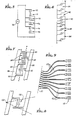
- FIG. 4 illustrates a form of resistive weighting for the same general purpose.
- there are two substantially parallel electrodes 56 and 58 each of which has sum bars 60 and 62.
- the sum bars 60 do not overlap the sum bars 62. Instead, they overlap subsidiary sum bars 60a, which are joined to the main sum bars 60 by relatively thin conductive strips 64.
- the subsidiary sum bars 60a overlap the opposing sum bars 62, and there are interdigital fingers 66 extending from both the sum bars 62 and the subsidiary sum bars 60a.
- the conductive strips 64 are used as adjustable resistive elements, and may be trimmed by laser or other methods, for any needed fine-tuning prior to completion of the fabrication process.
- FIG. 5 shows another technique for amplitude weighting of the input transducer array 20.
- Six transducer cells 70-75 are shown by way of example, connected to an input signal source 76.
- Transducers that are the first two in the array, i.e. those referred to by numerals 70 and 71, are connected in series with the signal source 76.
- the last two transducers 74 and 75 in the array are also connected in series.
- the two transducers 72 and 73 in the middle of the array are connected in parallel directly to the signal source 76. This provides a course form of amplitude weighting, since it will be seen that the amplitude resulting from the middle transducers 72 and 73 will be twice that of the outer transducers 70, 71, 74 and 75.
- FIG. 6 Another coarse form of amplitude weighting is shown in FIG. 6. Basically, transducers near the center of the array 20 are closely spaced as usual, as indicated at 80, but are spaced less closely toward the ends of the array. Numeral 82 indicates spaces in the array that would normally accommodate one additional transducer, and numeral 84 indicates spaces that would normally accommodate two additional transducers. In practice, these last-described coarse weighting techniques can be best applied in combination with another approach, such as aperture width weighting, for finetuning the array to provide a desired output pattern.
- the input transducer array 20 is modified in the manner shown in FIG. 7.
- a transducer cell is formed by fingers extending from oppposed sum bars, each of which contributes fingers to only one transducer cell.
- This geometric arrangement results in the side-by-side placement of sum bars or electrode branches of opposite polarities, as is readily apparent from FIG. 2.
- each sum bar contributes transducer fingers 94 in both directions, so that there is only one sum bar separating two adjacent transducer cells.
- FIG. 7 Another related aspect of the structure shown in FIG. 7 is in the non-overlapping placement of the electrodes and sum bars.
- transducer cells are formed without side-by-side placement of the the sum bars, but one electrode is placed in overlapping relation with the sum bars of the other electrode, which may pose capacitance problems at higher frequencies.
- the present structure not only avoids side-by-side placement of sum bars of opposite polarities, but also avoids overlapping of electrode elements of opposite polarities.
- the array transducer fingers 100 are made to conform with an arc, centered approximately at the intended point of origin 102 of the acoustic waves generated. Since each input transducer is intended to function as a point source of acoustic energy, the curvature of the transducer fingers more nearly approximates this ideal, since there is clearly a tendency for straight transducer fingers to favor propagation in a direction perpendicular to the fingers. The use of curved input transducer fingers results in reduced off-axis distortion and increased analyzer bandwidth.
- FIG. 9 illustrates a solution to this difficulty.
- the output signals are "fanned out" by waveguides 110, the inputs of which are arrayed along the focal arc of the device.
- the outputs of the waveguides may by conveniently more widely spaced, allowing ample room for conventional "in-line" interdigital transducers, indicated at 112.
- the waveguides 110 are acoustic waveguides. Electromag netic waveguides may be employed if output transducers are placed along the focal arc.
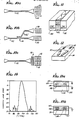
- FIG. 10a shows two output transducers 112 positioned at the output of a single waveguide 110.
- FIG. 10b shows an alternative arrangement in which a waveguide 110 is tapped at an acoustic waveguide coupler 114, forming an additional acoustic waveguide 110′ in parallel with the original one.
- the output transducers 112 are then positioned at the outputs of the waveguides 110 and 110′.
- a multistrip coupler 116 is positioned at the output of the waveguide 110, to provide a wider source of acoustic energy.
- Two transducers 112 are then placed in the path of acoustic waves emanating from the elements of the multistrip coupler. In all of these cases, the effect is to split the frequency band carried by the waveguide into two narrow and approximately equal portions, thereby further improving the frequency resolution.
- FIG. 11 shows in simplified form the structure of an acoustic waveguide. It includes a "slow" region 120, of lower wave velocity, sandwiched between two "fast" regions 122 of higher velocity.
- the slow region can take the form of a mass loaded strip, a slot, a shorting strip, an ion implantation region, or a diffusion region in the substrate.
- FIG> 12 shows a simplified output configuaration with surface-mounted acoustic waveguides 110, of metal of dielectric material, and two corres ponding output transducers.
- Other types of acoustic waveguides such as ridges or slots formed on the substrate, may be employed for the same purpose.
- FIGS. 13a and 13b show alternative forms of waveguides used at the output end of the analyzer.
- FIG. 13a shows a typical cross section of a hybrid stripline structure that can be mounted on the surface of the substrate 24 and used to transmit the energy focused at the focal arc.
- the stripline structure includes a layer 128 of dielectric material, such as silicon dioxide, sandwiched between two grounded conductive layers 130 and 132, and two conductors 134 buried in the dielectric layer.
- the structure shown in FIG. 13b includes a single thick layer 136 of grounded metal, with conductive strips 138 buried within the grounded layer but insulated from it by a dielectric cladding 140.
- FIG. 14 shows the center channel frequency response of the SAW spectrum analyzer of the invention, with the input transducer array 20 amplitude-weighted in accordance with Hamming function weighting.
- the amplitude weighting results in a first sidelobe that is about 55 dB below the center peak of the response.
- the present invention represents a significant advance in the field of surface acoustic wave devices.
- the invention provides improved frequency resolution, reduction of sidelobes in the focused acoustic beam, and higher dynamic range.
- the invention is not to be limited except as by the appended claims.
Landscapes
- Physics & Mathematics (AREA)
- Acoustics & Sound (AREA)
- Mathematical Physics (AREA)
- General Physics & Mathematics (AREA)
- Surface Acoustic Wave Elements And Circuit Networks Thereof (AREA)
Applications Claiming Priority (3)
| Application Number | Priority Date | Filing Date | Title |
|---|---|---|---|
| US06/580,575 US4499393A (en) | 1984-02-15 | 1984-02-15 | Surface acoustic wave spectrum analyzer |
| US580575 | 1984-02-15 | ||
| EP85300810A EP0161040B1 (fr) | 1984-02-15 | 1985-02-07 | Analyseur spectral employant des ondes superficielles acoustiques |
Related Parent Applications (1)
| Application Number | Title | Priority Date | Filing Date |
|---|---|---|---|
| EP85300810.0 Division | 1985-02-07 |
Publications (3)
| Publication Number | Publication Date |
|---|---|
| EP0309003A2 true EP0309003A2 (fr) | 1989-03-29 |
| EP0309003A3 EP0309003A3 (en) | 1990-12-27 |
| EP0309003B1 EP0309003B1 (fr) | 1994-12-07 |
Family
ID=26098173
Family Applications (1)
| Application Number | Title | Priority Date | Filing Date |
|---|---|---|---|
| EP19880117878 Expired - Lifetime EP0309003B1 (fr) | 1984-02-15 | 1985-02-07 | Analyseur de spectre d'ondes de surface acoustiques |
Country Status (1)
| Country | Link |
|---|---|
| EP (1) | EP0309003B1 (fr) |
Cited By (26)
| Publication number | Priority date | Publication date | Assignee | Title |
|---|---|---|---|---|
| EP3216231A4 (fr) * | 2014-11-07 | 2018-06-20 | Chirp Microsystems, Inc. | Guide d'ondes de boîtier pour capteur acoustique à compensation du temps de propagation électronique |
| WO2021130505A1 (fr) * | 2019-12-25 | 2021-07-01 | Ultraleap Limited | Structures de transducteur acoustique |
| US11098951B2 (en) | 2018-09-09 | 2021-08-24 | Ultrahaptics Ip Ltd | Ultrasonic-assisted liquid manipulation |
| US11169610B2 (en) | 2019-11-08 | 2021-11-09 | Ultraleap Limited | Tracking techniques in haptic systems |
| US11189140B2 (en) | 2016-01-05 | 2021-11-30 | Ultrahaptics Ip Ltd | Calibration and detection techniques in haptic systems |
| US11204644B2 (en) | 2014-09-09 | 2021-12-21 | Ultrahaptics Ip Ltd | Method and apparatus for modulating haptic feedback |
| US11276281B2 (en) | 2015-02-20 | 2022-03-15 | Ultrahaptics Ip Ltd | Algorithm improvements in a haptic system |
| US11307664B2 (en) | 2016-08-03 | 2022-04-19 | Ultrahaptics Ip Ltd | Three-dimensional perceptions in haptic systems |
| US11360546B2 (en) | 2017-12-22 | 2022-06-14 | Ultrahaptics Ip Ltd | Tracking in haptic systems |
| US11374586B2 (en) | 2019-10-13 | 2022-06-28 | Ultraleap Limited | Reducing harmonic distortion by dithering |
| US11378997B2 (en) | 2018-10-12 | 2022-07-05 | Ultrahaptics Ip Ltd | Variable phase and frequency pulse-width modulation technique |
| US11529650B2 (en) | 2018-05-02 | 2022-12-20 | Ultrahaptics Ip Ltd | Blocking plate structure for improved acoustic transmission efficiency |
| US11531395B2 (en) | 2017-11-26 | 2022-12-20 | Ultrahaptics Ip Ltd | Haptic effects from focused acoustic fields |
| US11543507B2 (en) | 2013-05-08 | 2023-01-03 | Ultrahaptics Ip Ltd | Method and apparatus for producing an acoustic field |
| US11550395B2 (en) | 2019-01-04 | 2023-01-10 | Ultrahaptics Ip Ltd | Mid-air haptic textures |
| US11553295B2 (en) | 2019-10-13 | 2023-01-10 | Ultraleap Limited | Dynamic capping with virtual microphones |
| US11550432B2 (en) | 2015-02-20 | 2023-01-10 | Ultrahaptics Ip Ltd | Perceptions in a haptic system |
| US20230054431A1 (en) * | 2020-01-16 | 2023-02-23 | Nederlandse Organisatie Voor Toegepast-Natuurwetenschappelijk Onderzoek Tno | Sound detection device |
| US11704983B2 (en) | 2017-12-22 | 2023-07-18 | Ultrahaptics Ip Ltd | Minimizing unwanted responses in haptic systems |
| US11727790B2 (en) | 2015-07-16 | 2023-08-15 | Ultrahaptics Ip Ltd | Calibration techniques in haptic systems |
| US11816267B2 (en) | 2020-06-23 | 2023-11-14 | Ultraleap Limited | Features of airborne ultrasonic fields |
| US11842517B2 (en) | 2019-04-12 | 2023-12-12 | Ultrahaptics Ip Ltd | Using iterative 3D-model fitting for domain adaptation of a hand-pose-estimation neural network |
| US11886639B2 (en) | 2020-09-17 | 2024-01-30 | Ultraleap Limited | Ultrahapticons |
| US11955109B2 (en) | 2016-12-13 | 2024-04-09 | Ultrahaptics Ip Ltd | Driving techniques for phased-array systems |
| US12373033B2 (en) | 2019-01-04 | 2025-07-29 | Ultrahaptics Ip Ltd | Mid-air haptic textures |
| US12517585B2 (en) | 2021-07-15 | 2026-01-06 | Ultraleap Limited | Control point manipulation techniques in haptic systems |
Family Cites Families (3)
| Publication number | Priority date | Publication date | Assignee | Title |
|---|---|---|---|---|
| DE3203679A1 (de) * | 1981-04-10 | 1982-11-18 | Licentia Patent-Verwaltungs-Gmbh, 6000 Frankfurt | Anordnung zur auswertung eines optischen strahles |
| GB2105939B (en) * | 1981-09-12 | 1985-10-02 | Marconi Co Ltd | A spectrum analyser and other apparatus for detecting at least one particular frequency component in an electrical signal |
| US4541687A (en) * | 1983-09-02 | 1985-09-17 | Trw Inc. | Signal processing system and method |
-
1985
- 1985-02-07 EP EP19880117878 patent/EP0309003B1/fr not_active Expired - Lifetime
Cited By (48)
| Publication number | Priority date | Publication date | Assignee | Title |
|---|---|---|---|---|
| US12345838B2 (en) | 2013-05-08 | 2025-07-01 | Ultrahaptics Ip Ltd | Method and apparatus for producing an acoustic field |
| US11624815B1 (en) | 2013-05-08 | 2023-04-11 | Ultrahaptics Ip Ltd | Method and apparatus for producing an acoustic field |
| US11543507B2 (en) | 2013-05-08 | 2023-01-03 | Ultrahaptics Ip Ltd | Method and apparatus for producing an acoustic field |
| US12204691B2 (en) | 2014-09-09 | 2025-01-21 | Ultrahaptics Ip Ltd | Method and apparatus for modulating haptic feedback |
| US11204644B2 (en) | 2014-09-09 | 2021-12-21 | Ultrahaptics Ip Ltd | Method and apparatus for modulating haptic feedback |
| US11768540B2 (en) | 2014-09-09 | 2023-09-26 | Ultrahaptics Ip Ltd | Method and apparatus for modulating haptic feedback |
| US11656686B2 (en) | 2014-09-09 | 2023-05-23 | Ultrahaptics Ip Ltd | Method and apparatus for modulating haptic feedback |
| EP3216231A4 (fr) * | 2014-11-07 | 2018-06-20 | Chirp Microsystems, Inc. | Guide d'ondes de boîtier pour capteur acoustique à compensation du temps de propagation électronique |
| US11830351B2 (en) | 2015-02-20 | 2023-11-28 | Ultrahaptics Ip Ltd | Algorithm improvements in a haptic system |
| US11550432B2 (en) | 2015-02-20 | 2023-01-10 | Ultrahaptics Ip Ltd | Perceptions in a haptic system |
| US11276281B2 (en) | 2015-02-20 | 2022-03-15 | Ultrahaptics Ip Ltd | Algorithm improvements in a haptic system |
| US12100288B2 (en) | 2015-07-16 | 2024-09-24 | Ultrahaptics Ip Ltd | Calibration techniques in haptic systems |
| US11727790B2 (en) | 2015-07-16 | 2023-08-15 | Ultrahaptics Ip Ltd | Calibration techniques in haptic systems |
| US11189140B2 (en) | 2016-01-05 | 2021-11-30 | Ultrahaptics Ip Ltd | Calibration and detection techniques in haptic systems |
| US12001610B2 (en) | 2016-08-03 | 2024-06-04 | Ultrahaptics Ip Ltd | Three-dimensional perceptions in haptic systems |
| US11307664B2 (en) | 2016-08-03 | 2022-04-19 | Ultrahaptics Ip Ltd | Three-dimensional perceptions in haptic systems |
| US11714492B2 (en) | 2016-08-03 | 2023-08-01 | Ultrahaptics Ip Ltd | Three-dimensional perceptions in haptic systems |
| US12271528B2 (en) | 2016-08-03 | 2025-04-08 | Ultrahaptics Ip Ltd | Three-dimensional perceptions in haptic systems |
| US11955109B2 (en) | 2016-12-13 | 2024-04-09 | Ultrahaptics Ip Ltd | Driving techniques for phased-array systems |
| US11531395B2 (en) | 2017-11-26 | 2022-12-20 | Ultrahaptics Ip Ltd | Haptic effects from focused acoustic fields |
| US11921928B2 (en) | 2017-11-26 | 2024-03-05 | Ultrahaptics Ip Ltd | Haptic effects from focused acoustic fields |
| US12347304B2 (en) | 2017-12-22 | 2025-07-01 | Ultrahaptics Ip Ltd | Minimizing unwanted responses in haptic systems |
| US12158522B2 (en) | 2017-12-22 | 2024-12-03 | Ultrahaptics Ip Ltd | Tracking in haptic systems |
| US11360546B2 (en) | 2017-12-22 | 2022-06-14 | Ultrahaptics Ip Ltd | Tracking in haptic systems |
| US11704983B2 (en) | 2017-12-22 | 2023-07-18 | Ultrahaptics Ip Ltd | Minimizing unwanted responses in haptic systems |
| US11883847B2 (en) | 2018-05-02 | 2024-01-30 | Ultraleap Limited | Blocking plate structure for improved acoustic transmission efficiency |
| US12370577B2 (en) | 2018-05-02 | 2025-07-29 | Ultrahaptics Ip Ltd | Blocking plate structure for improved acoustic transmission efficiency |
| US11529650B2 (en) | 2018-05-02 | 2022-12-20 | Ultrahaptics Ip Ltd | Blocking plate structure for improved acoustic transmission efficiency |
| US11098951B2 (en) | 2018-09-09 | 2021-08-24 | Ultrahaptics Ip Ltd | Ultrasonic-assisted liquid manipulation |
| US11740018B2 (en) | 2018-09-09 | 2023-08-29 | Ultrahaptics Ip Ltd | Ultrasonic-assisted liquid manipulation |
| US11378997B2 (en) | 2018-10-12 | 2022-07-05 | Ultrahaptics Ip Ltd | Variable phase and frequency pulse-width modulation technique |
| US12373033B2 (en) | 2019-01-04 | 2025-07-29 | Ultrahaptics Ip Ltd | Mid-air haptic textures |
| US11550395B2 (en) | 2019-01-04 | 2023-01-10 | Ultrahaptics Ip Ltd | Mid-air haptic textures |
| US11842517B2 (en) | 2019-04-12 | 2023-12-12 | Ultrahaptics Ip Ltd | Using iterative 3D-model fitting for domain adaptation of a hand-pose-estimation neural network |
| US11742870B2 (en) | 2019-10-13 | 2023-08-29 | Ultraleap Limited | Reducing harmonic distortion by dithering |
| US11553295B2 (en) | 2019-10-13 | 2023-01-10 | Ultraleap Limited | Dynamic capping with virtual microphones |
| US11374586B2 (en) | 2019-10-13 | 2022-06-28 | Ultraleap Limited | Reducing harmonic distortion by dithering |
| US12568341B2 (en) | 2019-10-13 | 2026-03-03 | Sim Ip Hxr Llc | Dynamic capping with virtual microphones |
| US12191875B2 (en) | 2019-10-13 | 2025-01-07 | Ultraleap Limited | Reducing harmonic distortion by dithering |
| US11169610B2 (en) | 2019-11-08 | 2021-11-09 | Ultraleap Limited | Tracking techniques in haptic systems |
| WO2021130505A1 (fr) * | 2019-12-25 | 2021-07-01 | Ultraleap Limited | Structures de transducteur acoustique |
| US12002448B2 (en) | 2019-12-25 | 2024-06-04 | Ultraleap Limited | Acoustic transducer structures |
| US11715453B2 (en) | 2019-12-25 | 2023-08-01 | Ultraleap Limited | Acoustic transducer structures |
| US20230054431A1 (en) * | 2020-01-16 | 2023-02-23 | Nederlandse Organisatie Voor Toegepast-Natuurwetenschappelijk Onderzoek Tno | Sound detection device |
| US11816267B2 (en) | 2020-06-23 | 2023-11-14 | Ultraleap Limited | Features of airborne ultrasonic fields |
| US12393277B2 (en) | 2020-06-23 | 2025-08-19 | Ultraleap Limited | Features of airborne ultrasonic fields |
| US11886639B2 (en) | 2020-09-17 | 2024-01-30 | Ultraleap Limited | Ultrahapticons |
| US12517585B2 (en) | 2021-07-15 | 2026-01-06 | Ultraleap Limited | Control point manipulation techniques in haptic systems |
Also Published As
| Publication number | Publication date |
|---|---|
| EP0309003B1 (fr) | 1994-12-07 |
| EP0309003A3 (en) | 1990-12-27 |
Similar Documents
| Publication | Publication Date | Title |
|---|---|---|
| EP0309003B1 (fr) | Analyseur de spectre d'ondes de surface acoustiques | |
| US4499393A (en) | Surface acoustic wave spectrum analyzer | |
| EP0184508B1 (fr) | Transducteur à ondes acoustiques de surface | |
| KR19990044685A (ko) | 탄성 표면파 장치를 위한 가감보정된 테이퍼변환기 | |
| US6791236B1 (en) | Method utilizing the saw velocity dispersion effect for weighting by shaping the electrode fingers of a saw interdigital transducer and apparatus produced thereby | |
| US5289073A (en) | Unidirectional surface acoustic wave transducer | |
| US4027946A (en) | Acousto-optic guided-light beam device | |
| US4827229A (en) | Broad band bulk acoustic wave spectrum analyzer/channelizer | |
| EP0031685B2 (fr) | Dispositif à ondes acoustiques de surface | |
| EP0579871A1 (fr) | Convolutionneur d'ondes acoustiques de surface | |
| US5818310A (en) | Series-block and line-width weighted saw filter device | |
| EP0106384B1 (fr) | Dispositif à ondes acoustiques de surface | |
| EP0270027B1 (fr) | Appareil déflecteur optique | |
| US4947073A (en) | Saw channelized filters | |
| US4541687A (en) | Signal processing system and method | |
| US4365220A (en) | Surface wave circuit device | |
| EP0153092A2 (fr) | Filtre passe bande à ondes acoustiques de surface | |
| JPH0450564B2 (fr) | ||
| EP0279678A2 (fr) | Ligne à retard à ondes de surface comportant des électrodes antiréfléchissantes | |
| US3968461A (en) | Acoustic surface-wave devices | |
| US4527866A (en) | Acousto-optic transducer | |
| JPH0778588B2 (ja) | 光偏向装置 | |
| Cheo | Thin-film waveguide devices | |
| US4737743A (en) | Single mode waveguide saw dispersive filter | |
| EP0117081A2 (fr) | Ligne à retard dispersive à ondes acoustiques de surface |
Legal Events
| Date | Code | Title | Description |
|---|---|---|---|
| PUAI | Public reference made under article 153(3) epc to a published international application that has entered the european phase |
Free format text: ORIGINAL CODE: 0009012 |
|
| 17P | Request for examination filed |
Effective date: 19881117 |
|
| AC | Divisional application: reference to earlier application |
Ref document number: 161040 Country of ref document: EP |
|
| AK | Designated contracting states |
Kind code of ref document: A2 Designated state(s): DE FR GB IT |
|
| PUAL | Search report despatched |
Free format text: ORIGINAL CODE: 0009013 |
|
| AK | Designated contracting states |
Kind code of ref document: A3 Designated state(s): DE FR GB IT |
|
| RHK1 | Main classification (correction) |
Ipc: G01R 23/17 |
|
| 17Q | First examination report despatched |
Effective date: 19940124 |
|
| ITF | It: translation for a ep patent filed | ||
| GRAA | (expected) grant |
Free format text: ORIGINAL CODE: 0009210 |
|
| AC | Divisional application: reference to earlier application |
Ref document number: 161040 Country of ref document: EP |
|
| AK | Designated contracting states |
Kind code of ref document: B1 Designated state(s): DE FR GB IT |
|
| REF | Corresponds to: |
Ref document number: 3587959 Country of ref document: DE Date of ref document: 19950119 |
|
| PGFP | Annual fee paid to national office [announced via postgrant information from national office to epo] |
Ref country code: FR Payment date: 19950214 Year of fee payment: 12 |
|
| ET | Fr: translation filed | ||
| PLBE | No opposition filed within time limit |
Free format text: ORIGINAL CODE: 0009261 |
|
| STAA | Information on the status of an ep patent application or granted ep patent |
Free format text: STATUS: NO OPPOSITION FILED WITHIN TIME LIMIT |
|
| PG25 | Lapsed in a contracting state [announced via postgrant information from national office to epo] |
Ref country code: FR Effective date: 19951031 |
|
| 26N | No opposition filed | ||
| REG | Reference to a national code |
Ref country code: FR Ref legal event code: ST |
|
| PGFP | Annual fee paid to national office [announced via postgrant information from national office to epo] |
Ref country code: GB Payment date: 19990108 Year of fee payment: 15 |
|
| PGFP | Annual fee paid to national office [announced via postgrant information from national office to epo] |
Ref country code: DE Payment date: 19990226 Year of fee payment: 15 |
|
| PG25 | Lapsed in a contracting state [announced via postgrant information from national office to epo] |
Ref country code: GB Free format text: LAPSE BECAUSE OF NON-PAYMENT OF DUE FEES Effective date: 20000207 |
|
| GBPC | Gb: european patent ceased through non-payment of renewal fee |
Effective date: 20000207 |
|
| PG25 | Lapsed in a contracting state [announced via postgrant information from national office to epo] |
Ref country code: DE Free format text: LAPSE BECAUSE OF NON-PAYMENT OF DUE FEES Effective date: 20001201 |