EP0309250B1 - Circuit de détection à corrélation utilisable en basse fréquence - Google Patents
Circuit de détection à corrélation utilisable en basse fréquence Download PDFInfo
- Publication number
- EP0309250B1 EP0309250B1 EP88308815A EP88308815A EP0309250B1 EP 0309250 B1 EP0309250 B1 EP 0309250B1 EP 88308815 A EP88308815 A EP 88308815A EP 88308815 A EP88308815 A EP 88308815A EP 0309250 B1 EP0309250 B1 EP 0309250B1
- Authority
- EP
- European Patent Office
- Prior art keywords
- error
- converted
- data
- quadrature
- phase
- Prior art date
- Legal status (The legal status is an assumption and is not a legal conclusion. Google has not performed a legal analysis and makes no representation as to the accuracy of the status listed.)
- Expired - Lifetime
Links
- 230000003111 delayed effect Effects 0.000 claims description 40
- 230000003044 adaptive effect Effects 0.000 claims description 19
- 230000005540 biological transmission Effects 0.000 claims description 12
- 238000001914 filtration Methods 0.000 claims description 4
- 238000001514 detection method Methods 0.000 description 10
- 238000011084 recovery Methods 0.000 description 6
- 238000010586 diagram Methods 0.000 description 5
- 230000001427 coherent effect Effects 0.000 description 3
- 230000015556 catabolic process Effects 0.000 description 1
- 230000000295 complement effect Effects 0.000 description 1
- 230000008878 coupling Effects 0.000 description 1
- 238000010168 coupling process Methods 0.000 description 1
- 238000005859 coupling reaction Methods 0.000 description 1
- 230000003247 decreasing effect Effects 0.000 description 1
- 238000006731 degradation reaction Methods 0.000 description 1
- 230000001934 delay Effects 0.000 description 1
- 229910044991 metal oxide Inorganic materials 0.000 description 1
- 150000004706 metal oxides Chemical class 0.000 description 1
- 239000004065 semiconductor Substances 0.000 description 1
Images


Classifications
-
- H—ELECTRICITY
- H04—ELECTRIC COMMUNICATION TECHNIQUE
- H04L—TRANSMISSION OF DIGITAL INFORMATION, e.g. TELEGRAPHIC COMMUNICATION
- H04L27/00—Modulated-carrier systems
- H04L27/01—Equalisers
Definitions
- This invention relates to a correlation detecting circuit for use in an adaptive equalizer system and, more particularly, to a correlation detecting circuit for use in an adaptive equalizer system for a digital radio transmission system.
- an adaptive equalizer system of the type described is supplied through a transmission path with a received signal subjected to modulation at a modulation rate.
- the received signal carries a transmission data sequence digitized by a reference clock signal.
- the reference clock signal has a reference clock frequency which is equal to the modulation rate.
- the modulation may be, for example, quadrature amplitude modulation (QAM).
- QAM quadrature amplitude modulation
- the received signal has a waveform subject to a distortion which results from degradation of a characteristic in the transmission path and interruption in the transmission path.
- the adaptive equalizer system serves to equalize the distortion of the waveform, as well known in the art.
- the adaptive equalizer system comprises a transversal filter for filtering the received signal into an equalized signal in response to a plurality of controllable tap gains and a demodulator for demodulating the equalized signal into a reproduced clock signal, a reproduced data sequence, and a digital error signal.
- the reproduced clock signal is a reproduction of the reference clock signal.
- the reproduced data sequence is a reproduction of the transmission data sequence.
- the digital error signal is related to the reproduced data sequence.
- the adaptive equalizer system further comprises a gain control circuit responsive to the reproduced clock signal, to the reproduced data sequence, and to the digital error signal for controlling the controllable tap gains by the use of an equalizing algorithm.
- the equalizing algorithm is, for example, a zero forcing (ZF) algorithm.
- the gain control circuit comprises a correlation detecting circuit and an integrating circuit.
- the correlation detecting circuit comprises a delaying circuit and an Exclusive logic circuit.
- the delaying circuit is for delaying the reproduced data sequence and the digital error signal to produce a delayed data sequence and a delayed error signal in synchronism with the reproduced clock signal.
- the delaying circuit comprises a plurality of flip flops.
- the delayed data sequence, the delayed error signal, the reproduced data sequence, and the digital error signal are supplied to the Exclusive logic circuit as a plurality of input signals.
- the Exclusive logic circuit is for carrying out an exclusive logic operation on the input signals to produce a plurality of correlation signals which represent cross-correlation between the reproduced data sequence and the digital error signal.
- the Exclusive logic circuit comprises a plurality of exclusive logic gates. Each of the exclusive logic gates is either an Exclusive OR gate or an Exclusive NOR gate.
- the integrating circuit is for integrating the correlation signals to produce a plurality of integrated signals as the controllable tap gains.
- a conventional correlation detecting circuit is implemented either as an integrated circuit (IC) or a large-scale integrated circuit (LSI).
- IC integrated circuit
- LSI large-scale integrated circuit
- Each of the IC and LSI comprises a plurality of complementary metal oxide semiconductor (CMOS) circuits.
- CMOS complementary metal oxide semiconductor
- the CMOS circuit has a low power consumption.
- the CMOS circuit has a maximum CMOS operation speed which is about thirty-five in terms of megahertz and is lower than that of other circuits, for example, a current mode logic (CML) circuit. Therefore, the conventional correlation detecting circuit can not be used in the adaptive equalizer system supplied with the received signal of the modulation rate which is higher than the maximum CMOS operation speed if the conventional correlation detecting circuit comprises the CMOS circuits.
- CML current mode logic
- the adaptive equalizer system is, for example, for four-by-four quadrature amplitude modulation, namely, 16-QAM, and is supplied with the received signal of a bit transfer rate which is equal to two hundreds megabits per second, the modulation rate is equal to fifty megahertz and is higher than the maximum CMOS operation speed.
- the conventional correlation detecting circuit must be composed of discrete integrated circuits, each of which comprises a plurality of CML circuits.
- the conventional correlation detecting circuit is disadvantageous in that it is impossible to render the conventional correlation detecting circuit compact and that it is impossible to have a low power consumption.
- a correlation detecting circuit to which this invention is applicable is for use in an adaptive equalizer system comprising a transversal filter for filtering a received signal into an equalized signal in response to a plurality of controllable tap gains and a demodulator for demodulating the equalized signal into a reproduced clock signal, a reproduced data sequence, and a digital error signal.
- the received signal carries a transmission data sequence digitized by a reference clock signal.
- the reproduced clock signal is a reproduction of the reference clock signal.
- the reproduced data sequence is a reproduction of the transmission data sequence.
- the digital error signal is related to the reproduced data sequence.
- the correlation detecting circuit includes logic operation carrying out means for carrying out an exclusive logic operation on a plurality of input signals derived from the reproduced clock signal, the reproduced data sequence, and the digital error signal to produce a plurality of correlation signals which represent cross-correlation between the reproduced data sequence and the digital error signal and are collectively used in controlling the controllable tap gains.
- the correlation detecting circuit comprises divider means for frequency dividing the reproduced clock signal to produce a divided clock signal and serial-parallel converting means coupled to the divider means and responsive to the digital error signal and to the reproduced data sequence for converting the digital error signal and the reproduced data sequence into the input signals in synchronism with the divided clock signal.
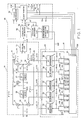
- the adaptive equalizer system is supplied with a received signal IN of an intermediate frequency band.
- the received signal IN is assumed to be subjected to four-by-four quadrature amplitude modulation (16-QAM) at a predetermined modulation rate.
- the predetermined modulation rate is, for example, equal to fifty megahertz.
- the received signal IN is modulated by or carries a transmission data sequence digitized by a reference clock signal.
- the reference clock signal has a reference clock frequency which is equal to the predetermined modulation rate.
- the adaptive equalizer system comprises a transversal filter 20 for filtering the received signal IN into an equalized signal OUT in response to a plurality of controllable tap gains which may be specified by C(-1), C(0), and C(+1).
- the equalized signal OUT is also subjected to four-by-four quadrature amplitude modulation like the received signal IN but is equalized by the transversal filter 20.
- the illustrated transversal filter 20 has three taps. A central one of the three taps may be called a central or a first tap 21. The remaining ones of the taps are depicted on the lefthand and the righthand sides of the central tap 21 and may be called second and third taps 22 and 23, respectively.
- the second and the third taps 22 and 23 may be referred to as first and second additional taps.
- First and second delay units 26 and 27 are placed between the second and the first taps 22 and 21 and between the first and the third taps 21 and 23, respectively.
- Each of the first and the second delay units 26 and 27 provides a delay which is substantially equal to a reciprocal of the modulation rate.
- the received signal IN is delivered to the second tap 22 as a first one of additional tap signals and successively delayed by the first and the second delay units 26 and 27 to be produced as a central tap signal and a second additional tap signal which are sent to the first and the third taps 21 and 23, respectively.
- the second, the first, and the third taps 22, 21, and 23 be specified by consecutive numbers of (-1), 0, and (+1), respectively, taking the successive delays into consideration.
- the first additional tap signal appearing as the (-1) tap 22 may be specified by S(-1).
- the central and the second additional tap signals may be specified by S(0) and S(+1), respectively.
- the received signal IN includes an in-phase and a quadrature phase component.
- the in-phase and the quadrature phase components are individually processed with reference to the central tap signal S(0). More specifically, the first additional tap signal S(-1) is delivered to a first in-phase multiplier 31 and a first quadrature multiplier 32.
- the second additional tap signal S(+1) is delivered to a second in-phase multiplier 33 and a second quadrature multiplier 34 in a manner to be described later.
- the central tap signal S(0) is given to a central in-phase multiplier 35 alone because no quadrature phase component is present in the central tap signal S(0).
- Each of the multipliers 31 to 35 may be referred to as a weighting circuit.
- the controllable tap gains C(0), C(-1), and C(+1) are produced by a gain control circuit 38 as will later be described in detail.
- the controllable tap gains C(0), C(-1), and C(+1) may be referred to as a central complex control signal, first and second complex control signals, respectively.
- the central complex control signal C(0) consists of a real part alone and is therefore represented by r(0) in Fig. 1.
- each of the first and the second complex control signals C(-1) and C(+1) consists of a real part and an imaginary part represented by r and d, respectively.
- the first complex control signal C(-1) is specified by a combination of r(-1) and d(-1) while the second complex control signal C(+1), a combination of r(1) and d(1).
- the real and the imaginary parts r(-1) and d(-1) of the first complex control signal C(-1) are delivered from the gain control circuit 38 to the first in-phase and the first quadrature multipliers 31 and 32, respectively.
- the real and the imaginary parts r(1) and d(1) of the second complex control signal C(+1) are delivered to the second in-phase and the second quadrature multipliers 33 and 34, respectively.
- the central complex control signal C(0) or r(0) is sent to the central in-phase multiplier 35 in a usual manner.
- the first in-phase and the first quadrature multipliers 31 and 32 supply first and second adders 41 and 42 with a first controlled in-phase component S′(-1) and a first controlled quadrature component S ⁇ (-1), respectively.
- the second in-phase and the second quadrature multipliers 33 and 34 supply the first and the second adders 41 and 42 with a second controlled in-phase component and a second controlled quadrature component which are represented by S′(+1) and S ⁇ (+1), respectively.
- Each of the first and the second in-phase components may be named a first controlled signal while each of the first and the second quadrature components is named a second controlled signal.
- a central controlled in-phase component S′(0) is sent from the central in-phase multiplier 35 to the first adder 41.
- the first and the second adders 41 and 42 carry out addition to produce an in-phase signal RS and a quadrature signal IS representative of results of the addition, respectively.
- the in-phase and the quadrature signals RS and IS may be called first and second processed signals, respectively.
- the first and the second adders 41 and 42 may be referred to as first and second processing circuits, respectively.
- the in-phase and the quadrature signals RS and IS are combined together by a coupling circuit 51 into a coupled signal with a quadrature phase relation kept between the in-phase and the quadrature signals RS and IS.
- the coupled signal is sent as the equalized signal OUT to a demodulator 55.
- the demodulator 55 comprises a coherent detector 56 responsive to the equalized signal OUT and to a recovered carrier wave supplied from a carrier recovery circuit 57.
- the coherent detector 56 carries out coherent detection with reference to the recovered carrier wave to produce a demodulated baseband signal.
- the demodulated baseband signal consists of an in-phase and a quadrature component represented by Bp and Bq, respectively.
- the in-phase and the quadrature components Bp and Bq have an in-phase and a quadrature level, respectively.
- a clock generator 59 delivers a reproduced clock signal CLK to both of the gain control circuit 38 and a discriminator 61.
- the reproduced clock signal CLK is a reproduction of the reference clock signal.
- the discriminator 61 produces a reproduced data sequence D.
- the reproduced data sequence is a reproduction of the transmission data sequence.
- the reproduced data sequence D consists of in-phase data components Dp and D′p and of quadrature data components Dq and D′q.
- the in-phase data components Dp and D′p represent the in-phase level of the in-phase component Bp of the demodulated baseband signal.
- the quadrature data components Dq and D′q represent the quadrature level of the quadrature component Bq of the demodulated baseband signal.
- the discriminator 61 also produces a digital error signal E.
- the digital error signal E is related to the reproduced data sequence D.
- the digital error signal E consists of an in-phase and a quadrature error component Ep and Eq which correspond to the in-phase and the quadrature data components Dp and Dq, respectively.
- a discriminator 61 may be a decision circuit described in the above-referenced United States patent and will therefore not be described any longer.
- the carrier recovery circuit 57 additionally produces the recovered carrier wave in response to the in-phase and the quadrature components Bp and Bq of the demodulated baseband signal.
- the carrier recovery circuit 57 is coupled to an asynchronous detection circuit 62.
- the asynchronous detection circuit 62 monitors the carrier recovery circuit 57 to detect an asynchronous state of the equalizer and to produce an asynchronous state signal ASY representative of the asynchronous state when the asynchronous detection circuit 62 detects the asynchronous state.
- the in-phase and the quadrature error components Ep and Eq of the digital error signal E and the in-phase and the quadrature data components Dp and Dq of the reproduced data sequence D are delivered from the demodulator 55 to the gain control circuit 38 together with the reproduced clock signal CLK and the asynchronous state signal ASY.
- the gain control circuit 38 controls the controllable tap gains C(j) by the use of a zero forcing (ZF) algorithm where j represents a tap number, such as 0, (-1), and (+1). It will be assumed that a k-th time k is prior to a (k+1)-th time (k+1) by a repetition period of the reproduced clock signal CLK.
- ZF zero forcing
- the controllable tap gains C(j, k+1) have real and imaginary parts r(j, k+1) and d(j, k+1) which are given by: where the symbol ⁇ is used as an Exclusive-OR operator and the symbol ⁇ is used as an Exclusive-NOR operator.
- the gain control circuit 38 comprises a correlation detecting circuit 63 and an integrating circuit 64.
- the correlation detecting circuit 63 is for finding out cross-correlation between the reproduced data sequence D(m) and the digital error signal E(m) to produce a plurality of correlation signals.
- the integrating circuit 64 is for integrating the correlation signals to produce a plurality of integrated signals as the controllable tap gains C(j).
- the illustrated correlation detecting circuit comprises a delaying circuit 65 and an Exclusive logic circuit 70.
- the delaying circuit 65 is for delaying the reproduced data sequence D(m) and the digital error signal E(m) to produce a delayed data sequence D(m-1) and a delayed error signal E(m-1) in synchronism with the reproduced clock signal CLK.
- the delayed data sequence D(m-1) and the delayed error signal E(m-1) are delayed by one repetition period of the reproduced clock signal CLK relative to the reproduced data sequence D(m) and the digital error signal E(m), respectively.
- the delaying circuit 65 comprises first through fourth flip flops 66, 67, 68, and 69.
- the delayed clock signal CLK is delivered to the flip flops 66 through 69.
- the first flip flop 66 is for delaying an in-phase error component Ep(m) of the digital error signal E(m) to produce a delayed in-phase error component Ep(m-1) of the delayed error signal E(m-1) in synchronism with the reproduced clock signal CLK.
- the second flip flop 67 is for delaying a quadrature error component Eq(m) of the digital error signal E(m) to produce a delayed quadrature error component Eq(m-1) of the delayed error signal E(m-1) in synchronism with the reproduced clock signal CLK.
- the third and the fourth flip flop 68 and 69 are for delaying in-phase and quadrature data components Dp(m) and Dq(m) of the reproduced data sequence D(m) to produce delayed in-phase and delayed quadrature data components Dp(m-1) and Dq(m-1) of the delayed data sequence D(m-1), respectively, in synchronism with the reproduced clock signal CLK.
- the delayed data sequence D(m-1), the delayed error signal E(m-1), the reproduced data sequence D(m), and the digital error signal E(m) are supplied to the Exclusive logic circuit 70 as a plurality of input signals.
- the Exclusive logic circuit 70 is for carrying out an exclusive logic operation on the input signals to produce the correlation signals.
- the Exclusive logic circuit 70 comprises first through ninth Exclusive-OR gates 71, 72, 73, 74, 75, 76, 77, 78, and 79, and first through third Exclusive-NOR gates 81, 82, and 83. More particularly, the first Exclusive-OR gate 71 carries out an exclusive OR operation on the in-phase error component Ep(m) and the in-phase data component Dp(m) to produce a first correlation signal Pr(0).
- the second Exclusive-OR gate 72 carries out an exclusive OR operation on the quadrature error component Eq(m) and the quadrature data component Dq(m) to produce a second correlation signal Qr(0).
- the third Exclusive-OR gate 73 carries out an exclusive OR operation on the quadrature error component Eq(m) and the in-phase data component Dp(m) to produce a third correlation signal Qd(0).
- the first Exclusive-NOR gate 81 carries out an exclusive NOR operation on the in-phase error component Ep(m) and the quadrature data component Dq(m) to produce a fourth correlation signal Pd(0).
- the correlation signals except for the third and the fourth correlation signals Qd(0) and Pd(0) are supplied to the integrating circuit 64.
- the in-phase and the quadrature components Bp and Bq of the demodulated baseband signal are supplied to the carrier recovery circuit 57 as mentioned above, the in-phase and the quadrature components Bp and Bq of the demodulated baseband signal may not be always supplied to the carrier recovery circuit 57.
- the third and the fourth correlation signals Qd(0) and Pd(0) is used instead of the in-phase and the quadrature components Bp and Bq of the demodulated baseband signal.
- the integrating circuit 64 comprises first through fifth resettable integrators 91, 92, 93, 94, and 95.
- the first resettable integrator 91 is coupled through first and second registers 101 and 102 to the first and the second Exclusive-OR gates 71 and 72.
- the second resettable integrator 92 is coupled through third and fourth registers 103 and 104 to the fourth and the fifth Exclusive-OR gates 74 and 75.
- the third resettable integrator 93 is coupled through fifth and sixth registers 105 and 106 to the sixth Exclusive-OR gate 76 and the second Exclusive-NOR gate 82.
- the fourth resettable integrator 94 is coupled through seventh and eighth registers 107 and 108 to the seventh and eighth Exclusive-OR gates 77 and 78.
- the fifth resettable integrator 95 is coupled through ninth and tenth registers 109 and 110 to the ninth Exclusive-OR gate 79 and the third Exclusive-NOR gate 83.
- a pair of the first and the second registers 101 and 102 are for combining the first correlation signal Pr(0) and the second correlation signal Qr(0) to produce a first combined signal ER(0). Therefore, the first combined signal ER(0) is given by:
- another pair of the third and the fourth registers 103 and 104 are for combining the fourth correlation signal Pr(-1) and the fifth correlation signal Qr(-1) to produce a second combined signal ER(-1) which is given by:
- pairs of the fifth and the sixth registers 105 and 106, the seventh and the eighth registers 107 and 108, and the ninth and the tenth registers 109 and 110 produce third, fourth, and fifth combined signals EI(-1), ER(1), and EI(1), respectively, which are given by:
- the first through the fifth resettable integrators 91 to 95 are coupled to the asynchronous detecting circuit 62.
- the first resettable integrators 91 is reset into a logic "1" level and is kept at the logic "1" level.
- Each of the remaining integrators 92 to 95 is reset into a logic "0" level.
- each of the integrators 91 to 95 works out a time average of each combined signal ER(0), ER(-1), EI(-1), ER(1), and EI(1) to remove an unnecessary noise component from each combined signal.
- the first through the fifth integrators 92 to 95 produce the controllable tap gains C(0), C(-1), and C(+1).
- the first through the tenth registers 101 to 110 are for use in combining each pair of the correlation signals as mentioned above.
- OR gates may be used instead of the first through the tenth registers 101 to 110.
- controllable tap gains C(0), C(-1), and C(+1) are determined by the zero forcing algorithm given by Equation (1).
- the conventional correlation detecting circuit operates in synchronism with the reproduced clock signal CLK.
- the reproduced clock signal CLK has a clock frequency which is equal to the modulation rate. Therefore, the conventional correlation detecting circuit is disadvantageous as pointed out heretobefore.
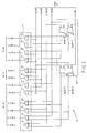
- a correlation detecting circuit 63′ according to a first embodiment of this invention comprises similar parts designated by like reference numerals.
- the illustrated correlation detecting circuit 63′ is for use in the adaptive equalizer system as shown in Fig. 1.
- the illustrated correlation detecting circuit 63′ comprises a divider 111 for frequency dividing the reproduced clock signal CLK by a factor 1/2.
- the divider 111 produces a divided clock signal CLK/2.
- the divided clock signal CLK/2 has a divided clock frequency which is equal to a half of the clock frequency.
- the divider 111 is coupled to a serial-parallel converter 120 supplied with the digital error signal E(m) and the reproduced data sequence D(m).
- the serial-parallel converter 120 is for converting the digital error signal E(m) and the reproduced data sequence D(m) into first and second converted error signals E(2n) and E(2n-1) and first and second converted data sequences D(2n) and D(2n-1) in synchronism with the divided clock signal CLK/2.
- the first and the second converted error signals E(2n) and E(2n-1) and the first and the second converted data sequences D(2n) and D(2n-1) are delivered through lines 130 to the Exclusive logic circuit 70 collectively as the input signals.
- the lines 130 act as a supplying arrangement for supplying the converted error signals and the converted data sequences to the Exclusive logic circuit 70.
- the serial-parallel converter 120 comprises first through fourth serial-parallel converting units 121, 122, 123, and 124.
- the first serial-parallel converting unit 121 is for converting the in-phase error component Ep(m) of the digital error signal E(m) into first and second parallel in-phase error components Ep(2n) and Ep(2n-1) in synchronism with the divided clock signal CLK/2.
- the second serial-parallel converting unit 122 is for converting the quadrature error component Eq(m) of the digital error signal E(m) into first and second parallel quadrature error components Eq(2n) and Eq(2n-1) in synchronism with the divided clock signal CLK/2.
- the first and the second parallel in-phase error components Ep(2n) and Ep(2n-1) are delivered through the lines 130 to the Exclusive logic circuit 70 as converted in-phase error components of the first and the second converted error signals E(2n) and E(2n-1).
- the first and the second parallel quadrature error components Eq(2n) and Eq(2n-1) are delivered through the lines 130 to the Exclusive logic circuit 70 as the converted quadrature error components of the first and the second converted error signals E(2n) and E(2n-1).
- the first and the second serial-parallel converting units 121 and 122 will be called in-phase and quadrature error serial-parallel converting arrangements, respectively.
- the third serial-parallel converting unit 123 is for converting the in-phase data component Dp(m) of the reproduced data sequence D(m) into first and second parallel in-phase data components Dp(2n) and Dp(2n-1) in synchronism with the divided clock signal CLK/2.
- the fourth serial-parallel converting unit 124 is for converting the quadrature data component Dq(m) of the reproduced data sequence D(m) into first and second parallel quadrature data components Dq(2n) and Dq(2n-1) in synchronism with the divided clock signal CLK/2.
- the first and the second parallel in-phase data components Dp(2n) and Dp(2n-1) are delivered through the lines 130 to the Exclusive logic circuit 70 as converted in-phase data components of the first and the second converted data sequences D(2n) and D(2n-1).
- the first and the second parallel quadrature data components Dq(2n) and Dq(2n-1) are delivered through the lines 130 to the Exclusive logic circuit 70 as converted quadrature data components of the first and the second converted data sequences D(2n) and D(2n-1).
- the third and the fourth serial-parallel converting units 123 and 124 will be called in-phase and quadrature data serial-parallel converting arrangements, respectively.
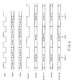
- the reproduced clock signal CLK is indicated along a first or top line.
- Second and third lines show the digital error signal E(m) and the reproduced data sequence D(m), respectively.
- the divided clock signal CLK/2 is indicated along a fourth line.
- Fifth through eighth lines show the first and the second converted error signals E(2n) and E(2n-1) and the first and the second converted data sequences D(2n) and D(2n-1).
- the digital error signal E(m) comprises a series of error elements such as a (2k-1)-th error element E(2k-1) of a (2k-1)-th time slot (2k-1), a 2k-th error element E(2k) of a 2k-th time slot 2k, a (2k+1)-th error element E(2k+1) of a (2k+1)-th time slot (2k+1), where k represents an integer.
- the reproduced data sequence D(m) comprises a series of data elements such as a (2k-1)-th data element D(2k-1) of the (2k-1)-th time slot (2k-1), a 2k-th data element D(2k) of the 2k-th time slot 2k, a (2k+1)-th data element D(2k+1) of the (2k+1)-th time slot (2k+1).
- the first converted error signal E(2n) comprises a series of converted error elements having time slots each of which is equal in number to an even number such as a (2k-2)-th error element E(2k-2) of a (2k-2)-th time slot (2k-2), the 2k-th error element E(2k) of the 2k-th time slot 2k, a (2k+2)-th error element E(2k+2) of a (2k+2)-th time slot (2k+2).
- the second converted error signal E(2n-1) comprises a series of converted error elements having time slots each of which is equal in number to an odd number such as a (2k-3)-th error element E(2k-3) of a (2k-3)-th time slot (2k-3), the (2k-1)-th error element E(2k-1) of the (2k-1)-th time slot (2k-1), the (2k+1)-th error element E(2k+1) of the (2k+1)-th time slot (2k+1).
- the first converted data sequence D(2n) comprises a series of converted data elements having time slots each of which is equal in number to the even number such as a (2k-2)-th data element D(2k-2) of the (2k-2)-th time slot (2k-2), the 2k-th data element D(2k) of the 2k-th time slot 2k, a (2k+2)-th data element D(2k+2) of the (2k+2)-th time slot (2k+2).
- the second converted data sequence D(2n-1) comprises a series of converted data elements having time slots each of which is equal in number to the odd number such as a (2k-3)-th data element D(2k-3) of the (2k-3)-th time slot (2k-3), the (2k-1)-th data element D(2k-1) of the (2k-1)-th time slot (2k-1), the (2k+1)-th data element D(2k+1) of the (2k+1)-th time slot (2k+1).
- the converted in-phase error component Ep(2n) of the first converted error signal E(2n) is supplied to the first and the seventh Exclusive-OR gates 71 and 77 and the first and the third Exclusive-NOR gates 81 and 83.
- the converted in-phase error component Ep(2n-1) of the second converted error signal E(2n-1) is supplied to the fourth Exclusive-OR gate 74 and the second Exclusive-NOR gate 82.
- the converted quadrature error component Eq(2n) of the first converted error signal E(2n) is supplied to the second, the third, the eighth, and the ninth Exclusive-OR gates 72, 73, 78, and 79.
- the converted quadrature error component Eq(2n-1) of the second converted error signal E(2n-1) is supplied to the fifth and the sixth Exclusive-OR gates 75 and 76.
- the converted in-phase data component Dp(2n) of the first converted data sequence D(2n) is supplied to the first, the third, the fourth, and the sixth Exclusive-OR gates 71, 73, 74, and 76.
- the converted in-phase data component Dp(2n-1) of the second converted data sequence D(2n-1) is supplied to the seventh and the ninth Exclusive-OR gates 77 and 79.
- the converted quadrature data component Dq(2n) of the first converted data sequence D(2n) is supplied to the second and the fifth Exclusive-OR gates 72 and 75 and the first and the second Exclusive-NOR gates 81 and 82.
- the converted quadrature data component Dq(2n-1) of the second converted data sequence D(2n-1) is supplied to the eighth Exclusive-OR gate 78 and the third Exclusive-NOR gate 83.
- the gain control circuit 38 produces controllable tap gains C(j, k+1) given by: where H′ represents a positive integer.
- the positive integer H′ corresponds to a time constant of the integrating circuit 64.
- the time constant is generally long.
- the illustrated correlation detecting circuit 63′ has an operation speed which is equal to the divided clock frequency except for the divider 111. If the operation speed is not higher than a maximum CMOS operation speed, the correlation detecting circuit 63′ can be formed, except for the divider 111, by an LSI consisting of CMOS circuits. Accordingly, it is possible to make the correlation detecting circuit 63′ have a small size and a low power consumption.
- the transversal filter has K taps where K represents a predetermined positive integer which is equal to (2M+1) where M represents a first predetermined natural number.
- the divider 111 is for dividing the reproduced clock signal CLK by a factor 1/N where N represents a second predetermined natural number which is not less than the first predetermined natural number M plus one.
- the serial-parallel converter 120 produces first through L-th converted error signals and first through L-th converted data sequences where L represents a third predetermined natural number which is equal to the second predetermined natural number N.
- the demodulator 55 produces an in-phase and a quadrature error component of the digital error signal, and an in-phase and a quadrature component of the reproduced data sequence.
- the Exclusive logic circuit 70 comprises a plurality of exclusive logic gates which are equal in number to four times the predetermined positive integer K. Each of the exclusive logic gates is responsive to a selected one of converted in-phase and quadrature error components of the converted error signals and to a selected one of converted in-phase and quadrature data components of the converted data sequences for producing a selected one of the correlation signals.
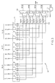
- a correlation detecting circuit 63a according to a second embodiment of this invention comprises similar parts designated by like reference numerals.
- the illustrated correlation detecting circuit 63a is for use in the adaptive equalizer system in which the transversal filter has seven taps.
- the correlation detecting circuit 63a comprises a serial-parallel converter 120a coupled to the divider 111 and supplied with the digital error signal E(m) and the reproduced data sequence D(m).
- the serial-parallel converter 120a is for converting the digital error signal E(m) and the reproduced data sequence D(m) into first through fourth converted error signals E(2n), E(2n-1), E(2n-2), and E(2n-3) and first through fourth converted data sequences D(2n), D(2n-1), D(2n-2), and D(2n-3) in synchronism with the divided clock signal CLK/2.
- the first through the fourth converted error signals E(2n) to E(2n-3) and the first through the fourth converted data sequences D(2n) to D(2n-3) are delivered through lines 130a to an Exclusive logic circuit 70a collectively as the input signals.
- the serial-parallel converter 120a comprises first through eighth flip flops 131, 132, 133, 134, 135, 136, 137, and 138 in addition to the first through the fourth serial-parallel converting units 121 to 124.
- the first and the second flip flops 131 and 132 are coupled to the first serial-parallel converting unit 121 for delaying the first and the second parallel in-phase error components Ep(2n) and Ep(2n-1) to produce first and second delayed in-phase error components Ep(2n-2) and Ep(2n-3) in synchronism with the divided clock signal CLK/2, respectively.
- the first and the second flip flops 131 and 132 will be called in-phase error delaying arrangement.
- the first and the second parallel in-phase error components Ep(2n) and Ep(2n-1) and the first and second delayed in-phase error components Ep(2n-2) and Ep(2n-3) are delivered through the lines 130a to the Exclusive logic circuit 70a as converted in-phase error components of the first through the fourth converted error signals E(2n) to E(2n-3).
- the third and the fourth flip flops 133 and 134 are coupled to the second serial-parallel converting unit 122 for delaying the first and the second parallel quadrature error components Eq(2n) and Eq(2n-1) to produce first and second delayed quadrature error components Eq(2n-2) and Eq(2n-3) in synchronism with the divided clock signal CLK/2, respectively.
- the third and the fourth flip flops 133 and 134 will be called quadrature error delaying arrangement.
- the first and the second parallel quadrature error components Eq(2n) and Eq(2n-1) and the first and second delayed quadrature error components Eq(2n-2) and Eq(2n-3) are delivered through the lines 130a to the Exclusive logic circuit 70a as converted quadrature error components of the first through the fourth converted error signals E(2n) to E(2n-3).
- the fifth and the sixth flip flops 135 and 136 are coupled to the third serial-parallel converting unit 123 for delaying the first and the second parallel in-phase data components Dp(2n) and Dp(2n-1) to produce first and second delayed in-phase data components Dp(2n-2) and Dp(2n-3) in synchronism with the divided clock signal CLK/2, respectively.
- the fifth and the sixth flip flops 135 and 136 will be called in-phase data delaying arrangement.
- the first and the second parallel in-phase data components Dp(2n) and Dp(2n-1) and the first and the second delayed in-phase data components Dp(2n-2) and Dp(2n-3) are delivered through the lines 130a to the Exclusive logic circuit 70a as converted in-phase data components of the first through the fourth converted data sequences D(2n) to D(2n-3).
- the seventh and the eighth flip flops 137 and 138 are coupled to the fourth serial-parallel converting unit 124 for delaying the first and the second parallel quadrature data components Dq(2n) and Dq(2n-1) to produce first and second delayed quadrature data components Dq(2n-2) and Dq(2n-3) in synchronism with the divided clock signal CLK/2, respectively.
- the seventh and the eighth flip flops 137 and 138 will be called a quadrature data delaying arrangement.
- the first and the second parallel quadrature data components Eq(2n) and Eq(2n-1) and the first and the second delayed quadrature data components Eq(2n-2) and Eq(2n-3) are delivered through the lines 130a to the Exclusive logic circuit 70a as converted quadrature data components of the first through the fourth converted data sequences D(2n) to D(2n-3).
- the serial-parallel converter 120a produces the first through the fourth converted error signals E(2n) to E(2n-3) and the first through the fourth converted data sequences D(2n) to D(2n-3).
- the Exclusive logic circuit 70a comprises tenth through twenty-first Exclusive-OR gates 140, 141, 142, 143, 144, 145, 146, 147, 148, 149, 150, and 151 and fourth through seventh Exclusive-NOR gates 154, 155, 156, and 157 in addition to the first through the ninth Exclusive-OR gates 71 to 79 and the first through the third Exclusive-NOR gates 81 to 83.
- Table 1 shows combinations of the first through the fourth converted error signals E(2n) to E(2n-3) and the first through the fourth converted data sequences D(2n) to D(2n-3) in order to obtain controllable tap gains C(0), C(-1), C(-2), C(-3), C(1), C(2), and C(3).
- numbers 0, (-1), (-2), (-3), 1, 2, and 3 represent tap numbers. Description will presently be made as regards the numbers enclosed with circles.
- Pr(2) Ep(2n) ⁇ Dp(2n-2)
- Qr(2) Eq(2n) ⁇ Dq(2n-2)
- Qd(2) Eq(2n) ⁇ Dp(2n-2)
- Pd(2) Ep(2n) ⁇ Dq(2n-2).
- Pr(3) Ep(2n) ⁇ Dp(2n-3)
- Qr(3) Eq(2n) ⁇ Dq(2n-3)
- Qd(3) Eq(2n) ⁇ Dp(2n-3)
- Pd(3) Ep(2n) ⁇ Dq(2n-3).
- a modified correlation detecting circuit 63′a is shown which is given by modifying the correlation detecting circuit 63a in accordance with the equations related to the first through the fourth correlation signals Pr(0), Qr(0), Qd(0), and Pd(0).
- the transversal filter has K taps where K represents a predetermined positive integer which is equal to (2M+1) where M represents a first predetermined natural number.
- the divider 111 is for frequency dividing the reproduced clock signal CLK by a factor 1/N where N represents a second predetermined natural number which is less than two.
- the serial-parallel converter 120a produces first through L-th converted error signals and first through L-th converted data sequences where L represents a third predetermined natural number which is not less than the first predetermined natural number M plus one.
- the demodulator 55 produces an in-phase and a quadrature error component of the digital error signal, and an in-phase and a quadrature data component of the reproduced data sequence.
- the Exclusive logic circuit 70a comprises a plurality of exclusive logic gates which are equal in number to four times the predetermined positive integer K. Each of the exclusive logic gates is responsive to a selected one of converted in-phase and quadrature error components of the converted error signals and to a selected one of converted in-phase and quadrature data components of the converted data sequences for producing a selected one of the correlation signals.
- this invention is also applicable to a transversal filter which is supplied with the in-phase and the quadrature components Bp and Bq of the above-mentioned demodulated baseband signal instead of the above-mentioned received signal IN of the intermediate frequency band.
Landscapes
- Engineering & Computer Science (AREA)
- Computer Networks & Wireless Communication (AREA)
- Signal Processing (AREA)
- Digital Transmission Methods That Use Modulated Carrier Waves (AREA)
- Cable Transmission Systems, Equalization Of Radio And Reduction Of Echo (AREA)
- Dc Digital Transmission (AREA)
Claims (15)
- Circuit de détection de corrélation (63') destiné à être utilisé dans un système égaliseur adaptatif comprenant un filtre transversal (20) pour filtrer un signal reçu en un signal égalisé en réponse à une pluralité de gains de prise pouvant être commandés et un démodulateur (55) pour démoduler le signal égalisé en un signal d'horloge reproduit, une séquence de données reproduite et un signal d'erreur numérique, le signal reçu transportant une séquence de données de transmission numérisée par un signal d'horloge de référence, le signal d'horloge reproduit étant une reproduction du signal d'horloge de référence, la séquence de données reproduite étant une reproduction de la séquence de données de transmission, le signal d'erreur numérique étant rapporté à la séquence de données reproduite, le circuit de détection de corrélation comprenant un moyen d'exécution d'opération logique (70) pour exécuter une opération de logique exclusive sur une multitude de signaux d'entrée déduits du signal d'horloge reproduit, de la séquence de données reproduite et du signal d'erreur numérique pour produire une multitude de signaux de corrélation qui représentent une corrélation croisée entre la séquence de données reproduite et le signal d'erreur numérique et qui sont utilisés collectivement pour commander les gains de prise qui peuvent être commandés, caractérisé par :
un moyen de diviseur (111) pour diviser en fréquence le signal d'horloge reproduit afin de produire un signal d'horloge divisé, et
un moyen de conversion série-parallèle (120) couplé au moyen de diviseur et sensible au signal d'erreur numérique et à la séquence de données reproduite pour convertir le signal d'erreur numérique et la séquence de données reproduite en signaux d'entrée en synchronisme avec le signal d'horloge divisé. - Circuit de détection de corrélation (63') selon la revendication 1, dans lequel le moyen de conversion série-parallèle comprend :
un moyen de conversion d'erreur série-parallèle (121, 122) pour convertir le signal d'erreur numérique en une multitude de signaux d'erreur convertis en synchronisme avec le signal d'horloge divisé,
un moyen de conversion série-parallèle de données (123, 124) pour convertir la séquence de données reproduite en une multitude de séquences de données converties en synchronisme avec le signal d'horloge divisé, et
un moyen d'application (130) pour appliquer collectivement les signaux d'erreur convertis et les séquences de données converties au moyen d'exécution d'opération logique sous la forme des signaux d'entrée. - Circuit de détection de corrélation (63') selon la revendication 2, dans lequel :
le moyen de conversion série-parallèle d'erreur comprend :
une unité de conversion série-parallèle d'erreur (121, 122) pour convertir le signal d'erreur numérique en une multitude de signaux d'erreur parallèles en synchronisme avec le signal d'horloge divisé, et
des moyens de retard d'erreur (131 à 134) pour retarder les signaux d'erreur parallèles afin de produire une multitude de signaux d'erreur retardés en synchronisme avec le signal d'horloge divisé,
le moyen de conversion série-parallèle de données comprenant :
une unité de conversion série-parallèle de données (123 à 124) pour convertir la séquence de données reproduite en une multitude de séquences de données parallèles et en synchronisme avec le signal d'horloge divisé, et
des moyens de retard de données (135 à 138), pour retarder la séquence de données parallèle afin de produire une multitude de séquences de données retardées en synchronisme avec le signal d'horloge divisé,
le moyen d'application (130a) appliquant collectivement les signaux d'erreur parallèles, les signaux d'erreur retardés, les séquences de données parallèles et les séquences de données retardées au moyen d'exécution d'opération logique sous la forme des signaux d'entrée. - Circuit de détection de corrélation (63') selon la revendication 2, le filtre transversal (20) comportant K prises où K représente un nombre entier positif prédéterminé qui est égal à (2M+1) où M représente un premier nombre naturel prédéterminé dans lequel le moyen de diviseur (111) comprend un diviseur pour diviser en fréquence le signal d'horloge reproduite par un facteur 1/N où N représente un second nombre naturel prédéterminé qui n'est pas inférieur au premier nombre naturel prédéterminé plus un.
- Circuit de détection de corrélation selon la revendication 4, dans lequel les signaux d'erreur convertis comprennent des premier à Lième signaux d'erreur convertis, les séquences de données converties comprenant des première à Lième séquences de données converties où L représente un troisième nombre naturel prédéterminé qui est égal au second nombre naturel prédéterminé.
- Circuit de détection de corrélation (63') selon la revendication 2, le filtre transversal (20) comportant K prises où K représente un nombre entier positif prédéterminé qui est égale à (2M+1) où M représente un premier nombre naturel prédéterminé, dans lequel le moyen de diviseur (111) comprend un diviseur pour diviser en fréquence le signal d'horloge reproduit par un facteur 1/N où N représente un second nombre naturel prédéterminé qui n'est pas inférieur à deux.
- Circuit de détection de corrélation selon la revendication 6, dans lequel les signaux d'erreur convertis comprennent des premier à Lième signaux d'erreur convertis, les séquences de données converties comprenant des première à Lième séquences de données converties où L représente un troisième nombre naturel prédéterminé qui n'est pas inférieur au premier nombre naturel prédéterminé plus un.
- Circuit de détection de corrélation (63') selon la revendication 2, le démodulateur (55) produisant une composante d'erreur en phase et en quadrature du signal d'erreur numérique, une composante de données en phase et en quadrature de la séquence de données reproduite, dans lequel :
le moyen de conversion série-parallèle d'erreur (121, 122) comprend :
un moyen de conversion série-parallèle d'erreur en phase (121) pour convertir la composante d'erreur en phase en une multitude de composantes d'erreur en phase converties en synchronisme avec le signal d'horloge divisé, et
un moyen de conversion série-parallèle d'erreur en quadrature (122) pour convertir la composante d'erreur en quadrature en une multitude de composantes d'erreur en quadrature converties en synchronisme avec le signal d'horloge divisé ;
les moyens de conversion série-parallèle de données (123, 124) comprenant :
un moyen de conversion série-parallèle de données en phase (123) pour convertir la composante de données en phase en une multitude de composantes de données en phase converties en synchronisme avec le signal d'horloge divisé, et
un moyen de conversion série-parallèle de données en quadrature (124) pour convertir la composante de données en quadrature avec une multitude de composantes de données en quadrature converties en synchronisme avec le signal d'horloge divisé ;
le moyen d'application (130) servant à appliquer collectivement les composantes d'erreur en phase et en quadrature converties et les composantes de données en phase et en quadrature converties au moyen d'exécution d'opération logique sous la forme des signaux d'entrée. - Circuit de détection de corrélation (63') selon la revendication 8, dans lequel :
Le moyen de conversion série-parallèle d'erreur en phase (121) comprend :
une unité de conversion série-parallèle d'erreur en phase pour convertir la composante d'erreur en phase en une multitude de composantes d'erreur en phase parallèles en synchronisme avec le signal d'horloge divisé, et
des moyens de retard d'erreur en phase (131, 132) pour retarder les composantes d'erreur en phase parallèles afin de produire une multitude de composantes d'erreur en phase retardées en synchronisme avec le signal d'horloge divisé,
le moyen de conversion série-parallèle d'erreur en quadrature comprenant :
une unité de conversion série-parallèle d'erreur en quadrature (122), pour convertir la composante d'erreur en quadrature en une multitude de composantes d'erreur en quadrature parallèles en synchronisme avec le signal d'horloge divisé, et
des moyens de retard d'erreur en quadrature (133, 134) n'est pas retarder les composantes d'erreur en quadrature parallèles afin de produire une multitude de composantes d'erreur en quadrature retardées en synchronisme avec le signal d'horloge divisé,
Le moyen de conversion série-parallèle de données en phase (123) comprenant :
une unité de conversion série-parallèle de données en phase (123) pour convertir la composante de données en phase en une multitude de composantes de données en phase parallèles en synchronisme avec le signal d'horloge divisé, et
des moyens de retard de données en phase (135, 136) pour retarder les composantes de données en phase parallèles afin de produire une multitude de composantes de données en phase retardé en synchronisme avec le signal d'horloge divisé,
le moyen de conversion série-parallèle de données en quadrature comportant :
une unité de conversion série-parallèle de données en quadrature (124) pour convertir la composante de données en quadrature en une multitude de composantes de données en quadrature parallèles en synchronisme avec le signal d'horloge divisé, et
des moyens de retard de données en quadrature (137, 138) pour retarder les composantes de données en quadrature parallèles afin de produire une multitude de composantes de données en quadrature retardées en quadrature avec le signal d'horloge divisé ;
le moyen d'application (130a) appliquant collectivement les composantes d'erreur en phase parallèle, les composantes d'erreur en phase retardées, les composantes d'erreur en quadrature parallèles, les composantes d'erreur en quadrature retardées, les composantes de données en phase parallèles, les composantes de données en phase retardées, les composantes de données en quadrature parallèles et les composantes de données en quadrature retardées au moyen d'exécution d'opération logique sous la forme des signaux d'entrée. - Circuit de détection de corrélation (63') selon la revendication 8, le filtre transversal (20) comportant K prises où K représente un nombre entier positif prédéterminé qui est égal à (2M+1) où M représente un premier nombre naturel prédéterminé, dans lequel le moyen de diviseur (111) comprend un diviseur pour diviser en fréquence le signal d'horloge reproduit par un facteur 1/N où M représente un second nombre naturel prédéterminé qui n'est pas inférieur au premier nombre naturel prédéterminé plus un.
- Circuit de détection de corrélation (63') selon la revendication 10, dans lequel les composantes d'erreur en phase converties comprennent des première à Lième composantes d'erreur en phase converties, les composantes d'erreur en quadrature converties comprenant des première à Lième composantes d'erreur en quadrature converties, des composantes de données en phase converties comprenant des première à Lième composantes de données en phase converties, les composantes de données en quadrature converties comprenant des première à Lième composantes de données en quadrature converties où L représente un troisième nombre naturel prédéterminé qui est égal au second nombre naturel prédéterminé.
- Circuit de détection de corrélation (63') selon la revendication 10, dans lequel le moyen d'exécution d'opération logique comprend une multitude de portes de logique exclusive (71 à 79, 81 à 83, 104 à 151, 154 à 157) qui sont d'un nombre égal à quatre fois le nombre entier positif prédéterminé, chacune des portes de logique exclusive (70) étant sensible à une composante sélectionnée parmi les composantes d'erreur en phase et en quadrature converties et à une composante sélectionnée parmi les composantes de données en phase et en quadrature converties pour produire un signal sélectionné parmi les signaux de corrélation.
- Circuit de détection de corrélation (63') selon la revendication 8, le filtre transversal (20) comportant K prises où K représente un nombre entier positif prédéterminé qui est égal à (2M+1) où M représente un premier nombre naturel prédéterminé, dans lequel le moyen de diviseur comprend un diviseur pour diviser en fréquence le signal d'horloge reproduit par un facteur 1/N où N représente un second nombre nature prédéterminé qui n'est pas inférieur à deux.
- Circuit de détection de corrélation (63') selon la revendication 13, dans lequel les composantes d'erreur en phase converties comprennent des première à Lième composantes d'erreur à phase converties, les composantes d'erreur en quadrature converties comprenant des première à Lième composantes d'erreur en quadrature converties, les composantes de données en phase converties comprenant des première à Lième composantes de données en phase converties, les composantes de données en quadrature converties comprenant des première à Lième composantes de données en quadrature converties où L représente un troisième nombre naturel prédéterminé qui n'est pas inférieur au premier nombre naturel prédéterminé plus un.
- Circuit de détection de corrélation (63') selon la revendication 13, dans lequel le moyen d'exécution d'opération logique comprend une multitude de portes de logique exclusive (71 à 79, 81 à 83, 140 à 151, 154 à 157) qui est un nombre égal à quatre fois un nombre entier positif prédéterminé, chacune des portes de logique exclusive (70) étant sensible à une composante sélectionnée parmi les composantes d'erreur en phase et en quadrature converties et à une composante sélectionnée parmi les composantes de données en phase et en quadrature converties pour produire un signal sélectionné parmi les signaux de corrélation.
Applications Claiming Priority (2)
| Application Number | Priority Date | Filing Date | Title |
|---|---|---|---|
| JP236314/87 | 1987-09-22 | ||
| JP23631487 | 1987-09-22 |
Publications (3)
| Publication Number | Publication Date |
|---|---|
| EP0309250A2 EP0309250A2 (fr) | 1989-03-29 |
| EP0309250A3 EP0309250A3 (fr) | 1991-04-03 |
| EP0309250B1 true EP0309250B1 (fr) | 1994-04-27 |
Family
ID=16998963
Family Applications (1)
| Application Number | Title | Priority Date | Filing Date |
|---|---|---|---|
| EP88308815A Expired - Lifetime EP0309250B1 (fr) | 1987-09-22 | 1988-09-22 | Circuit de détection à corrélation utilisable en basse fréquence |
Country Status (6)
| Country | Link |
|---|---|
| US (1) | US4908838A (fr) |
| EP (1) | EP0309250B1 (fr) |
| JP (1) | JPH01157133A (fr) |
| AU (1) | AU607881B2 (fr) |
| CA (1) | CA1278347C (fr) |
| DE (1) | DE3889271T2 (fr) |
Families Citing this family (8)
| Publication number | Priority date | Publication date | Assignee | Title |
|---|---|---|---|---|
| JPH0687540B2 (ja) * | 1988-11-10 | 1994-11-02 | 日本電気株式会社 | 復調装置 |
| JPH0720044B2 (ja) * | 1989-09-14 | 1995-03-06 | 日本電気株式会社 | 可変タップ制御信号発生回路 |
| JPH03241915A (ja) * | 1990-02-19 | 1991-10-29 | Nec Corp | 自動等化器制御信号発生回路 |
| JP2611557B2 (ja) * | 1991-02-19 | 1997-05-21 | 日本電気株式会社 | 判定帰還形自動等化器 |
| FI20001913A7 (fi) | 2000-08-30 | 2002-03-01 | Nokia Mobile Phones Ltd | Menetelmä ja järjestely häiriön vähentämiseksi |
| US6934732B2 (en) * | 2001-02-06 | 2005-08-23 | 3G. Com, Inc. | Simplified circuit for correlating binary and non-binary sequences |
| DE10153862B4 (de) * | 2001-11-02 | 2004-01-29 | Texas Instruments Deutschland Gmbh | Verfahren zum Übertragen von Daten zwischen wenigstens zwei über einen seriellen Datenbus miteinander verbundenen Modulen und serielle Schnittstelle zur Durchführung des Verfahrens |
| US20070047635A1 (en) * | 2005-08-24 | 2007-03-01 | Stojanovic Vladimir M | Signaling system with data correlation detection |
Family Cites Families (7)
| Publication number | Priority date | Publication date | Assignee | Title |
|---|---|---|---|---|
| JPS57109089A (en) * | 1980-12-26 | 1982-07-07 | Nec Corp | Initial value resetting circuit for operational amplifier |
| EP0106136A3 (fr) * | 1982-09-13 | 1985-10-16 | Communications Satellite Corporation | Egaliseur transversal à commande numérique |
| US4475211A (en) * | 1982-09-13 | 1984-10-02 | Communications Satellite Corporation | Digitally controlled transversal equalizer |
| DE3401944A1 (de) * | 1984-01-20 | 1985-08-01 | Siemens AG, 1000 Berlin und 8000 München | 1 bit/1 bit-digitalkorrelator |
| DE3414129A1 (de) * | 1984-04-14 | 1985-10-24 | Standard Elektrik Lorenz Ag, 7000 Stuttgart | Adaptiver entzerrer fuer digitale nachrichtenuebertragungssysteme mit einer uebertragungsgeschwindigkeit oberhalb der nyquistfrequenz |
| DE3650204T2 (de) * | 1985-08-30 | 1995-06-22 | Fujitsu Ltd | Funkdaten-übertragungssystem. |
| JPS6387828A (ja) * | 1986-09-30 | 1988-04-19 | Nec Corp | デイジタル復調システム |
-
1988
- 1988-09-21 CA CA000577981A patent/CA1278347C/fr not_active Expired - Lifetime
- 1988-09-22 AU AU22495/88A patent/AU607881B2/en not_active Expired
- 1988-09-22 EP EP88308815A patent/EP0309250B1/fr not_active Expired - Lifetime
- 1988-09-22 JP JP63236566A patent/JPH01157133A/ja active Granted
- 1988-09-22 US US07/247,552 patent/US4908838A/en not_active Expired - Lifetime
- 1988-09-22 DE DE3889271T patent/DE3889271T2/de not_active Expired - Lifetime
Also Published As
| Publication number | Publication date |
|---|---|
| DE3889271D1 (de) | 1994-06-01 |
| JPH01157133A (ja) | 1989-06-20 |
| AU2249588A (en) | 1989-03-23 |
| US4908838A (en) | 1990-03-13 |
| AU607881B2 (en) | 1991-03-14 |
| EP0309250A2 (fr) | 1989-03-29 |
| CA1278347C (fr) | 1990-12-27 |
| JPH0586093B2 (fr) | 1993-12-09 |
| DE3889271T2 (de) | 1994-12-08 |
| EP0309250A3 (fr) | 1991-04-03 |
Similar Documents
| Publication | Publication Date | Title |
|---|---|---|
| US4053837A (en) | Quadriphase shift keyed adaptive equalizer | |
| CA2034698C (fr) | Eliminateur de brouillage entre signaux a polarisations orthogonales | |
| US5049830A (en) | Carrier recovery system and digital phase demodulator | |
| US5115454A (en) | Method and apparatus for carrier synchronization and data detection | |
| US4453256A (en) | Adaptive equalizer system for quadrature amplitude modulation | |
| AU615864B2 (en) | Demodulator with composite transversal equalizer and eye detection clock synchronizer | |
| US5005185A (en) | Parallel mode adaptive transversal equalizer for high-speed digital communications system | |
| US4908838A (en) | Correlation detecting circuit operable in a low frequency | |
| US6175591B1 (en) | Radio receiving apparatus | |
| US5067137A (en) | Adjacent channel interference canceller with means for minimizing intersymbol interference | |
| JPS6387828A (ja) | デイジタル復調システム | |
| JPH0272727A (ja) | 変調指数0.5の2進連続位相被角度変調データ信号の等化復調配置 | |
| US3669511A (en) | System for phase locking on a virtual carrier received by an asymmetrical receiver | |
| US5442582A (en) | Transversal filter allrate equalizer for use at intermediate frequency | |
| US4627072A (en) | Equalizer modifying a phase of a gain control signal to carry out equalization | |
| JPS6286926A (ja) | アダプテイブトランスバ−サル等化器 | |
| EP0320058A2 (fr) | Détecteur d'erreur de phase de la porteuse d'un démodulateur de données | |
| JPH0621762A (ja) | デイジタル形トランスバーサル自動等化器 | |
| JP2518690B2 (ja) | トランスバ―サルフィルタ制御回路 | |
| JP2838962B2 (ja) | 搬送波再生方式 | |
| Lui et al. | Viterbi and serial demodulators for pre-coded binary GMSK | |
| JPH03101514A (ja) | 可変タップ制御信号発生回路 | |
| JP2560339B2 (ja) | ディジタル復調装置 | |
| JP2830981B2 (ja) | 判定帰還形等化器 | |
| JP2952947B2 (ja) | 隣接干渉除去装置 |
Legal Events
| Date | Code | Title | Description |
|---|---|---|---|
| PUAI | Public reference made under article 153(3) epc to a published international application that has entered the european phase |
Free format text: ORIGINAL CODE: 0009012 |
|
| 17P | Request for examination filed |
Effective date: 19880929 |
|
| AK | Designated contracting states |
Kind code of ref document: A2 Designated state(s): DE FR GB IT |
|
| PUAL | Search report despatched |
Free format text: ORIGINAL CODE: 0009013 |
|
| AK | Designated contracting states |
Kind code of ref document: A3 Designated state(s): DE FR GB IT |
|
| 17Q | First examination report despatched |
Effective date: 19921202 |
|
| GRAA | (expected) grant |
Free format text: ORIGINAL CODE: 0009210 |
|
| AK | Designated contracting states |
Kind code of ref document: B1 Designated state(s): DE FR GB IT |
|
| REF | Corresponds to: |
Ref document number: 3889271 Country of ref document: DE Date of ref document: 19940601 |
|
| ET | Fr: translation filed | ||
| ITF | It: translation for a ep patent filed | ||
| PLBE | No opposition filed within time limit |
Free format text: ORIGINAL CODE: 0009261 |
|
| STAA | Information on the status of an ep patent application or granted ep patent |
Free format text: STATUS: NO OPPOSITION FILED WITHIN TIME LIMIT |
|
| 26N | No opposition filed | ||
| REG | Reference to a national code |
Ref country code: GB Ref legal event code: IF02 |
|
| PGFP | Annual fee paid to national office [announced via postgrant information from national office to epo] |
Ref country code: DE Payment date: 20070920 Year of fee payment: 20 |
|
| PGFP | Annual fee paid to national office [announced via postgrant information from national office to epo] |
Ref country code: GB Payment date: 20070919 Year of fee payment: 20 |
|
| PGFP | Annual fee paid to national office [announced via postgrant information from national office to epo] |
Ref country code: IT Payment date: 20070926 Year of fee payment: 20 |
|
| PGFP | Annual fee paid to national office [announced via postgrant information from national office to epo] |
Ref country code: FR Payment date: 20070914 Year of fee payment: 20 |
|
| REG | Reference to a national code |
Ref country code: GB Ref legal event code: PE20 Expiry date: 20080921 |
|
| PG25 | Lapsed in a contracting state [announced via postgrant information from national office to epo] |
Ref country code: GB Free format text: LAPSE BECAUSE OF EXPIRATION OF PROTECTION Effective date: 20080921 |