EP0309375A2 - Circuit de conversion à haut rendement pour alimentation de puissance - Google Patents
Circuit de conversion à haut rendement pour alimentation de puissance Download PDFInfo
- Publication number
- EP0309375A2 EP0309375A2 EP88500085A EP88500085A EP0309375A2 EP 0309375 A2 EP0309375 A2 EP 0309375A2 EP 88500085 A EP88500085 A EP 88500085A EP 88500085 A EP88500085 A EP 88500085A EP 0309375 A2 EP0309375 A2 EP 0309375A2
- Authority
- EP
- European Patent Office
- Prior art keywords
- circuit
- voltage
- power supplies
- output
- circuits
- Prior art date
- Legal status (The legal status is an assumption and is not a legal conclusion. Google has not performed a legal analysis and makes no representation as to the accuracy of the status listed.)
- Withdrawn
Links
Images



Classifications
-
- H—ELECTRICITY
- H02—GENERATION; CONVERSION OR DISTRIBUTION OF ELECTRIC POWER
- H02M—APPARATUS FOR CONVERSION BETWEEN AC AND AC, BETWEEN AC AND DC, OR BETWEEN DC AND DC, AND FOR USE WITH MAINS OR SIMILAR POWER SUPPLY SYSTEMS; CONVERSION OF DC OR AC INPUT POWER INTO SURGE OUTPUT POWER; CONTROL OR REGULATION THEREOF
- H02M7/00—Conversion of AC power input into DC power output; Conversion of DC power input into AC power output
- H02M7/42—Conversion of DC power input into AC power output without possibility of reversal
- H02M7/44—Conversion of DC power input into AC power output without possibility of reversal by static converters
- H02M7/48—Conversion of DC power input into AC power output without possibility of reversal by static converters using discharge tubes with control electrode or semiconductor devices with control electrode
- H02M7/53—Conversion of DC power input into AC power output without possibility of reversal by static converters using discharge tubes with control electrode or semiconductor devices with control electrode using devices of a triode or transistor type requiring continuous application of a control signal
- H02M7/537—Conversion of DC power input into AC power output without possibility of reversal by static converters using discharge tubes with control electrode or semiconductor devices with control electrode using devices of a triode or transistor type requiring continuous application of a control signal using semiconductor devices only, e.g. single switched pulse inverters
- H02M7/5387—Conversion of DC power input into AC power output without possibility of reversal by static converters using discharge tubes with control electrode or semiconductor devices with control electrode using devices of a triode or transistor type requiring continuous application of a control signal using semiconductor devices only, e.g. single switched pulse inverters in a bridge configuration
Definitions
- the object ot the present patent application is a "Highly Effecient Conversion Circuit for Power Supplies".
- the output voltage and consequently the output current suffer a distorsion of their normal waveform, characteristically in the form of ripple, undesirable and harmfull for other circuits, both active and passive, to which the conversion circuit is connected.
- the present patent application constitutes a conversion circuit that can convert A.C. to D.C. and vica versa, being able to either increase or decrease the input voltage and automatically adjusting the output voltage to the requirements of the load connected.
- these circuits producing a stabilized and regulated output, can be regulated either in voltage or current according to the application.
- This characteristic permits the application of this technology in high voltage, current regulated power supplies and in low voltage regulated power supplies.
- this present circuit facilitates that the regulated output of the circuit will remain regulated even with very wide variation of the input voltage.
- the output voltage of the circuit is exactly that voltage required by the load to which it is connected. According to the multiplication that can be achieved, however the circuit will provide whatever vaoltage is required by the load up to this maximum. Therefore a power supply that generates an output voltage of 3000 volts can also be applied to loads that require 1000 volts, 500 volts, 100 volts, or even 1 volt without any modification whatsoever to the circuit.
- the circuit will continue to supply the preset or desired output current no matter what the output voltage is. TO DATE, WE KNOW OF NO TYPE OF CONVENTIONAL POWER SUPPLY THAT CAN WORK IN THIS WAY.
- the present circuit is also designed to accept a great variation of its input voltage without this factor influencing the regulated value of the output, whether this be in voltage or in current.
- the range of input voltages can be very wide.
- the described circuit can accept input voltages from 80 V.A.C. to 280 V.A.C. without this variation greatly influencing fthe regulation of the output voltage or current, maintaining this regulation very precisly, (less than 1% variation).
- This precision of regulation coupled wih the wide range of input voltage is impossible with present day switch mode technology power supplies.
- circuits can incorporate switching isolation schemes, differentiating these from the galvanic isolation present in the great majority of power supplies. These switching isolation schemes have less losses than galvanic isolation, and the parasitic capacitance between input and output is superior in the majority of cases.
- the ohmic resistance may be similar, less or greater according to the application, however the most outstanding feature of this type of electrical isolation is its effeciency with relation to its parasitic capacitance between input and output.
- the entire circuit is controlled, in terms of output voltage or current, digitally. This facilitates the control and variation of the functioning range of this type of power supply. It is equipped with an external connection so as to be able to control it externally by computer, if that is required.
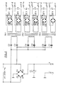
- the circuit shown in schematic number 1 is the control of the switching timing. This is supplied through output points labelled "A" and "B", these being components with equal magnitude in terms of switching time and frequency, but negated digitally between themselves.
- the duty cycle of the switching time is ruled by the input point denominated "G” and "C” with their voltage levels being compared by the integrated circuit denominated IC 1.
- the comonents marked with the following references: R-6, R-3, R-5, R4, C6, C3, D21, TR1 are a delay ist to regulate the start up and shut down sequence.
- the output point "E” corresponds to a 12 volt positive D.C. supply, with its general ground being in all the schematics, the point marked in schematic number 1 as "D".
- the circuit shown in schematic number 2 is the supply for the circuit shown in schematic number 5.
- This circuit includes a scheme for electronical isolation, which if desired, could be substituted by the circuit shown in schematic number 4 which is similar but does not include isolation between input and output.
- the supplies V3, V4, V5, and V6 are not used.
- the circuit shown in schematic number 3 is the general output of the groups of circuits or sub-assemblies.
- the components marked "C1,C2, and D1,D2,D3,D4, are the components that configure the basic cell for multiplying the input voltage, permiting the addition of however many cells are necessary to produce the desired voltage.
- the capacity of the capacitors of the basic cell will change depending on the current required by the load.
- the characteristics of the diodes in the basic cell will vary according to the current and voltage required for each application.
- the components marked TR1 and TR2 in schematic number 3 are two transformers with ferrous cores. The characteristics of these components will vary according to the current and voltage supplied by the voltage multiplication cells.
- the optocouples marked in schematic No. 3 and the I.C. marked I.C.1 as well as the components "R1,R2,R3,R4,R5,C7,D21” converts the current that circulates through R1 to a voltage on the point marked "G", this being proporcional to the intensity through R1.
- the points marked F-G-D in the schematic number 3 are sconnected to their corresponding letters in schematic number 1.
- the circuit shown in schematic number 4 illustrates the power amplifier for the entire circuit, ruled by the points marked A and B that come from the control circuit shown in schematic number 1.
- the integrated circuits marked IC3-IC4-IC5-IC6 are signal amplifiers used to attack the gates of the MOSFET transistors.
- the outputs marked I and J are connected to the inputs I and J respectivly in schematic number 3.
- the point marked H is the positive supply coming from the same point H in schematic number 2.
- the circuit shown in schematic number 5 shows, as does schematic number 4, the power amplifier for the entire circuit. the differance between the two circuits is that the circuit shown in schematic number 5 incorporates a scheme to isolate the input from the output by electronic switching, this being the fundamental mission of this circuit.
- the integrated circuits marked in the schematic as IC7-IC8- IC13-IC10-IC11-IC12-IC14 are signal amplifiers used to activate the gates of the MOSFET transistors.
- the outputs marked “I” and “J” are connected to the inputs marked “I” and “J” in the circuit of schematic number 3.
- the point marked “H” is a positive supply that comes from the same point on schematic number 3.
- the circuit shown in schematic number 6 shows a circuit to control the voltage level at the point marked "C". This control is done digitally and is compared by the circuit in schematic number 1.
- the point marked "C” in schematic 6 is connected to the same point in schematic number 1 the same being true for points "D” and "E” being connected to their respective points in schematic number 1.
- the I.C. marked IC3 does the function of digital to analogue converter, in the same way, the I.C's marked IC1-IC2 are 2 digital counters. The information in these counters is memorized by themselves due to the fact that their power source is maintained constant through a battery.
Landscapes
- Engineering & Computer Science (AREA)
- Power Engineering (AREA)
- Dc-Dc Converters (AREA)
- Rectifiers (AREA)
- Power Conversion In General (AREA)
- Inverter Devices (AREA)
Applications Claiming Priority (2)
| Application Number | Priority Date | Filing Date | Title |
|---|---|---|---|
| ES8702699A ES2008737A6 (es) | 1987-09-21 | 1987-09-21 | Circuito convertidor de alta eficacia para fuentes de alimentacion. |
| ES8702699 | 1987-09-21 |
Publications (2)
| Publication Number | Publication Date |
|---|---|
| EP0309375A2 true EP0309375A2 (fr) | 1989-03-29 |
| EP0309375A3 EP0309375A3 (fr) | 1990-01-17 |
Family
ID=8252559
Family Applications (1)
| Application Number | Title | Priority Date | Filing Date |
|---|---|---|---|
| EP88500085A Withdrawn EP0309375A3 (fr) | 1987-09-21 | 1988-09-21 | Circuit de conversion à haut rendement pour alimentation de puissance |
Country Status (4)
| Country | Link |
|---|---|
| US (1) | US5023767A (fr) |
| EP (1) | EP0309375A3 (fr) |
| JP (1) | JPH01194860A (fr) |
| ES (1) | ES2008737A6 (fr) |
Families Citing this family (2)
| Publication number | Priority date | Publication date | Assignee | Title |
|---|---|---|---|---|
| US8369116B2 (en) * | 2010-03-01 | 2013-02-05 | Raymond Peter Maroon | Isolated DC-to-DC power converter topology |
| US8816654B2 (en) | 2010-09-27 | 2014-08-26 | Cooper Technologies Company | Universal-voltage discrete input circuit |
Family Cites Families (5)
| Publication number | Priority date | Publication date | Assignee | Title |
|---|---|---|---|---|
| US3465231A (en) * | 1967-12-26 | 1969-09-02 | Varo | Transformerless converter-inverter |
| US3579078A (en) * | 1969-10-06 | 1971-05-18 | Trw Inc | Constant current high-voltage power supply |
| US4298926A (en) * | 1979-06-29 | 1981-11-03 | The United States Of America As Represented By The Administrator Of The National Aeronautics And Space Administration | Power converter |
| US4399499A (en) * | 1981-12-18 | 1983-08-16 | Gte Automatic Electric Labs Inc. | Bi-lateral four quadrant power converter |
| DE3472867D1 (en) * | 1984-02-29 | 1988-08-25 | Ibm | Power switching circuit |
-
1987
- 1987-09-21 ES ES8702699A patent/ES2008737A6/es not_active Expired
-
1988
- 1988-09-20 JP JP63236187A patent/JPH01194860A/ja active Pending
- 1988-09-21 EP EP88500085A patent/EP0309375A3/fr not_active Withdrawn
-
1990
- 1990-04-09 US US07/506,575 patent/US5023767A/en not_active Expired - Fee Related
Also Published As
| Publication number | Publication date |
|---|---|
| ES2008737A6 (es) | 1989-08-01 |
| US5023767A (en) | 1991-06-11 |
| JPH01194860A (ja) | 1989-08-04 |
| EP0309375A3 (fr) | 1990-01-17 |
Similar Documents
| Publication | Publication Date | Title |
|---|---|---|
| US5179508A (en) | Standby boost converter | |
| EP0500789B1 (fr) | Systeme d'alimentation ininterrompue a circuit ameliore de correction du facteur de puissance | |
| US5583753A (en) | Parallel control type DC--DC converter | |
| RU2222084C2 (ru) | Устройство управления параллельной работой преобразователей постоянного напряжения, прежде всего в имеющей несколько уровней напряжения электрической бортовой сети транспортного средства | |
| US5461264A (en) | Multi-voltage control circuit of battery or multiple independent DC power | |
| US5680300A (en) | Regulated charge pump DC/DC converter | |
| US5939871A (en) | DC/DC converter and controller therefor utilizing an output inductor current and input voltage | |
| US5164890A (en) | Current share scheme for parallel operation of power conditioners | |
| US5489837A (en) | AC-DC converter having improved power factor to control feedback signal corresponding to output voltage of constant control circuit | |
| US4521725A (en) | Series switching regulator | |
| KR20010014757A (ko) | 단일 인덕터를 갖는 다중 출력 벅 변환기 | |
| US4581690A (en) | Switched-mode power supply with output post-regulator | |
| KR19990007348A (ko) | 디씨-디씨 전력 변환기를 위한 다이내믹 조정기 및 관련 방법 | |
| US6239585B1 (en) | Self-oscillating switch-mode DC to DC conversion with current switching threshold hysteresis | |
| US5045768A (en) | Off-line battery charger | |
| US4353114A (en) | DC/DC Converter | |
| EP0309375A2 (fr) | Circuit de conversion à haut rendement pour alimentation de puissance | |
| JPH03169255A (ja) | 昇圧型dc―dcコンバータ | |
| US5982644A (en) | Voltage boost circuit for a high voltage converter | |
| JPH06141536A (ja) | Dc/dcコンバータを含む低損失電源供給装置 | |
| US7230351B2 (en) | Circuit arrangement for stabilizing a supply voltage and method for operating said circuit arrangement | |
| JP2025116691A (ja) | 整流回路、整流回路の制御方法、及び電力システム | |
| JP2003180073A (ja) | 電源回路 | |
| US7309968B2 (en) | Motor control circuit and associated full bridge switching arrangement | |
| US5612611A (en) | Switching regulator with dyssymetrical differential input stage |
Legal Events
| Date | Code | Title | Description |
|---|---|---|---|
| PUAI | Public reference made under article 153(3) epc to a published international application that has entered the european phase |
Free format text: ORIGINAL CODE: 0009012 |
|
| AK | Designated contracting states |
Kind code of ref document: A2 Designated state(s): DE FR GB IT NL SE |
|
| PUAL | Search report despatched |
Free format text: ORIGINAL CODE: 0009013 |
|
| AK | Designated contracting states |
Kind code of ref document: A3 Designated state(s): DE FR GB IT NL SE |
|
| RHK1 | Main classification (correction) |
Ipc: H02M 3/10 |
|
| 17P | Request for examination filed |
Effective date: 19900713 |
|
| 17Q | First examination report despatched |
Effective date: 19920720 |
|
| STAA | Information on the status of an ep patent application or granted ep patent |
Free format text: STATUS: THE APPLICATION HAS BEEN WITHDRAWN |
|
| 18W | Application withdrawn |
Withdrawal date: 19921110 |
|
| R18W | Application withdrawn (corrected) |
Effective date: 19921110 |